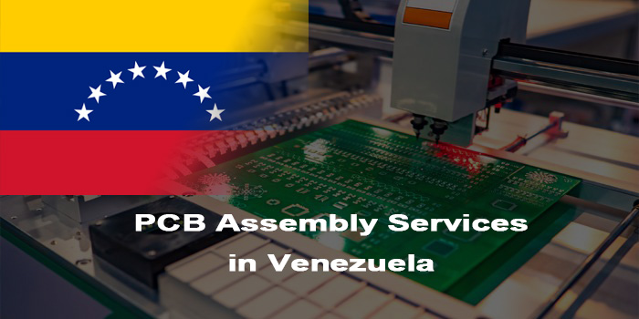
Tired of searching for high-quality PCB assembly services in Venezuela you can truly trust? EBest delivers professional PCB assembly in Venezuela with consistent quality, fast turnaround, and full certifications for medical, aerospace, industrial, and mission‑critical projects.
Why EBest Is Your Most Trusted PCB Assembly Services in Venezuela?
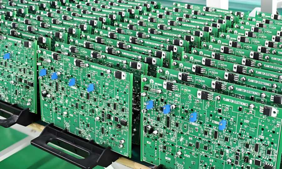
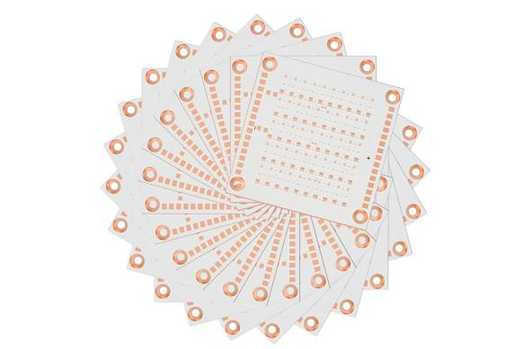
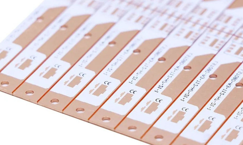
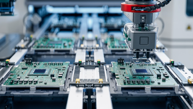
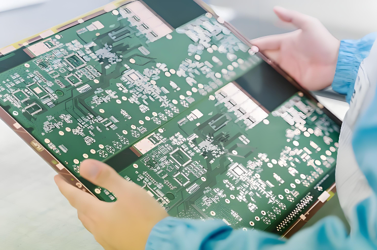
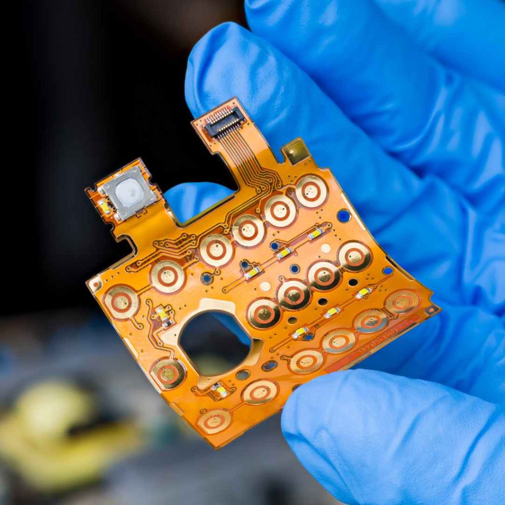
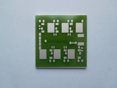
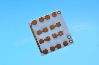
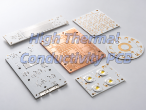
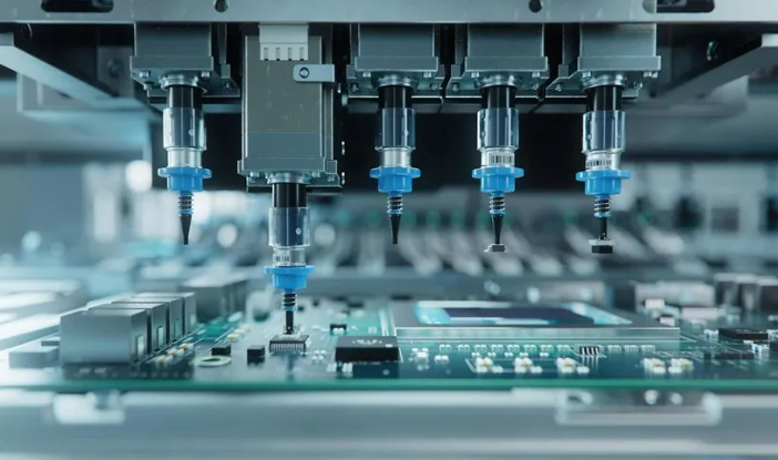
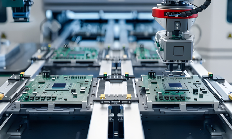
When you source PCB assembly services in Venezuela, you need a partner that delivers consistency, not excuses. EBest has mastered PCB assembly in Venezuela by combining automated production, strict quality systems, and end-to-end support. Unlike many PCB assembly companies in Venezuela, we own full certifications, operate high-precision lines, and maintain a 98.7% on-time delivery rate. Each month, we produce 1,000+ unique PCB designs across medical, aerospace, industrial, and automotive fields. From early prototypes to high-volume mass production, our PCB assembly in Venezuela is engineered to eliminate risk and accelerate your success.
Common Pain Points in PCB Assembly in Venezuela & How We Solve Them
Businesses across Venezuela often face frustrating challenges: long and unpredictable lead times, unreliable component availability, weak fine‑pitch soldering, insufficient testing, missing industry certifications, and slow technical support. These issues create project delays, extra rework, and unnecessary risk.
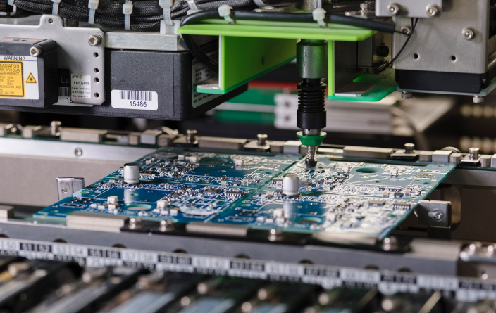
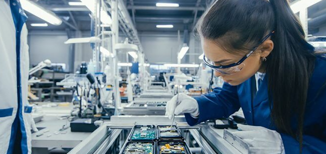
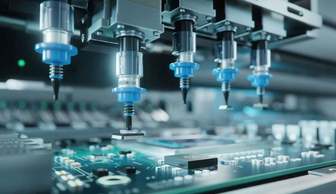
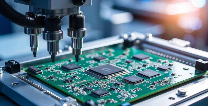
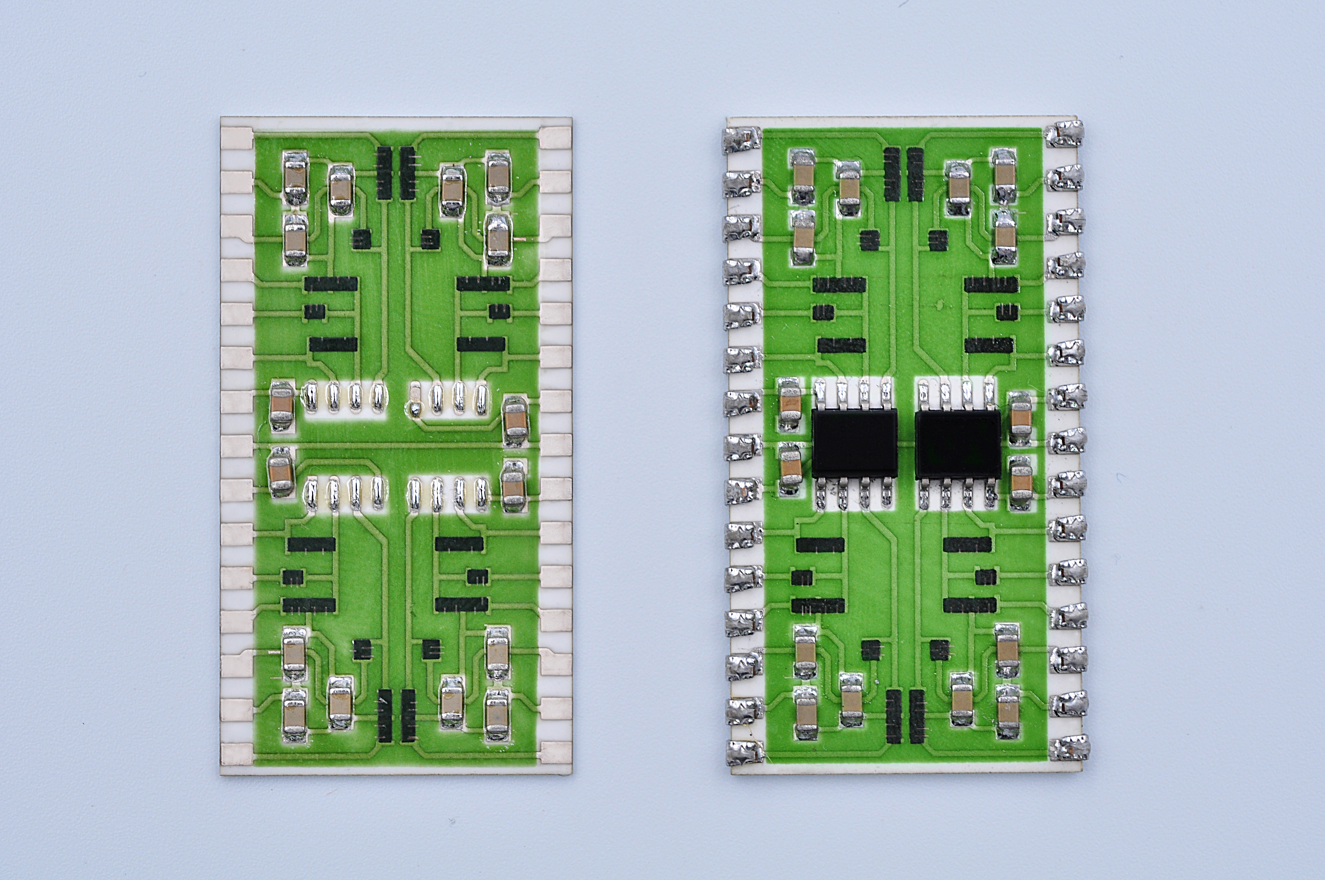
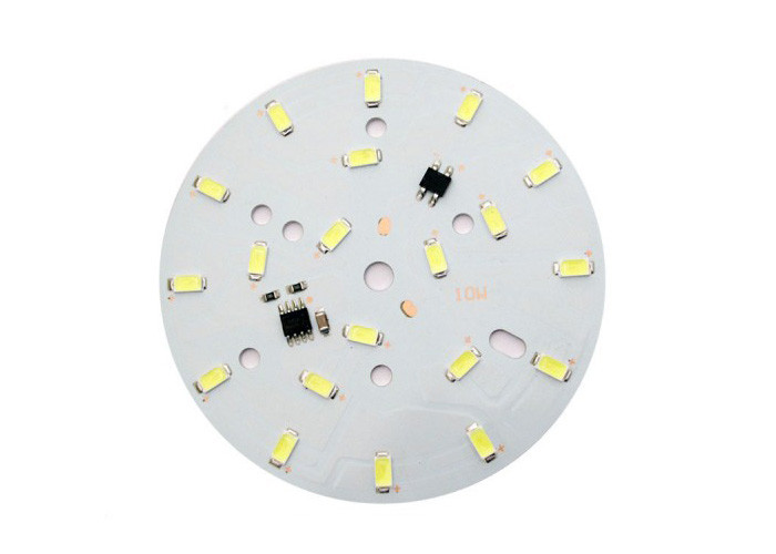
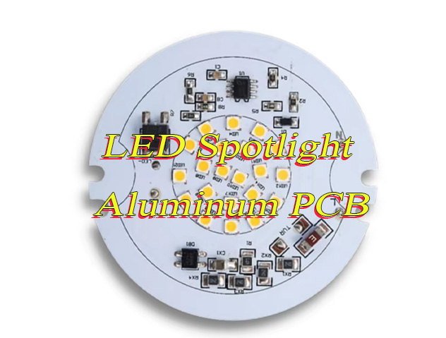
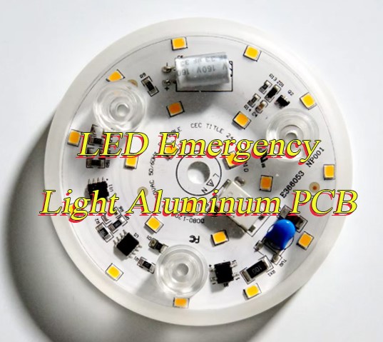
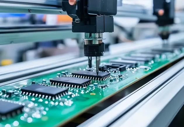
We deliver fast, predictable turnaround for PCB assembly in Venezuela to keep your projects on track. Our global component network supports consistent sourcing for SMD, BGA, QFN, QFP and specialized parts, keeping production steady. Our advanced assembly lines handle ultra‑small components down to 01005 and fine‑pitch BGA down to 0.25mm with exceptional precision. We perform full inspection on every order to catch and eliminate defects before shipping.
We hold complete industry certifications for medical, aerospace, automotive, and industrial applications, including IATF 16949, ISO 9001, ISO 13485, AS9100D. Our engineering team provides responsive, clear support for every stage of your PCB assembly in Venezuela. When you choose EBest, you avoid the risks and frustrations of unreliable PCB assembly manufacturer in Venezuela partners.
Why Choose EBest for PCB Assembly Companies in Venezuela?
EBest does more than assemble boards, we help you reduce risk, speed up launches, cut rework, and win more high‑value projects across Venezuela.
- Over 19 years of focused PCB experience means fewer errors, smoother production, and better long-term reliability for your PCB assembly in Venezuela.
- Monthly production capacity of 260,000 square feet supports any order size, from small prototypes to large mass production, so you never outgrow your partner.
- Component placement speed up to 13,200,000 chips per day shortens your lead times and gets your products to market faster.
- Precision capabilities down to 01005 components and 0.25mm BGA pitch let you build smaller, smarter, more advanced products that stand out in the market.
- In-house PCB fabrication, component sourcing, assembly, and testing create a single-point solution that saves you time, cuts coordination hassle, and improves consistency.
- 24‑hour expedite service ensures your urgent projects move forward without delay, keeping you ahead of competitors.
- Full certifications including IATF 16949, ISO 13485, AS9100D let you bid and win medical, aerospace, and automotive projects locally and globally.
- 100% full inspection on every order drastically reduces failures, returns, and rework, lowering your total cost per board.
- Free DFM & engineering support keeps your project on track, with clear updates and fast solutions to keep production moving and reduce reworking cost a lot.
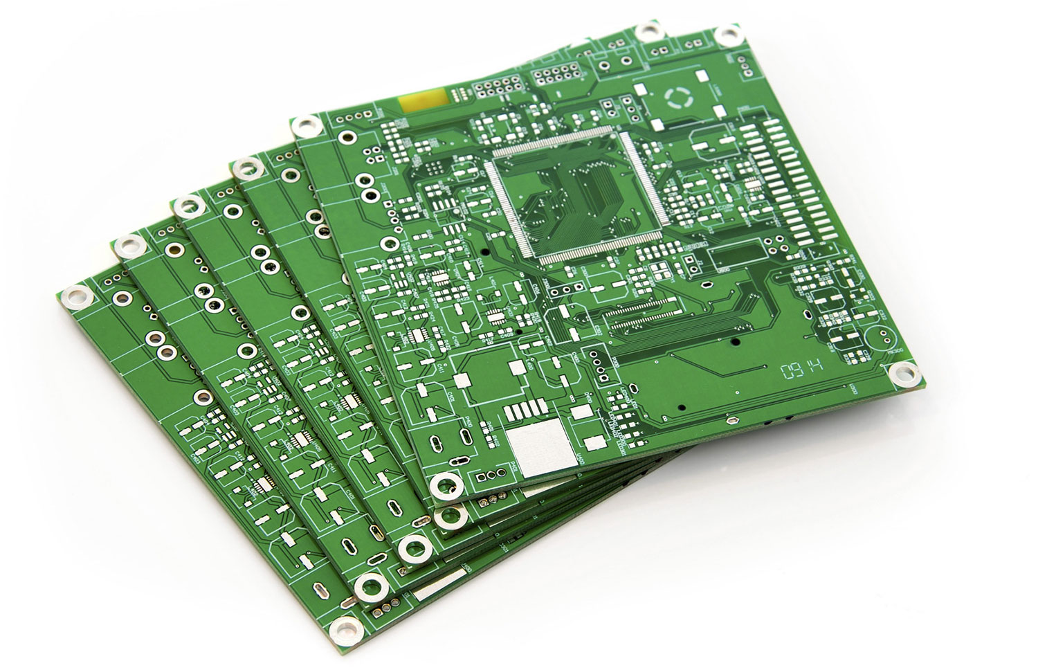
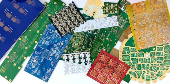
Full PCB Assembly Services in Venezuela Provided By EBest
Below are PCB assembly services in Venezuela we offer you:
- SMT Assembly – High‑precision surface mount assembly for modern electronics.
- Through‑Hole (THT) Assembly – Durable, reliable through‑hole component soldering.
- Mixed SMT + THT Assembly – Flexible assembly for mixed‑technology designs.
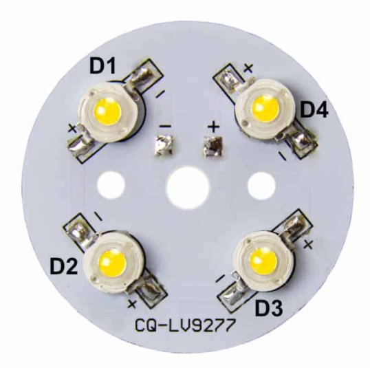
- BGA Assembly Service – Fine‑pitch BGA, QFN, and QFP with full verification.
- Prototype PCB Assembly – Fast, reliable prototypes for product development.
- Quick Turn PCB Assembly – Rush services for time‑sensitive projects.
- Full Turnkey PCB Assembly – All‑in‑one solution from design to finished product.
- Box Assembly – Complete box build, integration, and final functional testing.
What Quality Certifications Does EBest Hold for Venezuela PCBA Orders?
EBest maintains a complete set of internationally recognized certifications to ensure every PCB assembly in Venezuela meets the strictest global requirements. Each certification is regularly audited and updated to maintain full compliance.
- IATF 16949: Automotive quality management system for high‑reliability automotive electronics. Ensures full traceability, zero-defect targets, and strict process control for vehicle safety components.
- ISO 9001:2015: Global general quality management standard. Demonstrates consistent process control, customer focus, and continuous improvement in all PCB assembly services in Venezuela.
- ISO 13485:2016: Medical device quality system for life‑critical medical electronics. Supports full traceability, risk management, and strict controls for diagnostic, monitoring, and therapeutic equipment.
- AS9100D: Aerospace and defense quality standard. Designed for high‑reliability performance in extreme environments, including aircraft systems, navigation, and communication equipment.
- RoHS Compliance: Restriction of hazardous substances. All assemblies are free of lead, mercury, cadmium, and other dangerous materials for global market access.
- REACH Compliance: European environmental regulation for chemical safety. Ensures full material transparency and safe use of components in PCB assembly in Venezuela.
- UL Certification: Global safety certification for electronic products. Ensures electrical safety, flammability resistance, and long‑term reliability for commercial and industrial use.
Every PCB assembly in Venezuela produced by EBest follows certified processes, full material traceability, and strict quality controls.
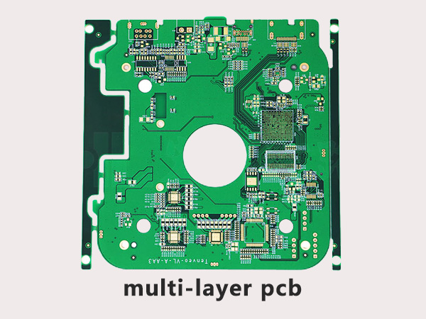
Advanced PCB Assembly Capabilities We Offer in Venezuela
| Item | Capabilities |
| Placer Speed | 13,200,000 chips/day |
| Bare Board Size | 0.2 x 0.2 inches – 20 x 20 inches/ 22*47.5 inches |
| Minimum SMD Component | 01005 |
| Minimum BGA Pitch | 0.25mm |
| Maximum Components | 50*150mm |
| Assembly Type | SMT, THT, Mixed assembly |
| Component Package | Reels, Cut Tape, Tube, Tray, Loose Parts |
| Lead Time | 1 – 5 days |
How We Ensure On‑Time PCB Assembly Delivery in Venezuela?
On‑time delivery is essential for PCB assembly services in Venezuela and critical to your product launches and production plans. We maintain highly streamlined workflows to meet your deadlines reliably:
- Standard orders: 3 to 5 business days.
- Prototype and quick‑turn orders: 1 to 2 business days.
- Urgent orders: 24‑hour expedite shipping for critical projects.
Our stable production flow, automated equipment, in‑house fabrication, and reliable component supply chain help us deliver on time, every time. We provide transparent order tracking and regular updates so you always know the status of your PCB assembly in Venezuela. With EBest, you never miss critical product launches, production deadlines, or customer commitments.
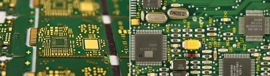
Strict Quality Control for High‑Reliability PCB Assembly in Venezuela
Quality is built into every step of our PCB assembly in Venezuela with a full‑cycle quality management system:
- Full incoming material inspection for components, bare PCBs, and auxiliary materials to ensure authenticity and quality.
- Precise solder paste control and SPI (Solder Paste Inspection) for strong, consistent solder joints.
- High‑accuracy component placement with tight tolerances for micro and fine‑pitch parts.
- Automated optical inspection (AOI) to detect visible assembly defects such as misalignment, missing parts, or poor soldering.
- X‑ray inspection for hidden BGA, QFN, and leadless package solder joints that cannot be seen visually.
- Functional electrical testing to confirm performance meets your exact specifications.
- Final full inspection before packaging and shipment to ensure zero defects.
- ESD‑safe production environment to protect sensitive electronic components.
- Full material and production traceability for compliance and quality tracking.
- Strict adherence to IPC‑A‑610 international electronics assembly standards.
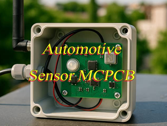
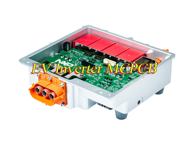
Industry Applications: Medical, Aerospace & Industrial PCB Assembly
Medical Device PCB Assembly
We provide certified PCB assembly for patient monitors, diagnostic tools, portable medical devices, surgical equipment, and therapeutic machines. Our strict processes, full traceability, and ISO 13485 certification meet strict medical safety and reliability requirements. We deliver zero‑defect, long‑life boards that support life‑critical operations and regulatory compliance. Our PCB assembly in Venezuela ensures consistent quality for sensitive health‑care applications.
Aerospace & Defense PCB Assembly
Approved PCB assembly for flight systems, sensors, navigation equipment, communication units, and defense electronics. Boards are built to perform reliably in extreme temperatures, high vibration, shock, and harsh environmental conditions. Our AS9100D certification and strict quality controls meet the most demanding aerospace reliability standards. Our PCB assembly services in Venezuela support mission‑critical aerospace and defense projects.
Industrial Equipment PCB Assembly
Qualified PCB assembly for automation controllers, power supplies, drive systems, sensors, and factory automation equipment. Built to operate continuously 24/7 in tough industrial conditions including dust, heat, and electrical interference. Our IATF 16949 and ISO 9001 processes ensure stability, durability, and long service life. We deliver stable, long‑lasting PCB assembly in Venezuela for heavy‑duty industrial use.
Custom PCB Assembly Solutions for Your Venezuelan Projects
Off‑the‑shelf services often cannot meet unique engineering requirements. We provide fully custom PCB assembly services in Venezuela tailored to your product needs:
- Custom substrate materials and layer configurations for specific electrical or thermal performance.
- Special surface finishes and protective coatings to extend product life in harsh environments.
- Professional DFM (Design for Manufacturability) review to optimize your design for higher yield and lower cost.
- Custom functional testing protocols for strict performance and safety requirements.
- Flexible order sizes from prototypes to full mass production to support your development cycle.
- Personalized project management and engineering support for complex projects.
Our engineering team works closely with you to create the ideal PCB assembly in Venezuela for your product.
Prototype & Low-Volume PCB Assembly in Venezuela
Prototype and low‑volume PCB assembly in Venezuela from EBest helps you validate designs quickly, reduce project risk, and speed up time‑to‑market without unnecessary costs. We support small‑batch runs that let you test form, fit, and function before mass production, keeping your development cycle efficient and flexible.
Our prototype PCB assembly in Venezuela uses the same strict production and inspection standards as high‑volume manufacturing, so your test results are fully reliable and consistent with future mass production. Every small‑batch order receives complete quality checks to ensure stable performance during testing and validation.
We offer fast turnaround for prototypes and low‑volume orders, along with free DFM reviews to optimize your design for better yield and lower production costs later. With EBest, you get responsive, high‑quality PCB assembly in Venezuela that supports innovation, shortens development time, and strengthens your final product.
FAQ About PCB Assembly Services in Venezuela
Q1: What is the minimum order quantity for PCB assembly in Venezuela?
A1: We accept 1-5 piece prototypes, low‑volume, and mass‑production orders with no strict minimums to support your business needs.
Q2: Can you handle small components and fine‑pitch BGA?
A2: Yes, we regularly assemble ultra‑small components down to 01005 and fine‑pitch BGA down to 0.25mm with full inspection.
Q3: Do you hold certifications for medical, aerospace and automotive?
A3: Yes, we hold IATF 16949 (automotive), ISO 13485 (medical), and AS9100D (aerospace) certifications.
Q4: How fast can you deliver PCB assembly in Venezuela?
A4: We offer standard (3–5 days), quick‑turn (1–2 days), and 24‑hour expedite services for urgent needs.
Q5: Do you provide full turnkey PCB assembly in Venezuela?
A5: Yes, we offer complete turnkey service including fabrication, components, assembly, testing, and box build.
Q6: Can you assemble flex, rigid‑flex and ceramic PCBs?
A6: Yes, we provide expert assembly for flex, rigid‑flex, ceramic, and high‑frequency PCBs.
Q7: Do you inspect every board before shipment?
A7: Yes, full inspection including AOI and X‑ray is standard on every order to ensure zero defects.
Q8: How can I request a quote?
A8: Send your Gerber files and BOM to sales@bestpcbs.com for a fast, free, no‑obligation quote.