





Wire bonding EPIG thickness is not governed by one universal IPC value. Published EPIG studies and supplier guidance commonly evaluate or use palladium from about 0.05 to 1.0 µm and immersion gold from about 0.05 to 0.20 µm, while a narrower starting window around 0.10–0.15 µm Pd and 0.10–0.20 µm Au appears in practical process guidance. These numbers are starting points, not automatic acceptance limits.
The approved thickness must match the wire material, bond method, pad geometry, cleaning process, thermal history, and reliability target. It must also be confirmed by coating measurement and wire-bond testing. This guide separates nickel-free EPIG from ENEPIG and shows how engineers can turn a published range into a controlled fabrication requirement.
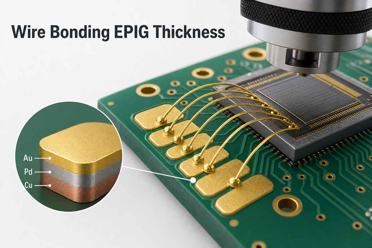
What Are the Wire Bonding EPIG Thickness Requirements?
The essential requirement is a project-specific Pd/Au thickness window backed by the fabricator’s chemistry limits and the assembler’s bond qualification. EPIG does not have a universal IPC finish specification equivalent to the ENEPIG specification in IPC-4556. A drawing that says only “EPIG per IPC-4556” mixes two different finishes and leaves the actual EPIG deposit uncontrolled.
A useful starting specification should identify:
- Finish stack: electroless palladium over copper, followed by immersion gold, with no electroless nickel layer.
- Pd and Au thickness: separate nominal values or minimum/maximum limits for each layer.
- Bond process: wire material, wire diameter, ball or wedge bonding, and expected process window.
- Thermal exposure: assembly reflow, bake, storage, and any aging condition before bonding.
- Acceptance method: XRF measurement plan, wire-pull criteria, failure-mode review, and sampling level.
Do not convert an experimental window into a production guarantee without qualification. The useful question is not “What is the thickest coating?” but “Which controlled deposit produces stable bonds after the real assembly history?”
Wire Bonding EPIG Thickness Chart
The following chart separates published evidence from a production specification. It gives engineering starting points without presenting them as universal limits.
| Layer or Control | Published or Practical Starting Range | What Must Be Confirmed |
| Electroless palladium | 0.05–1.0 µm in a published DoE; about 0.10–0.15 µm in practical process guidance | Coverage, diffusion barrier performance, solder interaction, and process capability |
| Immersion gold | 0.05–0.20 µm in published studies; about 0.10–0.20 µm as a practical starting window | Bondability, surface condition, porosity, thermal aging, and pull-test result |
| Gold wire | 1.0 mil wire was used in one published EPIG study | Actual wire alloy, diameter, ball geometry, and bonding parameters |
| Qualification | No single universal EPIG acceptance window | XRF mapping, wire pull, failure location, aging, and lot controls |
Thickness units must be unambiguous. One micrometre equals about 39.37 microinches. Keep the drawing in one unit system or show both units with a controlled conversion; do not let a supplier infer whether a value means µm or µin.
What Is EPIG, and How Is It Different from ENEPIG?
EPIG is a nickel-free finish with copper, electroless palladium, and immersion gold. ENEPIG adds electroless nickel between copper and palladium. That one layer changes the diffusion path, deposit structure, process control, and the standards that can be cited.
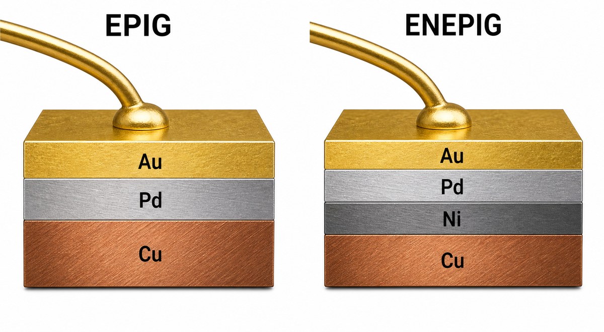
| Finish | Layer Stack | Specification Point |
| EPIG | Cu / Pd / Au | No universal IPC finish thickness specification; define and qualify the project window |
| ENEPIG | Cu / Ni / Pd / Au | IPC-4556 addresses ENEPIG, not nickel-free EPIG |
| ENIG | Cu / Ni / Au | Different surface chemistry and wire-bond behavior; do not reuse EPIG limits |
This distinction matters because many search results for “wire bonding EPIG thickness” actually provide ENEPIG values. For background on the nickel-containing finish, see our ENEPIG PCB finish guide and our comparison of ENIG vs ENEPIG.
Why Does Gold Thickness Affect Wire-Bond Performance?
Gold thickness affects the condition of the top surface that receives the bond. In a published EPIG design of experiments using 1.0 mil gold wire, increasing the immersion-gold thickness improved the wire-pull response more clearly than changing palladium thickness. That finding supports tighter control of the Au deposit, but it does not establish one best value for every bonding process.
Gold that is too thin for the chosen chemistry and thermal history can leave a surface more sensitive to palladium exposure, porosity, contamination, or diffusion effects. Simply specifying “more gold” is not a complete solution either. The immersion process has its own chemistry window, and the bond must be evaluated after the same storage, bake, plasma clean, and assembly exposure expected in production.
What Does Palladium Thickness Control?
Palladium separates the immersion-gold surface from copper and can act as a diffusion barrier. In one aging study, a 0.15 µm Pd deposit reduced copper diffusion under the tested 175°C for 16-hour condition. The same result should not be treated as a universal minimum because the result depends on deposit quality, chemistry, temperature, time, and the rest of the assembly process.
In the published EPIG DoE, palladium thickness had a stronger practical effect on solder-joint shear than on gold-wire pull. That is important for pads expected to support both soldering and wire bonding: the specification should protect both interfaces rather than optimize one result in isolation.
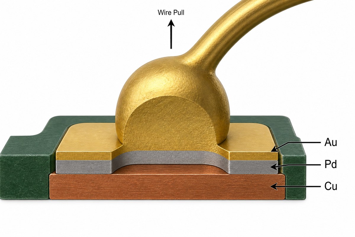
How Do Wire Type and Bonding Method Change the Required Thickness?
Wire bonding thickness cannot be selected independently of the bonding system. Gold ball bonding, gold wedge bonding, aluminum wire, copper wire, and ribbon bonding apply different ultrasonic energy, force, temperature, and deformation to the pad.
- Wire material and diameter: change bond deformation and required interfacial strength.
- Ball or wedge process: changes contact geometry and the way force and ultrasonic energy enter the pad.
- Pad size and support: affect stress concentration, bond placement tolerance, and pad-lift risk.
- Bonding parameters: force, ultrasonic power, time, and temperature must be developed together.
- Surface preparation: contamination, oxidation, handling, and plasma cleaning can change the result even when XRF thickness is correct.
Define the wire process before freezing the finish. Our guides to gold wire bonding and wire-bonding pad design cover two other parts of the same interface.
What Should the Fabrication Drawing Specify?
The drawing should state the exact EPIG stack, separate Pd and Au limits, and the approved measurement and qualification requirements. Avoid a generic finish note that forces the fabricator to guess.
A controlled callout can include:
- Finish: “Nickel-free EPIG: electroless Pd / immersion Au over Cu.”
- Thickness: project-approved Pd and Au minimum/maximum limits in µm or µin.
- Applicable pads: whether EPIG applies to all exposed copper or only selected wire-bond pads.
- Measurement: XRF method, coupon or pad locations, sample quantity, and reporting requirement.
- Bonding use: wire material, diameter, bond type, and thermal exposure before bonding.
- Acceptance: approved wire-pull method, minimum force or statistical limit, and acceptable failure modes.
Do not cite IPC-4556 as though it were an EPIG finish specification. If ENEPIG is acceptable as an alternative, list it separately and require written approval before substitution.
How Should EPIG Thickness Be Measured?
X-ray fluorescence is the normal non-destructive method for measuring thin metallic deposits, but the measurement plan matters as much as the instrument. The XRF method must be calibrated for the Cu/Pd/Au stack, and the aperture must suit the pad or coupon size.
A practical plan should cover:
- multiple locations across the production panel, not one convenient coupon reading;
- separate reporting of Pd and Au thickness;
- defined edge exclusion where pad geometry can distort the reading;
- measurement-system checks using traceable reference standards;
- lot records that connect the coating results to the bond-test samples.
XRF confirms deposit thickness. It does not by itself prove cleanliness, bondability, adhesion, or reliability after thermal aging.
Which Tests Qualify EPIG for Wire Bonding?
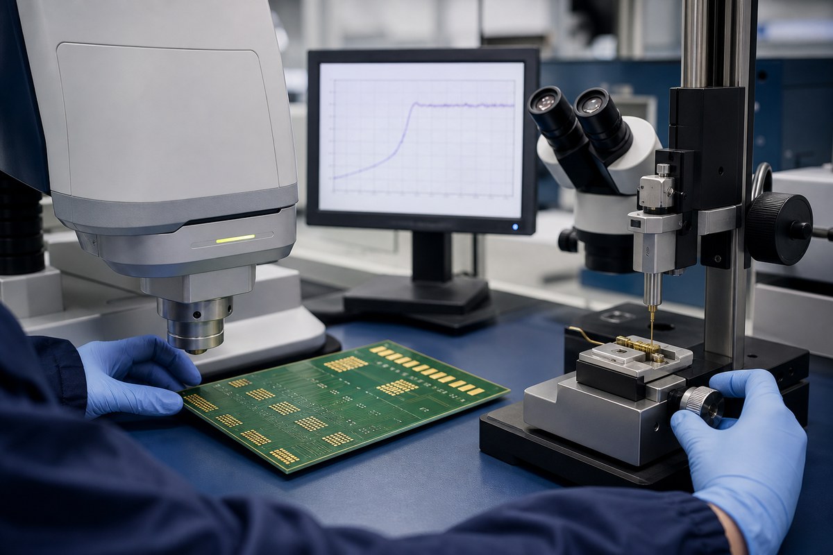
A useful qualification combines coating data with wire-pull results and failure-mode inspection. One published EPIG study used MIL-STD-883 Method 2011, Condition D for wire pull, but the project team must select the method, sample size, and acceptance criteria that match its package and reliability class.
- As-plated bond test: establishes the initial process window.
- Post-clean test: verifies that plasma or chemical preparation does not damage the finish.
- Thermal-aging test: exposes diffusion or surface degradation that an immediate test can miss.
- Wire-pull distribution: evaluates variation, not only the average.
- Failure-mode analysis: distinguishes wire break, heel break, interfacial lift, and pad or metallization failure.
- Solder test where applicable: confirms pads serving both solder and wire-bond functions.
Record the bonding parameters with the result. A passing pull number without force, ultrasonic power, time, temperature, capillary, and wire-lot data is difficult to reproduce.
What Causes EPIG Wire-Bond Failures?
EPIG wire-bond failures usually come from the interaction of surface condition, deposit control, bonding parameters, pad construction, and thermal history rather than thickness alone.
- Surface contamination: handling residue, organic films, or poor rinsing can block metal-to-metal contact.
- Thin or non-uniform Au: can increase sensitivity to exposed Pd, porosity, and local variation.
- Diffusion after heat exposure: can change the top-surface chemistry before bonding.
- Uncontrolled Pd deposit: may compromise barrier behavior or the combined solder/bond requirement.
- Incorrect bonding recipe: insufficient energy causes weak interfaces; excessive energy or force can damage the pad or heel.
- Poor pad design: small pads, weak copper anchoring, or nearby mask geometry can reduce the process margin.
When a bond fails, compare the actual break location with XRF maps, surface analysis, process logs, and thermal history. Raising ultrasonic energy without identifying the interface can hide the cause and create a new failure mode.
When Should You Choose EPIG Instead of ENEPIG?
Choose EPIG when the design has a justified need for a nickel-free bond-pad finish and the supply chain can qualify that exact Cu/Pd/Au process. Consider ENEPIG when the established nickel barrier, IPC-4556 framework, and broader fabrication availability better fit the product.
| Decision Factor | EPIG | ENEPIG |
| Metal stack | Nickel-free Cu / Pd / Au | Cu / Ni / Pd / Au |
| Specification route | Supplier- and project-qualified window | IPC-4556 plus project requirements |
| Engineering burden | More explicit process confirmation and validation | More standardized industry framework |
| Best fit | Products that specifically need a nickel-free finish | Mixed soldering and wire-bond applications that accept nickel |
Do not select EPIG only because a search result gives a thinner stack. Availability, minimum order, qualification work, yield, test cost, and lead time can outweigh the material difference. Confirm the finish with both the PCB fabricator and the wire-bond assembly team before design release.
FAQ About Wire Bonding EPIG Thickness
Is IPC-4556 an EPIG thickness standard?
No. IPC-4556 covers ENEPIG, which contains an electroless nickel layer. Nickel-free EPIG needs a separate supplier-supported and project-qualified thickness callout.
Can one wire bonding thickness work for every wire material?
No. Wire alloy, diameter, ball or wedge process, bonding parameters, pad geometry, and thermal history change the required process window.
Does thicker gold always produce a stronger bond?
No. Published EPIG work shows that Au thickness can materially affect wire pull, but deposit chemistry, surface condition, aging, and bonding parameters still control the final result. Use a qualified window rather than an unlimited “thicker is better” rule.
Can wire bonding ENEPIG data be used for EPIG?
Not directly. Wire bonding ENEPIG data includes the effect of a nickel layer that EPIG does not have. It can inform a comparison, but it cannot replace EPIG-specific testing.
Should EPIG be tested after thermal aging?
Yes, when the product will see bake, reflow, storage, or other heat exposure before or after bonding. Aging can reveal diffusion and surface changes that an as-plated test misses.
How Can EBest Circuit Review Your Wire-Bonding PCB Build?
At EBest Circuit, we support PCB and PCBA projects that include wire-bonding requirements. For a nickel-free EPIG request, we will first review the finish callout and confirm process availability rather than assume that ENEPIG data applies.
Send your Gerber files, fabrication drawing, pad map, wire material and diameter, bond method, thermal history, test criteria, quantity, and required delivery date to sales@bestpcbs.com. We can then review the build, identify missing controls, and discuss a practical qualification path. Revisit this wire bonding EPIG thickness guide when preparing the finish and acceptance notes.







