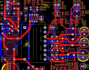
USB motherboard pinout errors can damage a port, prevent device enumeration, or force a board respin. Common causes include a reversed connector view, incorrect footprint, swapped differential pair, missing protection, or an uncontrolled assembly drawing.
This guide compares common internal USB headers and the checks needed before PCB fabrication and assembly. Always follow the released motherboard manual, connector drawing, USB specification, and customer-approved electrical design.
What a USB Motherboard Pinout Shows
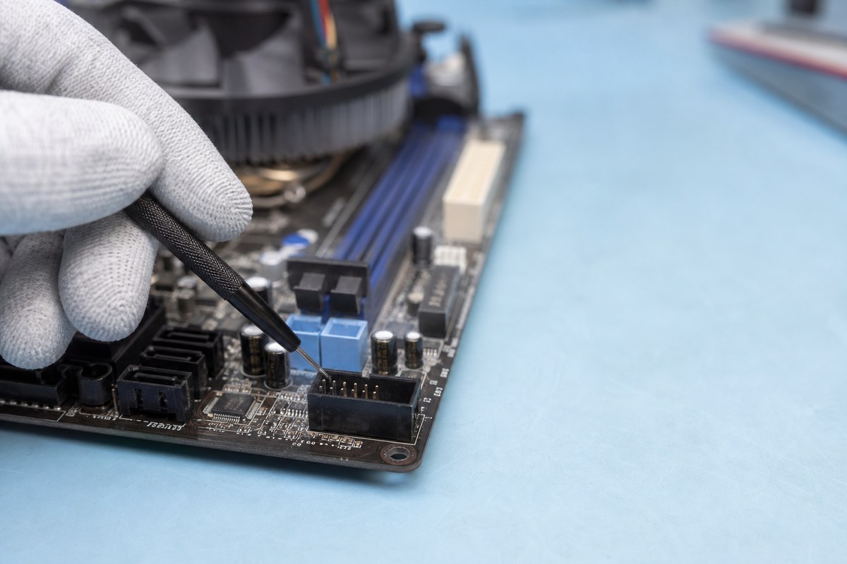
A USB motherboard pinout maps each header position to power, ground, USB 2.0 data, SuperSpeed pairs, sideband, shield, key, or no-connect functions.
Confirm the drawing view before comparing signals. Pin 1, row numbering, key position, and latch direction must agree across the schematic, footprint, assembly drawing, cable drawing, and inspection record.
Before approving a pinout, confirm four things:
- The exact connector part number and its manufacturer drawing.
- The viewing direction used by every pin-number diagram.
- The signal-to-pin mapping in the released schematic and netlist.
- The mating cable or front-panel assembly, including any proprietary wiring.
Matching pin counts do not prove matching assignments. OEM and custom boards may use proprietary keying or pin maps.
USB Motherboard Connector Types
USB generation and mechanical header type are separate decisions. USB 2.0, USB 3.x, and front-panel Type-C headers use different connectors and signal sets.
| Header type | Typical form | Main signals | Buyer check |
| USB 2.0 internal header | 2 x 5 positions, commonly one key/missing pin | Two USB 2.0 ports: power, D-, D+, ground | Confirm key position and whether pin 10 is NC, shield, or overcurrent-related. |
| USB 3.x front-panel header | Shrouded 19/20-position family | USB 2.0 lines plus SuperSpeed TX/RX pairs, power, ground | Confirm connector revision, pair polarity, pair naming, and mating cable. |
| Front-panel USB Type-C header | Compact Type-E/Key-A style family | High-speed lanes and control/sideband functions depend on implementation | Confirm the exact standard revision, connector drawing, orientation, and controller architecture. |
An adapter may solve a mechanical mismatch, but it does not confirm bandwidth, power, controller support, or pin assignment.
USB 2.0 Header Pinout and Keying
A common USB 2.0 header serves two ports, each using +5 V, D-, D+, and ground. A missing pin or blocked cavity provides keying; the remaining position may be NC, shield, or overcurrent-related.
An incorrect USB 2.0 connection can cause several different outcomes:
- VBUS applied to a data or ground position can damage the port or connected device.
- D+ and D- swapped within a port can prevent enumeration or create intermittent behavior.
- A connector installed in the wrong orientation can defeat the intended protection of the missing key pin.
For a new PCB, verify pin 1, key location, footprint orientation, courtyard, housing clearance, solder mask, and assembly notes. For an existing board, use its exact manual and revision.
USB 3.0 Header Signals and Pair Routing
A USB 3.0 front-panel header combines USB 2.0 signals with SuperSpeed TX/RX pairs, power, ground, and shield or drain connections. More signals make routing and documentation errors more costly.
TX/RX labels can appear reversed when drawings describe opposite sides of the interface. Confirm the naming convention and connector view before changing net names.
PCB review should cover:
- Differential-pair membership and polarity.
- Impedance, reference planes, layer transitions, and return paths.
- Skew, pair spacing, via stubs, pads, and test-point discontinuities.
- Connector placement and cable-bend clearance.
- Customer-approved VBUS protection, grounding, shielding, and ESD parts.
EBest Circuit (Best Technology) can review the released PCB data for manufacturability and coordinate fabrication, component sourcing, PCBA, inspection, and agreed testing inputs. The customer remains responsible for USB topology, controller selection, electrical targets, firmware, compliance, and final system validation.
USB Type C Header Integration Risks
For a front-panel Type-C header, control the connector revision, footprint, lane assignment, orientation handling, sideband signals, power architecture, and mating cable in one interface definition.
Before releasing a PCB, the engineering team should confirm:
- Exact header and mating-cable part numbers and revisions.
- Required data and power functions.
- Lane, polarity, control, shield, and ground mapping across all files.
- Clearance for the plug, cable exit, enclosure, and nearby hardware.
Do not freeze the footprint while the interface is changing. Confirming the connector first is cheaper than board rework or a replacement cable.
Motherboard USB Header PCB Checks
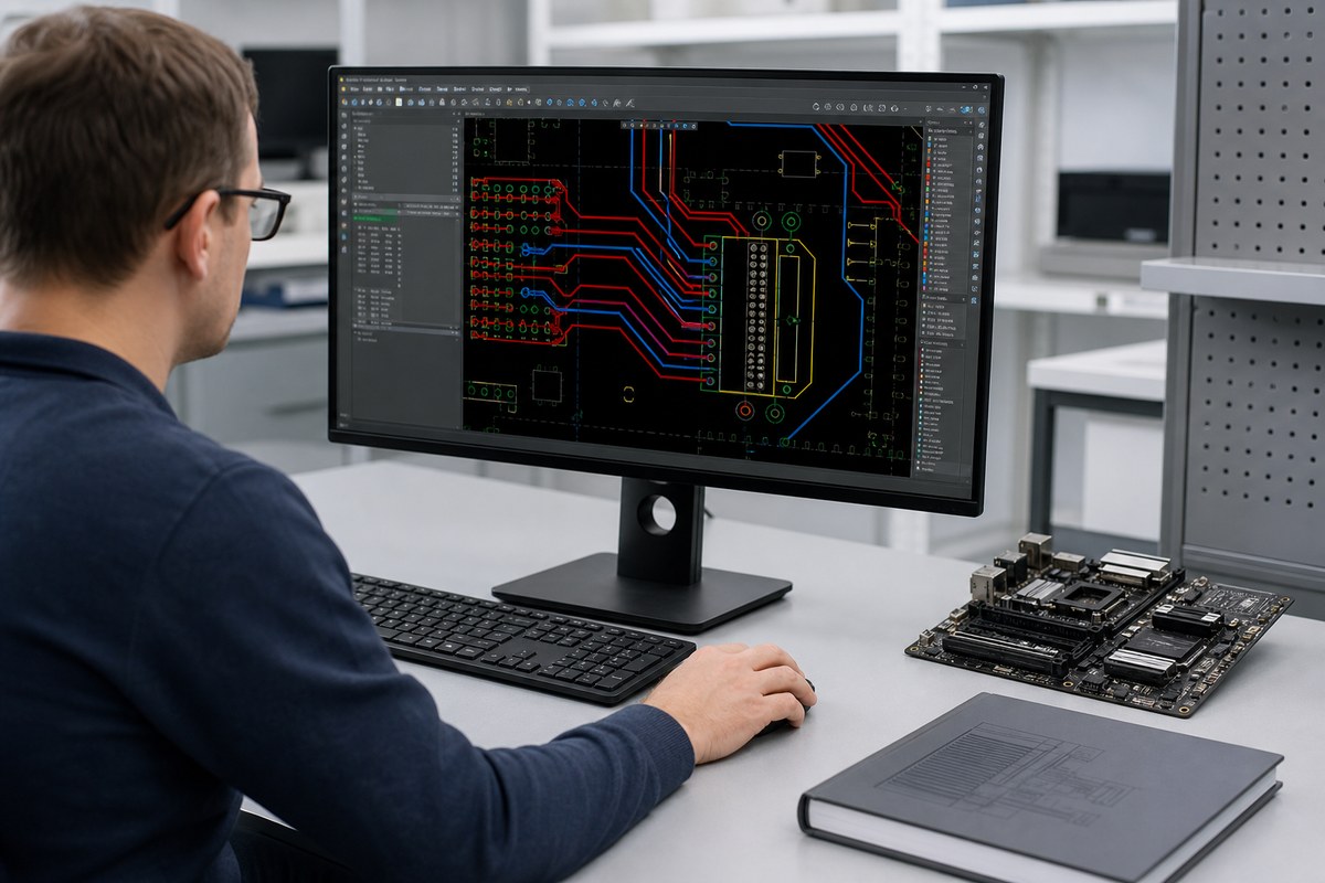
A correct schematic can still fail if the footprint is mirrored, library pins disagree, the connector hits the enclosure, or high-speed pairs cross a plane split. Review logical pin assignment and physical implementation together.
Key checks include:
- Library verification: compare the schematic symbol, footprint, 3D model, and manufacturer drawing pin by pin.
- Orientation control: show pin 1, key position, connector opening, cable exit, and inspection view on the assembly drawing.
- Routing continuity: keep each differential pair together and review layer changes, return vias, stubs, and plane transitions.
- Power protection: confirm the customer-approved fuse or switch, current limit, ESD network, decoupling, and grounding implementation.
- Manufacturing clearance: verify annular ring or pad geometry, solder-mask dam, paste opening where applicable, courtyard, edge clearance, and rework access.
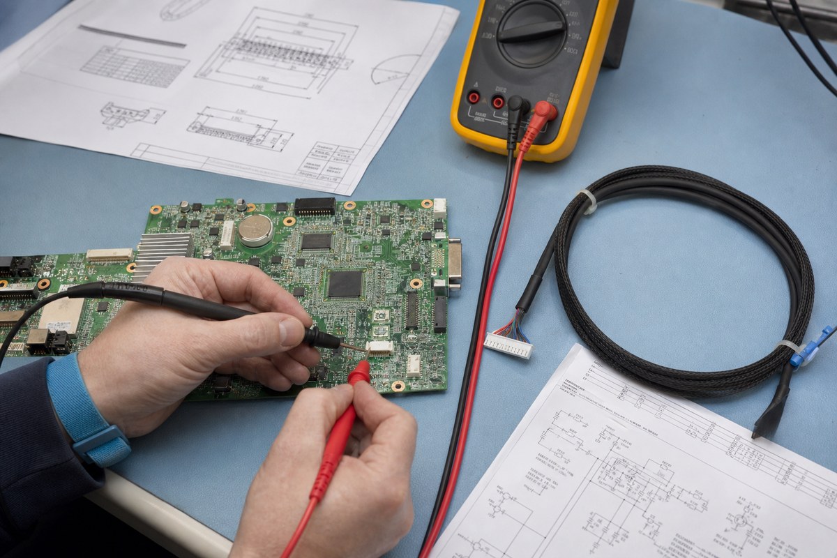
- Test definition: identify accessible checks for continuity, shorts, power rails, connector orientation, and any approved functional fixture.
Release only a matched file set. A corrected assembly PDF cannot compensate for an old Gerber, centroid file, or BOM.
A USB Header PCBA Project Example
A representative USB header PCBA project involved an industrial controller board with conflicting connector, cable, and PCB release files.
Project background
An industrial-equipment team was preparing a pilot controller board. A keyed 2 x 5 USB 2.0 header served an internal touch display and a service port, but the BOM, connector drawing, cable drawing, footprint, and enclosure model came from different revisions.
What the pre-production review found
- The schematic used a top view; the cable drawing showed the mating face without naming the view.
- The generic BOM entry did not define the key position, height, or approved part number.
- Pin 1 was marked on the PCB, but the mark would be partly hidden after the connector was installed, leaving assembly operators without a clear orientation reference.
- The cable exit faced the enclosure wall, limiting insertion and bend clearance.
Actions and outcome
- Purchasing waited for one controlled drawing that aligned pin numbers, mating view, wire map, and part number.
- The keepout and nearby placement were adjusted for installation and cable bend.
- Inspection added orientation and continuity checks; functional testing added enumeration on both ports.
After the files were aligned, the pilot build used one approved connector and one cable orientation. The review prevented reversed installation, enclosure rework, and USB enumeration failures during validation.
Files to Confirm Before PCB Fabrication and Assembly
A revision-controlled RFQ package reduces clarification and ensures suppliers quote the same USB interface.
Provide these inputs when applicable:
- Fabrication data, drills, stackup, impedance requirements, and fabrication drawing.
- Centroid data, assembly drawing, orientation notes, and panel requirements.
- BOM with approved part numbers, alternates, and the exact USB header.
- Schematic and controlled interface drawing.
- Mating-cable drawing and enclosure/3D data when fit is critical.
- Customer-approved inspection, functional test, fixture, firmware, and acceptance requirements.
Before production, withdraw obsolete files and confirm one revision across the release package. Update the full set when the connector or pin map changes.
FAQs About USB Motherboard Pinout
Is every 9-pin USB 2.0 motherboard header wired the same?
No. Many boards follow a common dual-port arrangement, but OEM or custom boards may use different keying or assignments. Verify the exact motherboard manual, board revision, connector drawing, and mating cable.
Can wire color confirm a USB motherboard pinout?
Wire color is only a clue. Confirm continuity and the released pin map because custom harnesses may not use the familiar red, white, green, and black convention.
Why does a USB 3.x motherboard header have more pins?
It commonly carries USB 2.0 compatibility signals plus dedicated SuperSpeed transmit and receive pairs, power, ground, and shielding or drain connections.
Can a USB 3.x header be adapted to a USB 2.0 front-panel cable?
An adapter may provide mechanical and signal conversion for a defined application, but it does not guarantee speed, power, controller support, or correct wiring. Check both specifications and the adapter pin map.
What should a PCB supplier receive to verify a USB header build?
Provide the controlled fabrication and assembly package, BOM, connector part number, schematic or interface drawing, mating-cable information, and customer-approved inspection and test requirements.
Need a pre-production review or quotation for a PCB or PCBA with a USB motherboard pinout? Email your fabrication data, BOM, connector and cable drawings, and test requirements to sales@bestpcbs.com. EBest Circuit can review the package before fabrication and assembly.