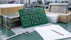
Transparent PCB is used when the circuit board itself needs to support visual inspection, light transmission, compact appearance, or optical product integration. It can appear in display modules, LED products, wearable electronics, sensors, medical devices, automotive lighting, transparent touch interfaces, and demonstration electronics.
For buyers and engineers, the real question is not only “Can the PCB be transparent?” It is also “Can the transparent PCB board be manufactured, assembled, inspected, and delivered without scratches, residue, soldering problems, or material mismatch?” EBest Circuit (Best Technology) supports custom PCB, FPC, special PCB, component sourcing, SMT assembly, inspection, and small-batch PCBA projects. If your project involves transparent PCB, transparent FPC, clear PCB board, or special optical electronics, please send your Gerber files, stackup, BOM, drawing, material notes, and assembly requirements to sales@bestpcbs.com for engineering review before production.

What Is a Transparent PCB?
A transparent PCB is a printed circuit board made with a clear or semi-transparent substrate instead of a normal opaque FR4 board. The purpose is to let light pass through the board or allow the internal circuit structure to remain visible.
A transparent PCB may be rigid or flexible, depending on the material and product structure. It may use transparent flexible film, transparent rigid substrate, transparent polyimide, PET, or selected glass-based circuit substrates for special optical electronics. The copper traces, pads, solder joints, and components are usually still visible, so the finished board is not “invisible.” It is more accurate to describe it as a clear or light-transmitting circuit board.
A transparent PCB project usually needs attention to:
- Optical clarity
- Material transmittance
- Copper pattern visibility
- Surface scratches
- Solder mask choice
- Adhesion reliability
- SMT assembly compatibility
- Residue after cleaning
- Handling and packing protection
For simple display samples, appearance may be the main concern. For functional electronics, the board must also meet electrical, mechanical, thermal, and assembly requirements.
Transparent PCB Board Materials
Transparent PCB board performance depends heavily on material choice. Different materials have different transparency, flexibility, heat resistance, cost, process difficulty, and assembly limits.
Common material options include:
| Material | Typical Use |
| PET | Cost-sensitive transparent flexible circuits |
| Transparent PI | Higher-temperature flexible circuits |
| Clear rigid substrate | Transparent rigid PCB applications |
| Glass-based substrate | Optical, display, sensor, or special transparent electronics |
| Transparent ceramic substrate | Selected optical and thermal applications |
| Acrylic or PC-based materials | Selected display or structural electronics |
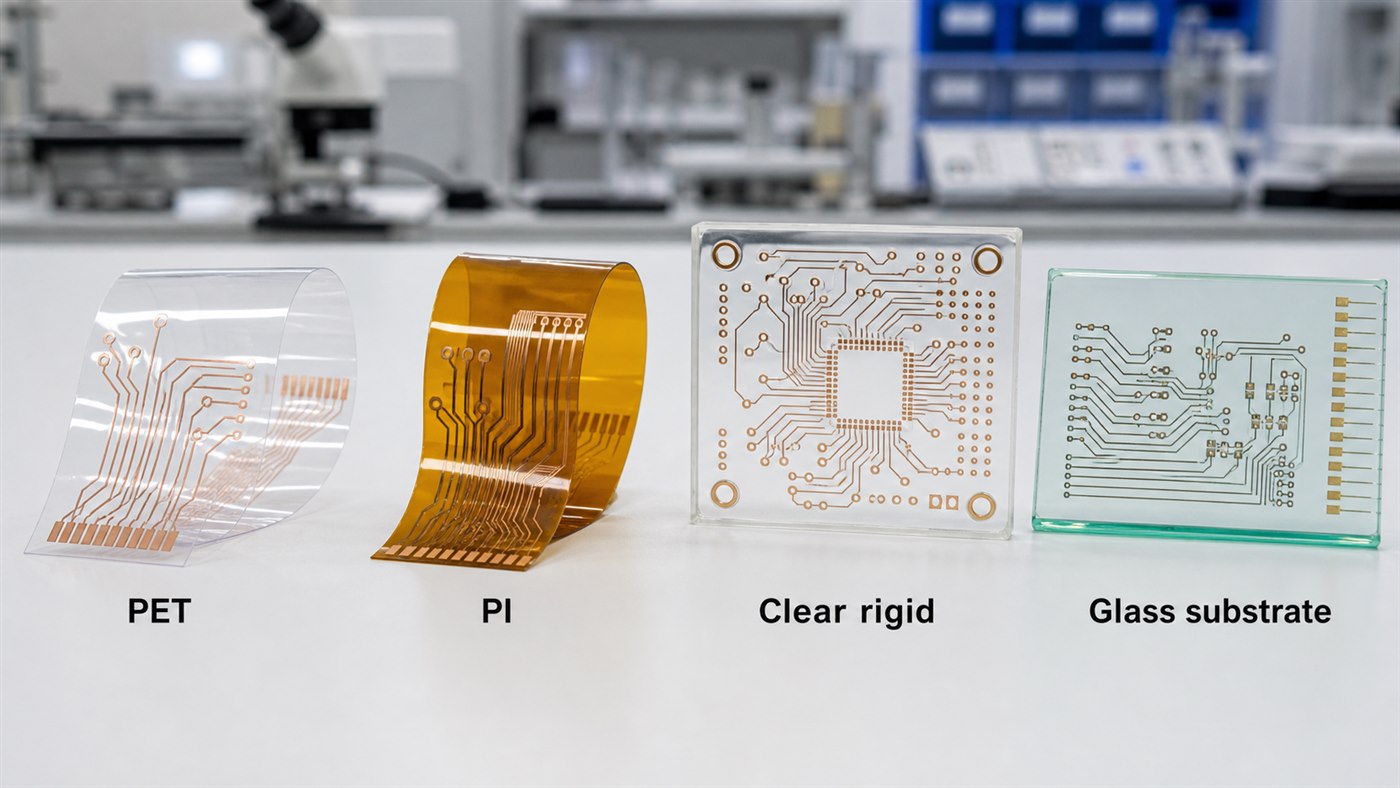
PET may be useful for low-cost transparent flexible circuits, but its heat resistance and SMT process window must be checked carefully. Transparent PI can offer better temperature performance than PET in some applications. Clear rigid substrates may be suitable when the project needs a board-like structure with visible circuitry.
Glass-based circuit substrates and transparent ceramic substrates are more specialized. They should not be treated like standard FR4 PCB materials. They may be considered for optical, display, sensor, LED, or special transparent electronics projects, but manufacturing feasibility depends on substrate type, metallization, drilling or interconnection method, assembly process, and inspection requirement.
For purchasing, the material name alone is not enough. The project should define transparency target, board thickness, copper thickness, temperature requirement, bending requirement, surface finish, assembly method, and visual acceptance standard.
Transparent Circuit Board vs Clear PCB Board
A transparent circuit board and a clear PCB board are often used to describe similar products, but the wording may reflect different customer expectations.
| Term | Common Meaning |
| Transparent circuit board | Focuses on circuit visibility and light transmission |
| Clear PCB board | Focuses on clear substrate appearance |
| Transparent PCB | General search term for transparent printed circuit boards |
| PCB transparent | Search variation used by buyers or engineers |
| Clear PCB | Shorter phrase for transparent-looking PCB |
In real manufacturing, the important point is not the name. The important point is the required function.
Before production, the supplier should confirm:
- Is the board mainly for appearance or optical function?
- Does the board need to transmit light evenly?
- Will it be bent or kept rigid?
- Does it need SMT assembly?
- What surface finish is required?
- Are scratches, haze, or residue unacceptable?
- Will the product be used near heat, light, moisture, or vibration?
A board used in a transparent display module has different priorities from a board used in a wearable sensor, LED lighting product, or demonstration device.
Transparent Flex PCB and Transparent FPC
Transparent flex PCB, also called transparent FPC, is one of the most practical transparent circuit formats. It is usually used when the product needs both circuit connection and flexibility.
Transparent FPC may be used in wearable electronics, transparent touch modules, display connections, medical sensors, LED light strips, flexible user interfaces, automotive lighting, and compact optical modules.
The key advantage is flexibility. The challenge is that transparent flexible materials can be more sensitive to heat, handling, scratches, bending radius, adhesive choice, and surface contamination.
For transparent FPC review, useful checks include:
- Film thickness
- Copper thickness
- Bend area
- Stiffener requirement
- Connector area reinforcement
- Coverlay or insulation opening
- Surface finish
- SMT temperature compatibility
- Final packing method
If the transparent FPC needs components assembled on it, the SMT process must be reviewed carefully. Reflow temperature, solder paste, component weight, panel design, and fixture support can affect yield. For projects that require assembly on flexible circuits, flex PCB assembly review is especially useful before production.
Transparent Rigid PCB Manufacturing Checks
Transparent rigid PCB projects are different from standard FR4 boards. The board may need a transparent rigid substrate, special solder mask, controlled appearance, and careful handling through fabrication and assembly.
Important manufacturing checks include:
- Substrate transparency
- Board thickness tolerance
- Copper adhesion
- Trace and spacing capability
- Via drilling and plating
- Surface finish compatibility
- Solder mask transparency or opening design
- Silkscreen visibility
- Warpage control
- Edge quality
- Scratch prevention
For normal FR4 boards, a minor cosmetic mark may not matter much. For a transparent PCB board, visual defects are easier to notice. Scratches, fingerprints, haze, flux residue, and uneven solder mask can become customer-facing quality issues.
That means the inspection plan should include both electrical performance and appearance requirements.
PET, Transparent PI, and Glass-Based Circuit Substrates
PET, transparent PI, clear rigid substrate, and glass-based circuit substrates are not interchangeable. They serve different product needs.
Material choice should follow the real application:
- Use PET when cost, flexibility, and light transparency are the main priorities.
- Use transparent PI when better heat resistance or flexible circuit reliability is needed.
- Use clear rigid substrate when the product needs a board-like structure with visible circuitry.
- Consider glass-based circuit substrates only when optical stability, flatness, display integration, or special transparent electronics requirements justify a different manufacturing route.
- Consider transparent ceramic substrate only when the project has both optical and thermal requirements and the manufacturing process is confirmed.
The biggest mistake is choosing a material only because it looks clear. A transparent PCB still needs to survive fabrication, assembly, testing, shipping, and real product use.
For example, if the product needs SMT assembly, the material must tolerate the soldering process. If the product needs bending, a glass-based substrate is not suitable. If the product must manage heat, PET may not be enough. If the board is part of an optical product, haze, reflection, scratches, and surface cleanliness may matter as much as electrical performance.
SMT Assembly for Transparent PCB Projects
SMT assembly for transparent PCB projects needs more care than many standard boards because appearance and function are both visible.

Assembly risks include:
- Flux residue on clear areas
- Solder balls near optical zones
- Scratches during handling
- Component skew
- Poor wetting on special pads
- Material deformation during reflow
- Connector stress
- Cleaning marks
- Packing damage
For transparent FPC or thin transparent boards, panel support is especially important. The board may need a carrier, fixture, stiffener, or custom panel design to keep it stable during printing, placement, reflow, and inspection.
EBest Circuit can review:
- BOM and component availability
- SMT temperature compatibility
- Panelization
- Fiducial marks
- Stencil and solder paste requirements
- Connector assembly method
- Cleaning requirement
- Visual inspection standard
- Individual packing needs
The goal is to keep the approved transparent area clean and protect the board from avoidable assembly damage.
Transparent PCB Applications in Electronics
Transparent PCB applications are usually found where appearance, light transmission, compact structure, or optical integration matters.
Common applications include transparent display modules, LED lighting products, wearable electronics, medical sensor devices, smart glass modules, automotive lighting and indicators, consumer electronics prototypes, touch panels, optical sensors, and educational or demonstration electronics.
For buyers, the application should guide the manufacturing decision. A transparent LED product may care about light uniformity and heat. A wearable product may care about bending and skin-contact reliability. A sensor module may care about cleanliness and optical interference. A display-related project may care about haze, scratches, alignment, and visual appearance.
This is why transparent PCB manufacturing should not be quoted only by board size and layer count. The supplier should understand how the board will be used.
Transparent PCB Manufacturing Case Study
A European customer needed a small-batch transparent FPC prototype for a smart display module. The product required a visible circuit area, a flexible connection section, and SMT assembly for several small components.
Project requirements:
- Customer region: Europe
- Application: Smart display module
- PCB type: Transparent flexible circuit
- Quantity: Prototype and small-batch validation
- Key concern: Appearance, flexibility, soldering reliability, and clean delivery
- Assembly need: SMT components and connector area reinforcement
- Packing need: Individual protection to avoid scratches
Main challenges:
- The clear circuit area had to remain clean after SMT.
- The flexible section needed stable bending performance.
- The connector area required reinforcement.
- The customer needed samples for appearance and function review.
- Flux residue and handling marks could affect customer approval.
EBest Circuit review process:
- Checked the Gerber, outline, connector area, and flexible section.
- Reviewed the material and thickness against the bending requirement.
- Confirmed the SMT process window before assembly.
- Planned panel support to reduce deformation during placement.
- Paid attention to cleaning, visual inspection, and packing.
- Protected finished boards individually before shipment.
Result:
The customer received transparent FPC samples suitable for display-module validation. The value was not only making a clear circuit board. The value was keeping the material, SMT process, connector area, appearance requirement, and packing method connected from file review to delivery.
For transparent PCB projects, this kind of early review matters because many problems are difficult to fix after assembly.
FAQs About Transparent PCB
- What is a transparent PCB?
A transparent PCB is a printed circuit board made with a clear or light-transmitting substrate. It may be rigid or flexible, depending on the material and product use. - What is the difference between transparent PCB and transparent FPC?
Transparent PCB is the general term. Transparent FPC usually refers to a flexible transparent circuit made with transparent film materials such as PET or transparent PI. - Can transparent PCB support SMT assembly?
Some transparent PCB and transparent FPC projects can support SMT assembly, but the material, reflow temperature, panel support, surface finish, and cleaning requirement must be reviewed before production. - Is transparent PCB the same as glass PCB?
No. Glass-based circuit substrates are one possible option for special optical or transparent electronics, but they are different from standard FR4 PCB and transparent FPC manufacturing. - What should I send for a transparent PCB quotation?
Send Gerber files, stackup or material requirement, board thickness, copper thickness, transparency requirement, BOM, assembly files, drawing, quantity, and any appearance or packing notes.
All in all, a transparent PCB project needs more than a clear substrate. It needs the right material, controlled manufacturing, clean assembly, careful inspection, and protective packing. If your project involves transparent PCB board, transparent FPC, clear PCB board, or optical electronics PCBA, please send your files and requirements to sales@bestpcbs.com. EBest Circuit can help review the manufacturing path before your project moves into production.