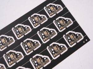
Technical drawings and schematic documents describe different sides of an engineering design. A schematic shows how a system works and how its components connect electrically. A technical drawing defines physical details such as dimensions, materials, hole sizes, tolerances, and assembly orientation.
PCB projects normally need both kinds of information plus machine-readable manufacturing data. This guide explains their differences, how to read them, and what to release so a fabricator or assembler can build the intended revision without guessing.
What Are Technical Drawings?
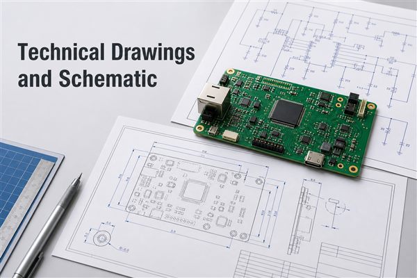
Technical drawings are controlled documents that communicate the physical requirements needed to make, assemble, or inspect a product. They use views, dimensions, notes, symbols, callouts, and revision information rather than relying on a realistic picture alone.
In a PCB project, the term can include several different documents:
- Fabrication drawing: board outline, dimensions, holes, stackup, tolerances, notes, and special process requirements.
- Assembly drawing: component locations, reference designators, polarity, orientation, and assembly-side information.
- Mechanical drawing: enclosure interfaces, connector positions, keep-out areas, mounting features, and fit requirements.
- Inspection drawing: dimensions or characteristics that must be measured and recorded.
The search phrase technical drawings explained often leads to a simple idea: a drawing should let another qualified person interpret the physical design consistently, including the units, scale, tolerances, and revision.
What Are Schematic Drawings?
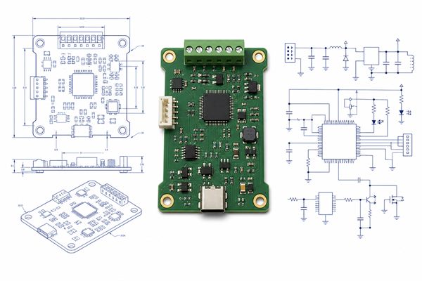
Schematic drawings represent functional relationships rather than physical shape or placement. In electronics, a schematic uses standardized symbols and named nets to show which component pins are connected and how the circuit is intended to operate.
A resistor symbol does not show the resistor’s package size, color, or exact board location. Likewise, two parts drawn next to each other may be far apart on the finished PCB. The diagram is organized for electrical understanding, not spatial accuracy.
For readers looking for a concise schematic drawings definition, a schematic is an abstract map of system function and connectivity. Our guide to reading a circuit diagram schematic explains symbols, reference designators, nets, and signal flow in more detail.
What Is the Difference Between a Technical Drawing and a Schematic?
The main difference is the question each document answers: a schematic explains what connects and how the circuit functions, while a technical drawing explains what the physical product must be.
| Document | Primary Purpose | Typical PCB Information |
|---|---|---|
| Schematic | Electrical function and connectivity | Symbols, pin numbers, net names, values, power rails |
| Fabrication drawing | Bare-board physical requirements | Outline, holes, stackup, tolerances, notes |
| Assembly drawing | Component placement and orientation | Reference designators, polarity, side, special instructions |
| Mechanical drawing | Fit and interface control | Mounting, connector, enclosure, and keep-out geometry |
These documents complement one another. A manufacturer should not have to infer drill tolerances from a schematic or guess component polarity from a bare-board outline.
Which Technical Drawings and Diagrams Are Used in PCB Projects?
The necessary technical drawings and diagrams depend on whether the supplier will fabricate a bare board, assemble components, or deliver a tested PCBA. A complete release may contain the following document groups:
- Electrical design: schematic PDF and native design files when design support is required.
- Bare-board fabrication: Gerber or ODB++ data, NC drill files, fabrication drawing, stackup, and controlled-impedance requirements.
- Assembly: BOM, centroid or pick-and-place file, assembly drawing, approved substitutions, and special process notes.
- Mechanical integration: board outline, 3D model, enclosure drawing, connector datums, and height restrictions.
- Test and inspection: test-point information, programming requirements, acceptance criteria, and test procedure where applicable.
A PDF helps people review the release, but machine-readable data drives many production operations. Our overview of Gerber files in PCB manufacturing explains how plotted board layers differ from a general technical drawing.
Reading Technical Drawings and Schematics
Reading technical drawings and schematics is easier when you first identify the document’s purpose, revision, units, and reference system. Do not begin by interpreting isolated symbols or dimensions before confirming that the sheets belong to the same release.
- Check the title block. Confirm the document number, revision, date, units, scale, sheet number, and approval state.
- Read the notes and legend. General notes can control material, finish, workmanship, and inspection even when no arrow points to them.
- Identify the reference system. A schematic uses reference designators and net names; a mechanical drawing uses datums, coordinates, and dimensions.
- Trace one functional path at a time. Follow power, ground, inputs, outputs, and interfaces rather than trying to decode the full schematic at once.
- Cross-check linked files. Match reference designators to the BOM and assembly drawing, then compare board geometry with the fabrication data.
- Record uncertainties. Raise a documented engineering question instead of choosing an unapproved interpretation.
How Does a Schematic Become a PCB Layout?
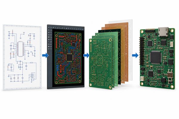
A schematic becomes a PCB layout after its logical components and nets are assigned physical footprints, placed on a board outline, and connected with routed copper. The PCB layout is therefore a physical implementation of the schematic, not a replacement for it.
The transfer typically follows this sequence:
- Validate component symbols, pin numbers, values, and electrical rules.
- Assign the correct footprint and package to every fitted component.
- Import or update the schematic connectivity in the PCB layout tool.
- Define the board outline, layer stack, design rules, and mechanical constraints.
- Place components according to electrical, thermal, mechanical, and assembly needs.
- Route traces and planes, then run electrical and design-rule checks.
- Release fabrication and assembly outputs from the approved source revision.
Pin mapping is a critical transition point. A correct circuit symbol paired with the wrong footprint can produce a board that passes schematic review but connects the physical component incorrectly.
Which Technical Drawings Belong in a PCB Fabrication Package?
A PCB fabrication package should include a controlled fabrication drawing plus the machine-readable files needed to create the bare board. The drawing should communicate requirements that are not safely conveyed by plotted copper and drill data alone.
Common fabrication-drawing content includes:
- Finished board dimensions, outline tolerances, cutouts, slots, and edge details.
- Finished hole sizes, plated and non-plated hole identification, and special tolerances.
- Layer count, stackup requirements, copper weight, finished thickness, and material notes.
- Surface finish, solder mask, legend, edge plating, controlled depth, or other special processes.
- Controlled-impedance targets and coupon requirements when applicable.
- Panelization or breakaway requirements when they are controlled by the customer.
- Document number, revision, units, and applicable acceptance requirements.
The fabrication drawing should agree with the Gerber or ODB++ data and NC drill files. A drawing can define the finished diameter and tolerance, while the drill data identifies each hole location. Our PCB design for manufacturability guide covers the DFM checks that connect design intent to stable production.
Which Documents Belong in a PCB Assembly Package?
A PCB assembly package should identify what to place, where to place it, how to orient it, and which build revision is approved. The core release normally combines a BOM, centroid data, assembly drawings, and applicable process or test instructions.
| File | Core Information | Key Cross-Check |
|---|---|---|
| BOM | Part numbers, values, quantities, reference designators | Designators and fitted status match the approved design |
| Pick-and-place | Component coordinates, rotation, and board side | Origin and rotation convention are defined |
| Assembly drawing | Locations, polarity, orientation, and special notes | Visual orientation agrees with centroid data |
| Test or programming instruction | Procedure, limits, fixtures, firmware, and records | Instruction revision matches the assembly revision |
Do-not-fit parts must be handled consistently across the BOM, assembly drawing, and placement data. A note on one file is not enough if another release file still tells production to install the component. See our PCBA manufacturing process guide for how these inputs support sourcing, placement, soldering, inspection, and testing.
What Happens When Drawings and Manufacturing Data Conflict?
When released files conflict, production should stop at the affected requirement and obtain a documented clarification. Choosing one source without an agreed precedence can create a repeatable but incorrect build.
Typical conflicts include:
- The fabrication drawing specifies a board thickness that differs from the stackup file.
- The BOM revision does not match the schematic or assembly drawing revision.
- A component is marked do-not-fit in one document but appears in the pick-and-place file.
- Polarity shown on the assembly drawing disagrees with the footprint or centroid rotation.
- The mechanical drawing and Gerber outline contain different dimensions.
A release note or document index should state the governing revision and file set. The approved response to an engineering query should then be retained with the job record so purchasing, fabrication, assembly, inspection, and future repeat orders use the same decision.

What Common Drawing Errors Delay PCB Manufacturing?
The most disruptive drawing errors are usually mismatches, missing controls, or ambiguous notes rather than visual imperfections. They force the manufacturer to pause and ask which interpretation is correct.
- Mixed revisions: files exported on different dates or from different source revisions.
- Missing units or tolerances: dimensions exist, but the acceptable manufacturing range is unclear.
- Undefined slots and cutouts: geometry appears in one layer without clear finished size or plating status.
- Incomplete stackup: layer order, finished thickness, copper requirements, or impedance construction is not controlled.
- BOM and designator mismatch: quantities and component locations cannot be reconciled.
- Unclear polarity: the schematic, footprint, assembly drawing, and component datasheet do not agree.
- Uncontrolled notes: copied legacy instructions contradict the current files.
- Illegible output: text, line weights, or plotted layers become unreadable in the released PDF.
A release review should compare documents against one another, not merely confirm that every expected filename exists.
How Should You Prepare a Build-Ready PCB Document Set?
A build-ready document set should be exported from one approved source revision, named consistently, and checked as a complete package before it is sent. The goal is to make the design intent unambiguous to both engineers and production systems.
- Freeze the approved schematic and PCB source revision.
- Run schematic, electrical-rule, and PCB design-rule checks.
- Regenerate fabrication and assembly outputs from that same revision.
- Open the released Gerber or ODB++ data in an independent viewer.
- Compare the drill data, outline, stackup, dimensions, and impedance notes.
- Cross-check the BOM, reference designators, polarity, centroid coordinates, and do-not-fit status.
- Include a release index that lists the current files and revisions.
- Remove superseded output from the delivery package so it cannot be selected accidentally.
Use the second occurrence of technical drawings and schematic as a final review concept: logical intent, physical requirements, and production data must describe the same board.
FAQ About Technical Drawings and Schematics
Is a schematic the same as a blueprint?
No. A schematic is an abstract functional diagram, while “blueprint” is an informal term often used for a physical plan or technical drawing. The exact document type matters more than the casual label.
Does a schematic show physical component placement?
No. A schematic may group related functions for readability, but it does not define where components sit on the PCB. Placement belongs to the PCB layout and assembly data.
Can a PCB be manufactured from a schematic alone?
No. A schematic does not define the complete board outline, routed copper, layer data, drill coordinates, solder mask, legend, or other fabrication outputs needed to manufacture the bare PCB.
What is the difference between a schematic and a wiring diagram?
A schematic emphasizes circuit function using symbols and logical connections. A wiring diagram generally shows more practical connection detail, such as wires, terminals, connectors, or harness routing.
What file shows a PCB’s drill sizes?
NC drill data provides hole locations and tool information, while the fabrication drawing can specify finished-hole requirements, plating status, and tolerances. Both should be reviewed together.
Should a fabrication drawing include dimensions?
Yes. It should include the controlled board dimensions and critical mechanical features that cannot be left to interpretation. The drawing should also identify units and tolerances.
What does an assembly drawing show?
It shows component locations, reference designators, board side, orientation, polarity, and special assembly instructions. It works with the BOM and pick-and-place file rather than replacing them.
Why do reference designators need to match the BOM?
Matching designators connect each BOM line to a specific placement location. A mismatch can cause missing parts, incorrect quantities, unresolved substitutions, or assembly delays.
Which revision should a manufacturer follow?
The manufacturer should follow the revision explicitly approved in the release package or purchase documentation. If the supplied files contain mixed revisions, the conflict must be clarified before production.
Are PDF drawings enough for PCB production?
Usually not. PDFs are useful for human-readable drawings and notes, but PCB fabrication and assembly also require appropriate machine-readable layer, drill, placement, and procurement data.
How Can EBest Circuit Support a Document-Ready PCB Project?
At EBest Circuit, we support PCB fabrication and PCBA projects by reviewing the supplied design package before production and raising clear engineering questions when files are incomplete or inconsistent. This helps align the schematic, fabrication requirements, assembly data, and approved revision before materials and manufacturing steps are committed.
Send your Gerber or ODB++ data, NC drill files, fabrication drawing, BOM, pick-and-place file, assembly drawing, quantity, and test requirements to sales@bestpcbs.com. We will review the package and discuss the next steps for your PCB or PCBA project.