Two coplanar waveguide calculators give you different widths for 50 Ω? First check which one includes copper beneath the trace. Then compare the actual dielectric height, the gap on each side, finished copper thickness, and solder mask. Don’t change the dielectric constant just to make the answers agree.
Here’s how to work through a 50 Ω RF feed from the layer drawing to the impedance report. You’ll see how much a model change can move the answer, which dimensions to confirm with the PCB shop, and what a passing coupon still can’t tell you.
What Is Coplanar Waveguide?
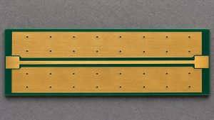
A coplanar waveguide (CPW) has a signal trace and ground copper on either side of it, all on the same layer. If there is also a continuous reference plane underneath and the side grounds connect to it, choose the grounded CPW model, also called GCPW, CPWG, or conductor-backed CPW. Different software uses different names. Check the little cross-section on the input screen rather than going by the name alone.
A dimension that matters here is H: the dielectric height from the signal-layer copper to its reference copper. If L1 routes over a solid L2 plane, this is the L1–L2 dielectric height, not the thickness of the board. If L2 has a cutout under the feed, one uniform model no longer represents the whole path.
Coplanar Waveguide vs Microstrip: Which Model Should You Use?
Look at what the fields can couple to. A plain microstrip model accounts for a trace over a plane but not for close side copper. A plain CPW model accounts for the side copper but not for a backing plane. The grounded model accounts for both. Once you’ve picked the model, use the same finished cross-section in both tools.
| Model | Use when | What makes it the wrong choice |
| Microstrip | A solid plane sits below the feed; side copper is far enough away to have little effect. | Nearby side pours materially change the impedance in a sensitivity check. |
| CPW | The two top-side grounds set the reference and there is no backing plane in the modeled section. | A nearby plane below the feed carries part of the return current. |
| Grounded CPW | The feed has nearby side grounds tied to a continuous reference plane underneath. | A ground cutout, floating pour, or isolated launch feature breaks those assumptions locally. |
If you’re not sure the side copper can be ignored, solve once with it and once without it. Compare the difference with your project’s impedance budget. That’s a better test than borrowing a fixed gap-to-height rule from a different board. See the separate CPW vs GCPW model guide for grounds and return paths.
Grounded Coplanar Waveguide Impedance: What to Enter
Get the dimensions from the fabricator’s proposed finished stackup. Nominal foil thickness and the dimensions in the CAD editor answer different questions from finished copper thickness and etched line geometry.
| Input | Example worksheet | What to confirm before release |
| W, signal width | 0.30 mm | Finished width convention: top, bottom, or average for a trapezoidal trace. |
| G, one side gap | 0.15 mm per side | Edge-to-edge from the signal to one adjacent ground, not 0.30 mm total across both gaps. |
| H, dielectric height | 0.18 mm | Finished L1–L2 dielectric thickness, not total board thickness or an unpressed prepreg value. |
| εr, relative permittivity | 4.0; assumed | Agreed laminate model, Dk basis and frequency. Do not substitute a generic FR-4 value for release. |
| T, copper; mask | 0 mm copper and no mask for the ideal calculation only | Use actual plated thickness and the mask opening or coating over the trace and gaps in the production model. |
When a tool’s description says “substrate height,” check what its sketch measures. For a grounded structure it’s the distance to the backing plane in the illustrated section. If the two etched gaps aren’t equal, don’t silently average them for sign-off. Ask for a solver that can model the actual section, or agree a conservative range with your fabricator.
How to Use a Coplanar Waveguide Calculator
- Start in analysis mode. Select the CPW or grounded CPW cross-section. Enter a known width and gap and calculate impedance. Use the same units and stackup in both tools.
- Resolve differences one input at a time. Check backing copper and H first, then gap definition, copper, mask and Dk. Record the setting that moved the answer. If a model can’t represent a key feature, note the omission rather than tuning Dk to hide it.
- Use synthesis for a candidate layout. Fix a gap the shop can hold, set the target impedance and solve for width. Run analysis again using the rounded width you’d actually route. The KiCad transmission-line calculator documentation describes analysis and synthesis and lists both types of CPW.
- Ask what can move in production. Agree which dimensions can be compensated and which are fixed by the launch or clearance rules. Compare minimum and maximum inputs supported by the selected process. Document the revision and measurement scope before ordering.
If different tools still disagree after aligning the cross-sections, compare their treatment of copper thickness, mask and dispersion. Use a 2D solver for a uniform printed section. A connector pad, reference-plane slot or abrupt taper is a different problem: evaluate those transitions with an appropriate 3D model or a calibrated RF measurement when performance depends on them.
Coplanar Waveguide Impedance Formula: A Worked Check
Here’s a calculation you can repeat. Use the worksheet geometry and first set conductor thickness to zero and remove mask. This ideal, quasi-static comparison isolates the effect of backing copper; it is not a fabrication recipe. In the grounded model, let k = W/(W + 2G) and kb = tanh(πW/4H)/tanh[π(W + 2G)/4H]. Define Q(x) = K(x)/K(√(1 − x²)), where K is the complete elliptic integral of the first kind written in terms of its modulus. If your library takes the parameter instead, pass x² to K.
For W = 0.30 mm, G = 0.15 mm and H = 0.18 mm, k = 0.5. Set S = Q(k) + Q(kb). Then εeff = 1 + (εr − 1) × Q(kb)/S, and Z₀ ≈ 188.365/(S√εeff) Ω. This is the ideal grounded branch in the KiCad source implementation, before its thickness, mask and frequency adjustments.
| Change from the worksheet baseline | Calculated Z₀ | What to check |
| Grounded model, unchanged | 53.43 Ω | Use as the comparison baseline, not a finished-board prediction. |
| Switch to the unbacked CPW model | 83.22 Ω | Check the backing plane before changing trace width. |
| Grounded; decrease gap to 0.12 mm | 52.04 Ω | Closer side grounds can lower impedance; check the minimum finished gap. |
| Grounded; increase H to 0.22 mm | 58.00 Ω | Check the proposed pressed dielectric when a material changes. |
| Grounded; narrow width to 0.28 mm | 55.49 Ω | In this section a narrower trace raises impedance; include etch variation. |
For the unbacked comparison, the dielectric slab thickness remains 0.18 mm but there is no metal beneath it. Replace tanh with sinh in the expression for kb to obtain ku. Use εeff = 1 + (εr − 1) × Q(ku)/[2Q(k)] and Z₀ ≈ 94.183/[Q(k)√εeff] Ω. The result jumps nearly 30 Ω without a single change to the top artwork. That doesn’t predict a 30 Ω jump on your board. It shows how a model mismatch can swamp smaller adjustments.
Grounded Coplanar Waveguide Design: From Uniform Trace to Real Board
Divide the route into its uniform line and the nonuniform sections. Use the calculator for the long, straight section you can describe by one cross-section. For the connector launch, component pad or bend, check the actual pad, taper, local gap and plane continuity separately. A wider connector pad typically adds capacitance relative to a narrow uniform feed, but the real transition response also depends on the ground geometry and connector. Don’t copy the uniform-line gap through the launch without checking the transition.
On a prototype, a pass on the coupon and poor return loss at the connector aren’t contradictory. First inspect calibration plane and launch geometry. Compare the response of a representative launch test line, when available, with the functional feed. Don’t conclude the whole trace is wrong from a fixture reflection, or redesign the route solely because the calculator disagrees with the assembly.
Grounded Coplanar Waveguide Via Spacing
Put the return connection where the ground current needs it: next to transitions and along the coupled side grounds, tied to the actual reference plane. A cross-section calculator has no way to represent a missing stitch via by itself. Even if it prints 50 Ω, it does not tell you whether the two top grounds stay effectively at the same potential through the launch or whether the via fence works over your operating band.
Evaluate via-to-trace offset and longitudinal spacing separately. First check the connector footprint, manufacturing clearances and route to the ground plane. Then model or measure the real geometry at the upper end of the required band. If you change fence pitch, compare the same launch and stackup before and after; don’t assign a universal pitch to every material and bandwidth. See the RF via fence and launch guide for the layout side of that check.
PCB Impedance Test Coupon: How to Read the Report
Before judging the number, look for panel and coupon ID, the represented layer and GCPW geometry, target and tolerance, test method and measured interval or result. If the report only says “50 Ω PASS” and doesn’t identify the structure, ask which coupon line was actually tested. A microstrip coupon isn’t direct evidence for a grounded coplanar feed with a different cross-section.
For example, assume your drawing specifies 50 Ω ±5% on an L1/L2 grounded line. That’s 47.5–52.5 Ω, a project requirement, not an IPC default. If a matching coupon reports 51.8 Ω using the agreed method and decision rule, it meets that example numerical window. If the coupon has no geometry identifier or the setup can’t resolve a borderline value with the agreed uncertainty rule, don’t release on the number alone. IPC-TM-650 2.5.5.7, Revision A (March 2004), §1.2 discusses measurement limitations and §3.1.2 describes representative nonfunctional lines. It is a test method; the purchase drawing sets the required target, limits and decision rule.

Release only what the evidence supports: a representative coupon can confirm the uniform line under the agreed test conditions. It doesn’t prove the installed connector’s return loss, insertion loss or broadband behavior. For those, agree a separate VNA measurement and reference plane and compare against the project’s RF limits.
Coplanar Waveguide Calculator FAQs
Why did KiCad and another calculator give different 50 Ω widths?
Start with the cross-section drawings. Match the backing plane, layer-to-plane height and one-sided gap. If those are identical, compare solder mask, finished copper and model assumptions before changing Dk.
Is 0.15 mm the total gap or the gap on each side?
In the symmetric worksheet, it is 0.15 mm per side. The total span across both slots is 0.30 mm, excluding the center trace. Confirm how your particular calculator labels the field.
Can I use 1.6 mm for the dielectric height on a four-layer PCB?
Not if a closer layer is the solid reference plane. Use the finished signal-to-reference dielectric. In the example that is 0.18 mm; the total board thickness can still be much larger.
Should I include solder mask if the connector pads are exposed?
Include it for the covered uniform feed when the solver supports it. Treat the exposed launch as a separate transition; the fact that pads are exposed doesn’t tell you how much mask covers the rest of the line.
Can a 100 Ω differential pair be modeled as two independent 50 Ω lines?
Not when the two signals couple appreciably. Use a differential coplanar cross-section that includes line-to-line spacing, side gaps and the reference plane. Ask for a differential coupon if that’s the purchase requirement.
Can I copy a 50 Ω trace width from an evaluation board?
Use it to understand the reference launch, not as a universal width. Copy the relevant stackup, connector and plane geometry only when they really match; otherwise, recalculate and revalidate.
Does a calculator’s 50 Ω reading guarantee S11?
No. It estimates the characteristic impedance of a uniform model. Measured S11 also includes discontinuities, the launch, termination and the measurement reference plane.
What do I send when the board shop asks which geometry it can adjust?
Send the stackup revision, layer and net class, target and tolerance, routed width and gap, mask opening, and the dimensions that cannot move at the launch. Ask for the proposed finished cross-section before approval.
Technical References
- KiCad Calculator Tools: transmission line models
- KiCad: coplanar calculation implementation and formula references
- IPC-TM-650 2.5.5.7, Revision A: characteristic impedance by TDR
Need a Custom 50 Ω RF PCB? Review the Stackup Before You Order
If your calculator results disagree, send EBest Circuit both cross-sections before you release the artwork. Our controlled-impedance PCB service can review the stackup so there’s a clear definition of the line to manufacture. Ask about a representative TDR coupon so the impedance report can be tied to the layer and structure you ordered.
Email sales@bestpcbs.com for a quote. Include your Gerbers or ODB++ data, stackup, layer pair, target impedance and tolerance. Flag connector-launch dimensions that cannot change so the review can distinguish fixed features from dimensions the shop can adjust.