If a differential TDR trace shows a bump near the launch, put a known reference on the fixture before changing the board. Align when the instrument sees each edge and when the two stimulus edges reach the board. A display shift can line up two saved traces, but it cannot change what was launched into the board.
The practical check is simple: save the acquisition and launch baselines, verify them after reconnecting, and compare the residual on a known reference with the smallest board effect the test needs to resolve. If the reference cannot pass that check, the result is inconclusive, not a board failure.
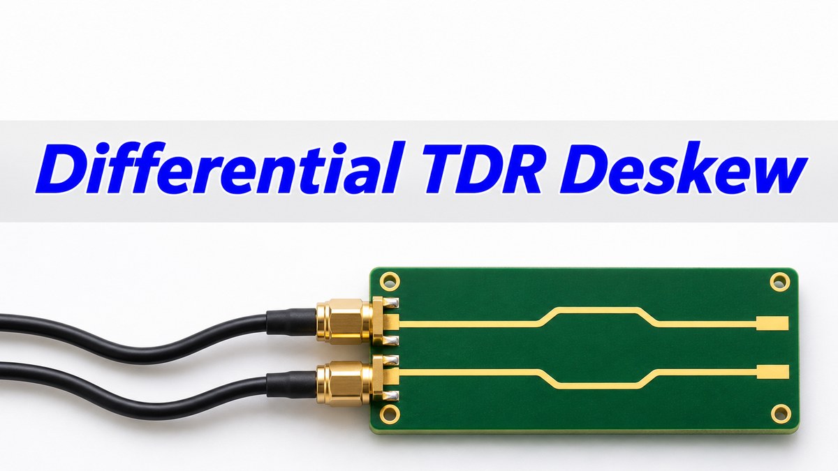
Differential TDR: Check the Setup Before the Board
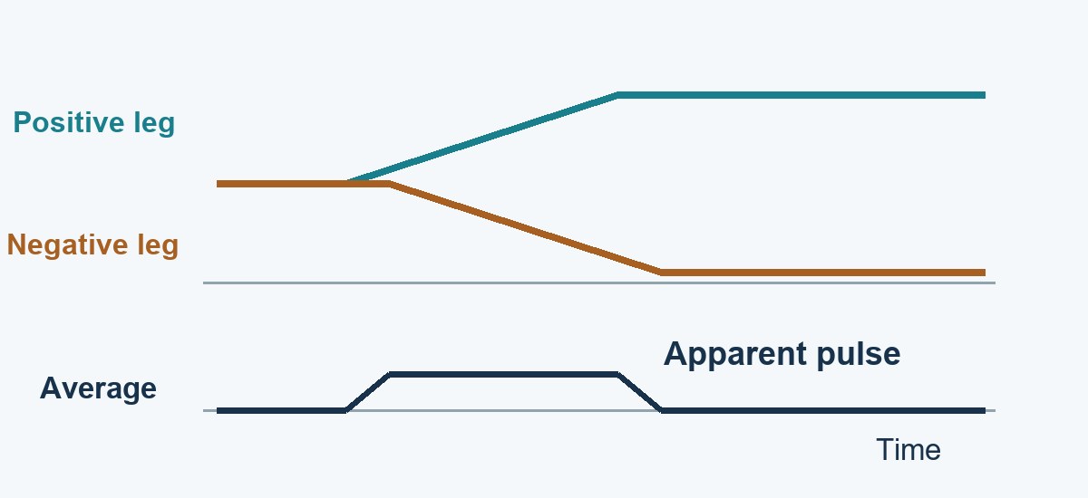
Differential time-domain reflectometry (TDR) drives the two conductors with nominally equal, opposite steps and observes reflections. In a symmetric system, those opposite changes cancel in the common-mode average. If one edge arrives early, the cancellation is incomplete while the edges are changing, even if both paths settle to the expected voltage.
Keep the raw positive and negative leg traces, not just the derived impedance plot. Use the same bandwidth, rise-time setting, fixture, cable orientation and calibration reference for the baseline and board. A stable difference on a board can matter; one already present on a known reference is not evidence against that board.
TDR Calibration: Separate Three Different Corrections
Timing alignment, impedance calibration, and fixture removal solve different problems. Follow the instrument procedure for their order and confirm where its reference plane ends. In a connectorized setup, the end of the test cables and the start of the PCB traces are not necessarily the same plane.
| Correction | What changes | What it cannot prove |
| Acquisition deskew | Accounts for a relative time offset in how the two receive paths record a common timing reference. | Does not make incident edges arrive together at the device under test. |
| Incident step deskew | Changes relative launch timing where the instrument supports actual source delay adjustment. | Does not correct gain mismatch or remove fixture discontinuities. |
| Impedance calibration or fixture removal | Establishes the reference for impedance conversion or removes modeled fixture response, as applicable. | Does not independently prove source and receive timing are matched. |
IPC-TM-650 2.5.5.7A (March 2004) describes characteristic impedance measurement, including a differential measurement process in §5.3. It is not a universal picosecond limit for differential deskew. Use the product test plan and the instrument’s supported alignment routines.
Oscilloscope Deskew: Align the Acquisition Paths
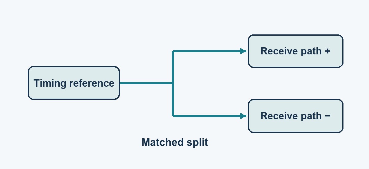
Apply an approved common timing reference to both receive paths at the intended plane. A characterized splitter or a manufacturer’s alignment fixture is useful because an unequal reference cable would otherwise be counted as an instrument error. Keep compatible terminations and reference hardware; do not improvise a connection between independent active outputs.
Measure the same fractional crossing on both edges; use consistent polarity and local amplitudes so offset or amplitude error does not masquerade as time shift. Record the signed difference, channel mapping, reference components, edge setting and repeat spread. If the delay noticeably varies with crossing level, investigate step-shape or bandwidth mismatch; one offset is unlikely to correct the entire edge.
TDR Step Deskew: Align the Incident Edges
With acquisition timing checked, apply the instrument’s incident-step alignment procedure using its approved reference configuration at the selected plane. Set or verify relative launch delay, then save a second baseline. A Keysight FlexDCA system, for example, distinguishes hardware step skew from shifting a waveform on the screen; other instruments can use different procedures or may lack independent launch control.
Do not interpret an open-reference return-time difference as one-way skew unless the instrument method defines that conversion. A reflected edge travels out and back, and the displayed timing can include both acquisition and source corrections. If the instrument cannot align or demonstrate coincident launches, document that limitation rather than tuning the board result into agreement.
Common Mode Voltage: Quantify a Timing Artifact
For equal and opposite steps, the common-mode voltage is the average of the two measured legs. If the only error is a small delay Δt and the edges have similar shape, the magnitude of a local timing artifact is approximately |slope| × |Δt| ÷ 2. This follows from subtracting an edge from a delayed copy before taking the average.
In an illustrative near-linear interval, each leg changes by 0.50 V over 50 ps, a slope of 10 mV/ps. An 8 ps mismatch gives roughly 40 mV of apparent common mode. Reducing the residual mismatch to 2 ps brings the estimate to about 10 mV. That is an edge-window estimate, not a peak guaranteed by the instrument, an impedance in ohms, or a frequency-domain conversion metric. Unequal step heights, baseline error or different edge shapes can leave a residual even at zero timing offset.
TDR Test Fixture: Read the Reference Before Repeating on the Board
Reconnect a suitable known reference after alignment and take enough readings to characterize the setup repeatability. Preserve the same reference plane, attenuation, edge setting and fixture configuration. If changing an adapter changes the timing offset, repeat alignment for that configuration rather than comparing it against the old baseline.
| Observation | What to check next |
| Offset appears on the common timing reference. | Check receiving paths, reference split, and crossing definitions before adjusting source launch timing. |
| Acquisition reference passes, but the known differential reference shows an edge pulse. | Check incident step timing, leg amplitude and shape, and physical fixture symmetry. |
| Known reference passes; the feature repeats only on the board at the same board-referenced location. | Investigate the PCB transition. Record the baseline and attach both raw leg traces before changing the layout. |
A controlled path swap can help: if the apparent difference follows a channel or cable on the reference, the apparatus still contributes. If it follows the same physical board leg after channel identities are restored, investigate that leg. Use documented reconnections; a swap that changes geometry or connector loading is not a clean control.
If the setup is stable and the impedance changes where an otherwise matching route enters a dense or sparse copper region, use the PCB copper density and impedance guide to compare finished trace widths, dielectric spacing and the return path before changing the layout.
If you are verifying the same interconnect in the frequency domain, do not mistake a changed cable pose for a board effect. The VNA cable movement guide separates cable flex from connector remating using a fixed reference.
Differential Pair Skew: Separate Board Delay From Setup Error
For a connector launch, verify the launch reference first, then check that the PCB-only feature stays put when you repeat the setup. For a via transition, hold the edge speed and reference plane constant; a local impedance feature can remain after both channels are aligned. See the PCB via impedance guide for the separate task of identifying that transition.
For incoming coupon reports, ask which reference condition, mode, and measurement window were used before comparing numbers from two labs; the PCB impedance test report checklist covers lot-level traceability. If you actually need board-leg propagation delay from end to end, use a suitable transmission-delay measurement and reference plane. Do not convert every reflection timing difference into a routed length offset.
TDR Measurement Setup: Record a Repeatable Acceptance Check
Start with the smallest relevant board signal and decide how much setup error the measurement can tolerate. For example, if the test plan allows 15 mV of residual edge artifact in a defined window and the relevant slope is 10 mV/ps, a first-order timing budget is about 3 ps, assuming skew is the only contributor. Verify the actual baseline amplitude with the same window; the calculated budget does not cover gain error or ringing.
Use a log with reference ID, both channel/cable IDs, plane, edge setting, raw and corrected offsets, repeat spread and actual baseline residual. Example entry: “Ref A; same launch plane; 8 ps before, 2 ps after; 10 mV baseline measured in the defined window against a 15 mV limit.” This is a hypothetical report entry. Record the offset and residual on each reconnect required by the plan. Hold the judgment if repeatability or the residual is too close to the limit to support it.
Differential TDR Deskew FAQs
Does oscilloscope probe compensation also deskew a channel?
No. Compensation adjusts the probe’s response; deskew corrects relative timing. Both may affect what you see at the edge, so record which procedure was applied.
Can identical cables be assumed to have identical delay?
No. Part tolerances, adapters and routing affect the complete path. Verify the actual pair with the reference connected where you need the alignment.
Is display alignment enough for a true differential launch?
No. Aligning captured traces cannot make the two sources reach the board at the same instant. Verify incident timing separately with the supported procedure.
Does a flat common-mode trace prove the setup is calibrated?
No. It is useful evidence under a defined reference and window. It does not prove absolute impedance accuracy, equal gain at all frequencies, or valid fixture removal.
Should I deskew again after moving a cable?
Recheck the baseline after reconnecting, changing a cable or adapter, or changing settings that affect timing. Repeat formal alignment if the verified residual no longer meets the plan.
Does every differential TDR need 3 ps accuracy?
No. That is an illustrative estimate from a specified slope and voltage budget. Derive your limit from the measured edge and the task’s tolerable artifact.
Can I infer cable length from a TDR time difference?
Only with the propagation velocity and the correct time convention for the setup. A reflected signal generally includes both outbound and return travel.
What if the baseline still shows ringing after alignment?
Check connection quality, reference response, bandwidth, fixture symmetry and termination before adjusting delay further. Do not use time shift to hide a repeatable reference artifact.
Technical References
- Keysight FlexDCA Help: Fixture Deskew, hardware incident-step alignment and instrument-specific controls.
- Tektronix: TDR Test Primer, differential TDR, fixture effects and deskew.
- SATA-IO method of implementation: Tektronix signal integrity tests, Appendix B, separate acquisition and incident-pulse alignment procedures.
- IPC-TM-650 2.5.5.7A: Characteristic Impedance of Lines on Printed Boards by TDR, March 2004, §5.3 and method scope.
Custom High-Speed PCBs With Stackup and Coupon Review
Before fabrication, send EBest Circuit your layer stackup, differential trace groups, target impedances and test evidence requirements. Reviewing these together lets you specify which structures the fabrication coupon should represent and which board features need separate measurement. Request a quote at sales@bestpcbs.com with your fabrication files, quantities and approval requirements.