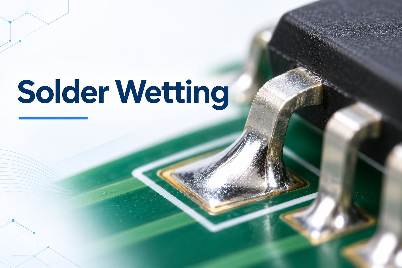
Solder wetting plays a critical role in PCB assembly by ensuring molten solder forms strong electrical and mechanical connections between PCB pads and component terminals. Poor wetting can lead to weak joints, incomplete solder coverage, and unreliable connections. This guide explains how solder wetting works, what causes common defects, and how to test, prevent, and resolve wetting problems.
At EBest Circuit (Best Technology), we support consistent solder wetting through free DFM reviews, controlled solder paste printing, nitrogen reflow, and SPI/AOI inspection. With four SMT production lines, 01005 component capability, and MES traceability, we provide reliable PCB assembly services from prototypes to mass production. Send your Gerber files, BOM, and quantity to sales@bestpcbs.com for a free DFM review and PCBA quotation.
What Is Solder Wetting and Why Does It Matter?
Solder wetting describes how molten solder spreads over and adheres to a solderable metal surface. During PCB assembly, solder wets the PCB pad and component termination, forming intermetallic compounds (IMCs) at the interface that contribute to a metallurgical bond.
Good wetting supports:
- Electrical conductivity: Creates a continuous connection between components and PCB pads.
- Mechanical strength: Supports the structural integrity of solder joints.
- Joint consistency: Promotes suitable solder coverage and fillet formation.
- Product reliability: Reduces the risk of wetting-related connection failures.
For example, a chip resistor may appear correctly positioned after reflow, but incomplete wetting at one termination can compromise its electrical connection.
The quality of wetting depends mainly on surface condition, solder alloy, flux activity, and soldering temperature. These factors should be considered together during material selection and assembly process development.
How Does the Solder Wetting Process Work?
The solder wetting process involves cleaning the metal interface, melting the solder, spreading across the surface, and forming a metallurgical bond. During SMT reflow, these reactions occur as the assembly passes through a controlled temperature profile.
The process follows five main stages:
- Surface Preparation: PCB pads and component terminations provide suitable solderable surfaces. Surface finishes such as ENIG, OSP, immersion silver, and immersion tin help protect the underlying metal before assembly.
- Flux Activation: Flux removes or disrupts oxides and helps protect the metal surfaces during heating.
- Solder Melting: The solder alloy reaches its melting range. SAC305 lead-free solder melts around 217–220°C, while Sn63Pb37 melts at approximately 183°C.
- Wetting and Bonding: Molten solder spreads across the metal surfaces, forming intermetallic compounds at the interface.
- Cooling: The solder solidifies and forms the final joint.
For tin-based solder on copper, Cu₆Sn₅ is a common intermetallic compound. Controlled intermetallic formation supports bonding, while excessive growth can affect joint properties.
The final joint shape depends on pad geometry, component termination, solder volume, and thermal conditions.
What Is a Good Solder Wetting Angle?
The solder wetting angle, or contact angle, measures the angle between molten solder and the solid metal surface at their contact point. A smaller angle generally indicates better solder spreading.
| Wetting Angle | General Interpretation |
| 0° | Idealized complete wetting |
| Below 90° | Wetting |
| 90° | Boundary condition |
| Above 90° | Non-wetting |
These values describe general wetting behavior rather than universal PCB solder joint acceptance limits.
In actual PCB assembly, engineers also evaluate solder fillets, joint coverage, and component-specific acceptance requirements.
A properly wetted solder joint generally shows:
- Continuous solder coverage on the intended surfaces.
- Suitable solder fillet formation.
- Smooth transitions between solder and metal surfaces.
- No obvious exposed areas caused by incomplete wetting.
The expected appearance varies between chip resistors, gull-wing leads, and BGA packages. Therefore, joint acceptance should follow the applicable IPC standards and component requirements rather than a single contact angle value.
Non-Wetting vs. Dewetting Solder: What’s the Difference?
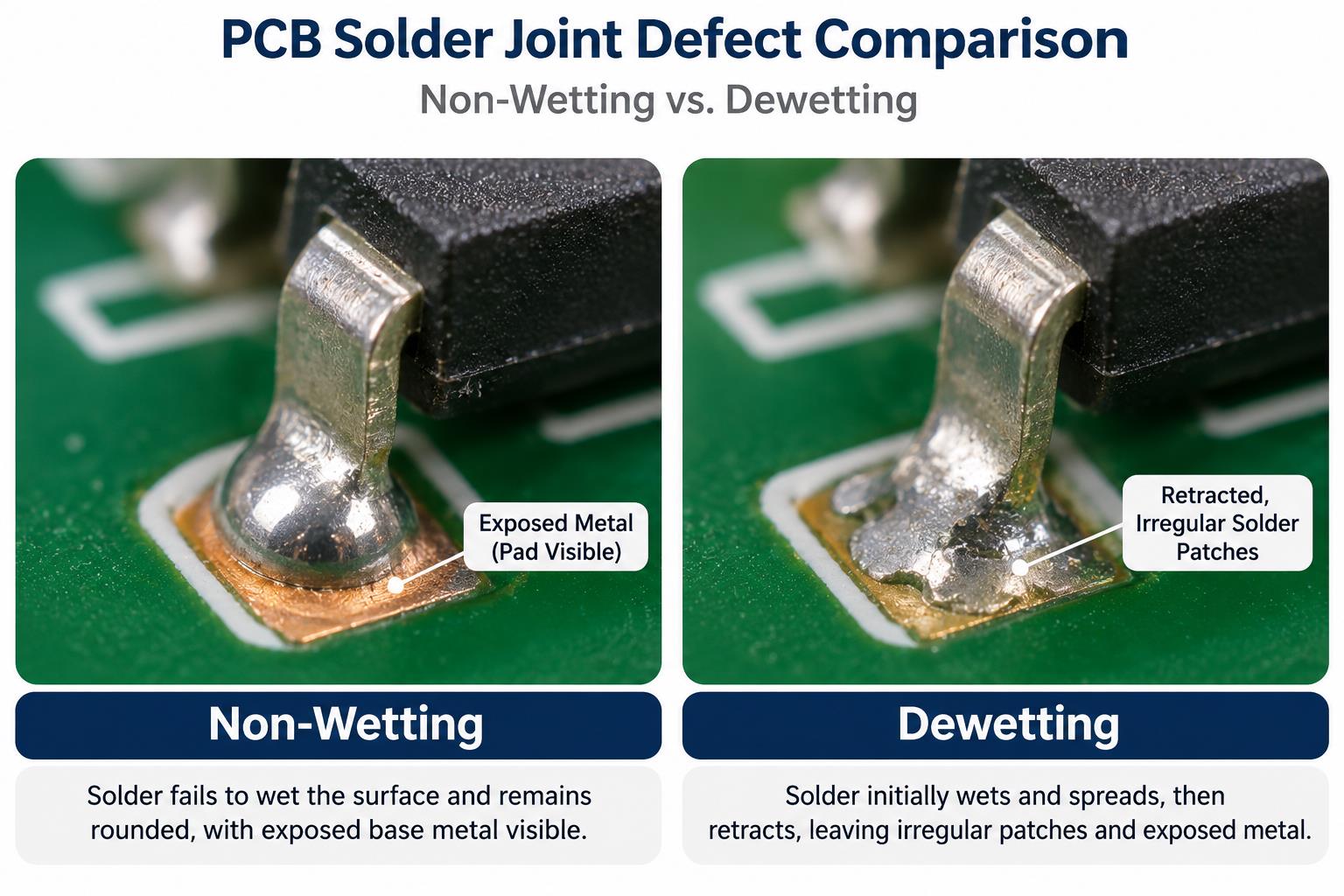
Non-wetting and dewetting are different soldering defects. Non-wetting occurs when molten solder fails to form an adherent coating on a metal surface. Dewetting occurs when solder initially wets the surface but later retracts, leaving exposed areas.
| Comparison | Non-Wetting | Dewetting |
| Initial behavior | Solder fails to wet | Solder initially wets |
| Appearance | Exposed metal, rounded solder | Irregular solder patches |
| Surface coverage | Incomplete from the start | Decreases after spreading |
| Common concerns | Oxidation, contamination, poor solderability | Oxidation, metallization, thermal exposure |
Non-Wetting: Molten solder may remain rounded instead of spreading across a PCB pad or component lead. Oxidized surfaces, unsuitable flux, and poor component solderability are common contributing factors.
Dewetting: Solder initially spreads but subsequently pulls away from portions of the surface. This can result from changes in surface condition, metallization problems, or unsuitable thermal exposure.
The distinction matters during troubleshooting. For non-wetting, engineers should first examine surface cleanliness and solderability. For dewetting, they should also investigate metallization quality and the soldering thermal profile.
What Causes Poor Solder Wetting in PCB Assembly?
Poor solder wetting usually results from oxidation, contamination, unsuitable solder materials, or incorrect thermal conditions. Identifying the actual cause is essential because increasing reflow temperature alone may not resolve the defect.
The following table summarizes common causes and their effects.
| Cause | Effect on Solder Wetting |
| PCB pad oxidation | Prevents proper solder spreading |
| Component terminal oxidation | Reduces termination solderability |
| Insufficient flux activity | Leaves surface oxides |
| Incorrect reflow profile | Disrupts melting and wetting |
| Unsuitable solder paste | Affects soldering performance |
| Surface contamination | Restricts metal-to-solder contact |
| Poor metallization | Creates an unsuitable solder interface |
PCB and Component Oxidation: Oxide layers interfere with the contact between molten solder and the metal surface. Proper packaging, controlled storage, and incoming inspection help maintain solderability.
Flux and Solder Paste Problems: Flux must provide sufficient activity for the selected surface finishes. Expired or improperly handled paste can affect printing and soldering performance.
Reflow Temperature: Insufficient heating may limit solder spreading, while excessive exposure can accelerate oxidation and intermetallic growth.
Surface Finish Problems: Coating defects, unsuitable metallization, and degraded surface finishes can also affect wetting.
When defects occur only on specific components or PCB batches, comparing the affected material with a known-good lot can help identify the source.
How Do Reflow Temperature and Solder Paste Affect Wetting?
Reflow temperature determines when solder melts and how long it remains liquid, while solder paste supplies the alloy and flux required for wetting. Both must work together to achieve consistent solder joint formation.
Reflow Temperature Control
| Reflow Stage | Function |
| Preheat | Gradually heats the PCB |
| Soak | Supports flux activity and thermal uniformity |
| Reflow | Melts solder and enables wetting |
| Cooling | Solidifies the solder joint |
Two important parameters are peak temperature and time above liquidus (TAL). Both should follow the solder paste manufacturer’s process recommendations and the thermal limits of the PCB and components.
For SAC305 solder, the melting range is approximately 217–220°C. The required peak temperature is higher than the melting range and depends on the approved process window.
Solder Paste Selection
The following factors influence soldering performance:
- Alloy composition: Determines melting characteristics.
- Flux activity: Supports oxide removal and solder spreading.
- Paste condition: Affects printing and process stability.
- Solder volume: Influences final joint geometry.
Nitrogen reflow can further support wetting by reducing oxidation during soldering. It is particularly useful for oxidation-sensitive assemblies and certain fine-pitch applications.
However, consistent results still depend on clean surfaces, compatible solder paste, and a properly developed reflow profile.
How to Prevent and Fix Solder Wetting Defects?
Preventing solder wetting defects requires suitable materials, controlled solder paste printing, and a validated reflow process. When a defect appears, engineers should identify its cause before applying corrective action.
Practical Troubleshooting Guide
| Defect | Check First | Corrective Action |
| Solder does not spread | PCB pad oxidation | Review surface finish |
| Solder beads on pad | Flux and surface condition | Verify flux compatibility |
| Solder retracts | Metallization and heating | Investigate dewetting |
| Poor wetting on leads | Component solderability | Check component lot |
| Uneven wetting | Reflow temperature | Measure thermal profile |
| Inconsistent joint formation | Paste printing | Review SPI results |
A reliable troubleshooting process follows five steps:
- Identify the defect: Examine solder coverage, joint shape, and affected component locations.
- Check the materials: Review PCB finishes, component terminals, solder paste, and storage conditions.
- Verify printing: Use SPI results to identify paste volume or alignment problems.
- Measure reflow conditions: Check peak temperature, time above liquidus, and temperature uniformity.
- Confirm corrective action: Reinspect the solder joints and compare results with the original defect.
For recurring issues, production records should include PCB lot numbers, component batches, solder paste details, and reflow profile information.
Rework considerations: Some wetting defects can be corrected through controlled rework. The joint condition, component temperature limits, and applicable acceptance criteria should determine whether rework or replacement is appropriate.
How Are Solder Wetting and Solderability Tested?
Solder wetting tests evaluate how molten solder spreads or interacts with a metal surface. Solderability tests determine whether PCB finishes and component terminations can form suitable solder connections under defined conditions.
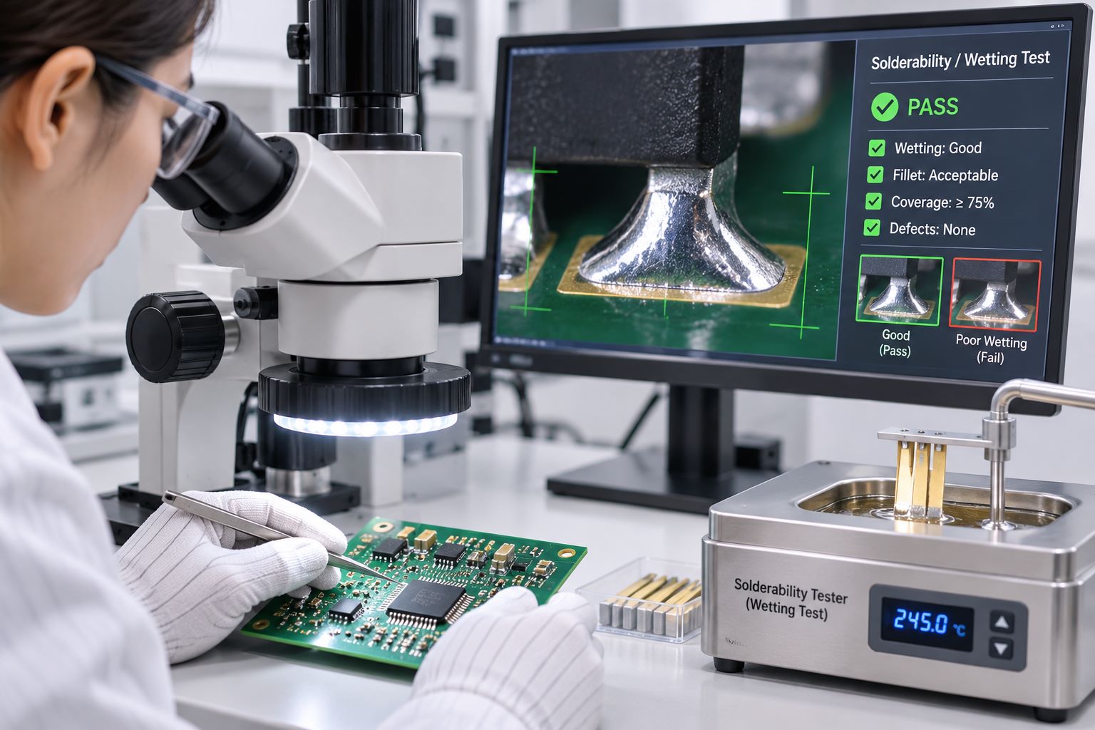
Different methods are used for incoming materials, assembled PCBs, and failure analysis.
| Test Method | Main Purpose |
| Wetting balance | Measures wetting force over time |
| Dip-and-look | Evaluates solder coverage |
| Contact angle test | Measures solder spreading |
| Visual inspection | Identifies visible wetting defects |
| AOI | Detects visible joint abnormalities |
| X-Ray | Examines hidden joint geometry |
| Cross-section | Evaluates internal solder interfaces |
Wetting Balance Test: Measures force changes as a specimen contacts molten solder. The resulting curve provides information about wetting behavior.
Dip-and-Look Test: Evaluates solder coverage after a component termination or other specimen is exposed to molten solder under controlled conditions.
AOI and X-Ray: AOI identifies visible assembly defects, while X-Ray examines hidden solder joint structures, including BGA connections. Neither method alone proves complete metallurgical wetting.
Relevant IPC Standards
- IPC-A-610: Electronic assembly acceptability.
- J-STD-001: Requirements for soldered electronic assemblies.
- J-STD-002: Component solderability testing.
- J-STD-003: Printed board solderability testing.
Solderability testing is particularly useful when materials have been stored for extended periods, a new supplier is introduced, or repeated wetting defects appear in a specific production batch.
How EBest Circuit Controls Solder Wetting Quality in PCBA
At EBest Circuit (Best Technology), solder wetting quality is supported by coordinated DFM review, solder paste inspection, nitrogen reflow, AOI, X-Ray, and MES production traceability.
With 20 years of electronics manufacturing experience, we combine PCB fabrication, component sourcing, PCB SMT assembly, inspection, and testing to support customers from prototypes to repeat production.
Our SMT Manufacturing Capabilities
| Capability | EBest Circuit |
| SMT production lines | 4: JUKI × 2, YAMAHA × 2 |
| Smallest SMT component | 01005 |
| BGA capability | 0.2 mm pitch |
| Reflow equipment | Nitrogen reflow |
| Solder paste inspection | 3D SPI |
| Joint inspection | AOI and X-Ray/AXI |
| Electrical testing | ICT and FCT |
| Traceability | MES, approximately 5-second retrieval |
| Minimum order quantity | No MOQ |
How We Control Soldering Quality
- Free DFM Review: Our engineers review pad geometry, component footprints, stencil considerations, and assembly risks before manufacturing.
- 3D SPI Inspection: Monitors solder paste deposits to identify printing abnormalities before reflow.
- Nitrogen Reflow: Helps reduce oxidation and supports consistent soldering conditions.
- AOI and X-Ray Inspection: Evaluate visible and hidden solder joint abnormalities using the appropriate inspection method.
- MES Traceability: Supports production record tracking and defect investigation at the individual PCB level.
- Engineering Support: One sales representative and three engineers coordinate technical questions, production requirements, and quality feedback.
Our quality management systems include ISO 9001, ISO 13485, IATF 16949, and AS9100D, supporting customer supplier qualification and controlled manufacturing requirements.
Need reliable PCB assembly with controlled soldering processes? EBest Circuit offers no-MOQ production, four SMT lines, nitrogen reflow, engineering support, and traceable quality control. Send your Gerber files, BOM, quantity, and target delivery date to sales@bestpcbs.com for a free DFM review, quotation, and production schedule confirmation.
FAQs About Solder Wetting
1. What Is the Difference Between Solder Wetting and Solderability?
Solder wetting describes how molten solder spreads across a metal surface. Solderability describes a material’s ability to form a suitable solder connection under specified conditions. Good solderability supports successful wetting during assembly.
2. What Is Insufficient Wetting in Soldering?
Insufficient wetting occurs when solder fails to spread adequately over the intended metal surface. Typical signs include exposed pads, incomplete solder coverage, and irregular solder fillets.
3. Does Lead-Free Solder Have Poorer Wetting Than Leaded Solder?
Some lead-free alloys have different wetting characteristics and higher melting temperatures than traditional tin-lead solder. Suitable flux, clean surfaces, and a controlled reflow profile help achieve reliable lead-free joints.
4. Can Poor Solder Wetting Cause PCB Failure?
Yes. Poor wetting can weaken electrical and mechanical connections, potentially causing intermittent faults or joint failures, particularly under thermal cycling or vibration.
5. Can Poor Solder Wetting Be Repaired?
Some defects can be corrected through controlled rework. Engineers should first identify the cause and evaluate pad and component condition. Damaged or severely oxidized surfaces may require replacement.
6. What Is the Best Way to Prevent Solder Wetting Problems?
Use solderable PCB finishes and components, compatible solder paste, controlled storage, verified stencil printing, and a suitable reflow profile. SPI, AOI, and traceability records help maintain consistent production quality.
Reliable solder joints start with the right materials, well-controlled soldering conditions, and effective inspection. EBest Circuit (Best Technology) combines 20 years of electronics manufacturing experience, four SMT lines, nitrogen reflow, SPI/AOI/X-Ray inspection, and MES traceability to help customers maintain consistent soldering quality. Backed by ISO 9001, ISO 13485, IATF 16949, and AS9100D certifications, we offer no-MOQ PCB assembly with engineering support from prototype validation to repeat production. Share your PCB design files, BOM, quantity, and delivery requirements with sales@bestpcbs.com for a manufacturing review, quotation, and lead-time confirmation.