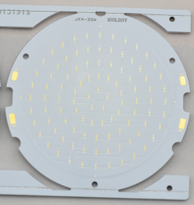
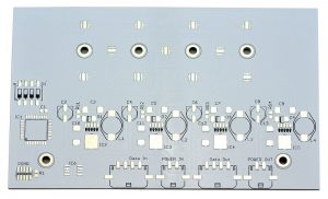
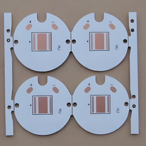
Two power assemblies can both show 15% projected solder voiding and still need different decisions. A single void beneath the main heat-transfer area can interrupt a larger share of that local path than several small voids near its edges. First confirm that both images used the same pad boundary. Then compare void location and size, and verify temperature under the same operating conditions. The percentage alone does not prove a thermal pass.
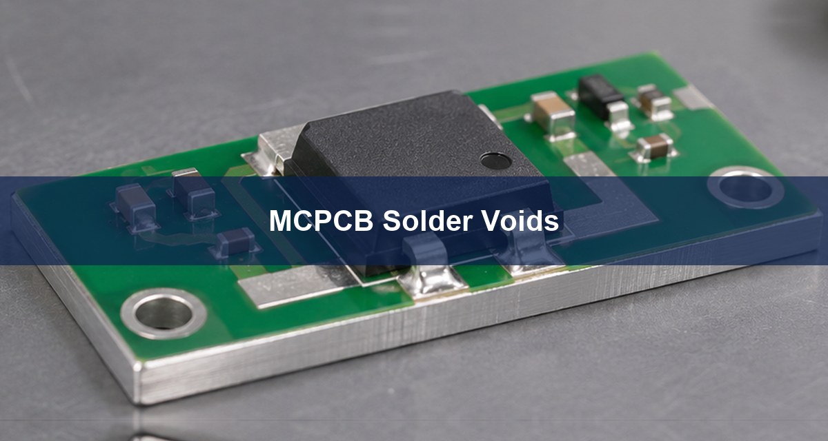
Metal Core PCB Stackup: Trace the Heat Path First
On a typical insulated metal substrate, heat flows from the package through its exposed pad and solder, then through the upper conductor and insulating dielectric into the metal base. The base may then transfer heat into a housing through a separate interface. A direct-thermal-path design can bypass the dielectric locally, but it still depends on the solder joint where the component meets the board.
In the motor-controller example below, assume the device is electrically and thermally connected at its exposed pad. Verify that requirement with the device drawing: depending on the part, the pad may be connected to ground, a power node or another specified potential. The metal base must not be treated as that net unless the approved construction makes the connection intentional. The thermal pad MCPCB guide explains those stackup choices.
Exposed Pad Soldering: Separate the Three Interfaces
The exposed package pad is not a soft thermal gap pad, and the solder underneath it is not the board-to-housing interface. A hot device can result from poor solder contact, the board dielectric, or uneven enclosure contact. Changing stencil openings will not fix an uneven heatsink fit. When troubleshooting, record device power and mounting conditions before comparing X-rays from two assemblies.
Use the exact package drawing and the supplier’s attachment guidance to define the required soldered region and net connection. Board copper outside the intended joint does not belong in the void calculation. An edge fillet or a good visual inspection does not establish coverage beneath the package.
Solder Void X Ray: Read the Projection
A top-down 2D X-ray combines attenuation along the beam. The inspection software can outline regions with less solder within a specified joint area. The resulting image is useful for screening, but does not locate a void in depth or prove that the two solder interfaces are fully wetted. Copper, features on the opposite side, and the metal base can change contrast.
Use the same orientation, magnification and segmentation settings when comparing units. Save the unannotated image plus the measured overlay. If bright spots track vias or repeat in features outside the pad, review the board data and image settings before counting them as voids. Document what the image could not separate rather than forcing a percentage for an unreadable region.
Solder Void Percentage: Use the Same Denominator
If the agreed evaluation region covers 20 mm² and the combined projected void area covers 3 mm², the total is 15%. Count overlapping projections only once in that total. It is an area fraction, not a volume fraction, and it cannot simply be multiplied by junction-to-ambient thermal resistance.
For a hypothetical central region of 6 mm², one 3 mm² void entirely inside it would cover 50% of that region. Six voids of 0.5 mm² outside the same region also give 15% overall but 0% inside the defined region. These assumed values show why the denominator and location matter; they are not factory data or acceptance criteria. Define a critical region using the package’s actual heat path or other approved evidence, not an arbitrary center circle.
| Finding | Unit A | Unit B |
|---|---|---|
| Total projected void area | 3 of 20 mm² (15%) | 3 of 20 mm² (15%) |
| Largest single void | 3 mm² | 0.5 mm² |
| Overlap with defined heat-transfer region | 3 of 6 mm² (50%) | 0 of 6 mm² (0%) |
| Next investigation | Verify central coverage and temperature margin. | Check edge wetting and confirm thermal performance. |
QFN Thermal Pad Voiding: Check the Actual Heat-Transfer Area
A large central void may be of greater concern if heat enters the pad mainly there. But an edge void can matter if it overlaps a critical portion of the electrical termination, disrupts solder wetting, or is subject to mechanical loading. The package drawing and thermal evidence, not the image center, determine which region deserves a separate evaluation. The Reliability Study of Bottom Terminated Components examines voiding and heat transfer on specific test assemblies. Its results are not a release limit for the devices in your build.
3D X Ray PCB Inspection: Know When to Escalate

Use an additional angled image if overlap obscures the pad outline or a nearby feature. If the depth of an indication changes the disposition, ask whether computed tomography can resolve it on this stackup; dense metal may limit usable contrast. A targeted destructive cross-section can verify the interface in the chosen plane, but cannot represent the entire joint on its own.
| Method | Best use | Limit |
|---|---|---|
| 2D X-ray | Compare projected area and distribution across units. | Overlapping features can mask depth or boundaries. |
| CT | Separate features through depth when resolution permits. | Metal and acquisition conditions affect visibility. |
| Cross-section | Inspect wetting, interfaces and thickness in a chosen slice. | Destructive and local, not a full-pad map. |
Solder Paste Stencil Design: Test One Change at a Time
Segmented apertures can change how paste deposits coalesce and how gases escape as solder melts. Do not infer the correct paste coverage from the final void percentage: printed paste and reflowed solder are different measurements. Start with the exact package guidance and verify the actual deposits with solder paste inspection before reflow.
When Unit A repeatedly shows a central void, compare the baseline against one proposed aperture layout with the same paste, package lot, profile and fixture. If the void does not respond, investigate wetting or the measured reflow profile rather than reducing paste until the X-ray looks better. Confirm that the change does not create opens or insufficient attachment at other joints. TI SLUA271C explains exposed-pad stencil considerations for QFN and SON.
Thermal Testing: Verify the Margin Before Release
Test representative assemblies at the specified worst-case operating point. Hold power, ambient temperature, heatsink contact, airflow and measurement method constant between samples. Use the package’s characterized temperature proxy or another approved junction-temperature method; the temperature of the aluminum base alone is not a junction measurement. If Unit A shows worse margin, verify the finding across more units before assigning causality. If both pass, still apply all agreed workmanship and electrical requirements.
A release record should include the PCB and stencil revisions, lot, pad evaluation boundary, total and largest void, location rule, image and thermal test record. IPC-7093A covers design and assembly considerations for bottom-termination components. Use the applicable purchase requirements and verified package guidance to define the inspection method and limits; do not adopt a blanket percentage from an unrelated package.
FAQ
Does 15% voiding always pass?
No. It is an example, not a threshold. Apply the written limits and check the measurement method.
Does more paste always reduce voiding?
No. Changing deposit coverage can change gas escape, component seating and other joints. Test a controlled change.
Is a hot QFN proof of poor solder coverage?
No. Check electrical dissipation and board-to-housing contact as well as the hidden joint.
Can a 2D image show where a void sits through the joint thickness?
Not by itself. A suitable additional view, CT or a cross-section can address the specific uncertainty.
Can I skip paste on a difficult center pad?
Only if the package documentation and approved design permit a different attachment. A ground or cooling function may depend on it.
Can I compare images from different inspection programs?
Only after verifying that the boundary, calibration and segmentation are equivalent for that joint.
Is a central void always worse than an edge void?
No. Risk depends on how heat, current and stress pass through the actual joint.
Does passing the thermal test clear an X-ray reject?
No. Treat thermal performance and agreed inspection criteria as separate release gates.
Discuss Your MCPCB Assembly Review
For a Best Technology review, send the package drawing, MCPCB stackup, pad and stencil files, sample X-rays and test conditions to sales@bestpcbs.com. Identify the heat path and the decision the inspection needs to support.