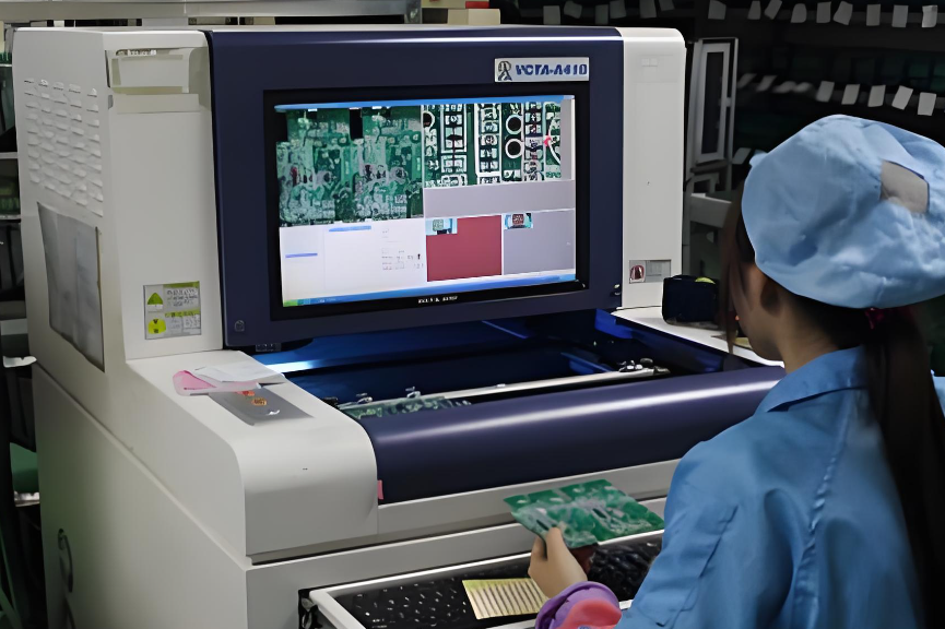
X-ray inspection is one of the most critical quality control methods in modern PCB assembly, especially for designs involving BGA, QFN, and high-density multilayer boards. As electronic products become smaller and more powerful, hidden defects such as voids, cracks, and insufficient solder joints are increasingly difficult to detect using traditional inspection methods.
In high-reliability industries like automotive, medical, and aerospace, these invisible defects are often the root cause of early product failure. This is why PCB X-ray inspection has become a standard process for manufacturers aiming to ensure long-term performance and minimize field returns.

What is X-Ray Inspection in PCB Manufacturing?
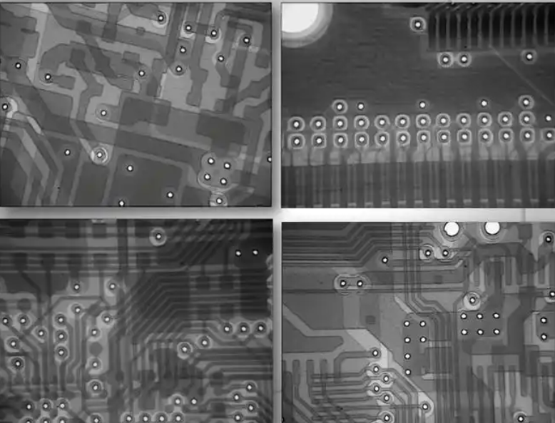
X-ray inspection is a non-destructive testing (NDT) technique used to analyze the internal structure of PCB assemblies without damaging them. It works by passing X-rays through the board and capturing differences in material density to generate a grayscale image.
In PCB assembly, X-ray inspection is commonly used to:
- Verify solder joint integrity under BGA and QFN packages
- Detect internal defects such as voids and cracks
- Analyze multilayer PCB structures and via quality
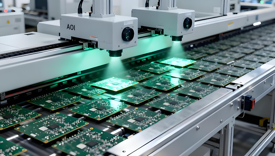
Compared to AOI, which only inspects visible surfaces, X-ray inspection for PCB assembly provides a complete internal view, making it essential for high-density designs.
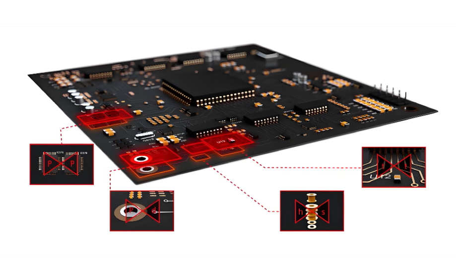
What Defects Can X-Ray Inspection Detect in PCBs?
X-ray inspection excels at detecting internal defects that are inaccessible to optical or electrical testing methods. These defects often originate from soldering issues, material inconsistencies, or process variations.
| Defect Type | Description | Impact |
| Solder Voids | Air gaps within solder joints | Reduced thermal and mechanical strength |
| Solder Bridges | Unintended connections between pads | Short circuits |
| Insufficient Solder | Incomplete joint formation | Weak electrical connection |
| Missing Solder | No connection at joint | Open circuit |
| Head-in-Pillow (HIP) | Poor wetting between ball and pad | Intermittent failure |
| Misalignment | Offset components or balls | Reliability issues |
| Internal Cracks | Structural defects in joints | Long-term failure |
| Via Defects | Barrel cracks or voids | Signal and power integrity issues |
Among these, voids in BGA solder joints are one of the most critical concerns. Excessive voiding reduces effective thermal conduction, leading to localized overheating. This is particularly problematic in high-power designs such as LED drivers or automotive control modules.
Which Components Usually Require X-Ray Inspection?
Not all components require X-ray inspection. It is typically used for packages with hidden or partially hidden solder joints.
Common Components Requiring X-Ray Inspection
- BGA (Ball Grid Array)
- Micro BGA
- QFN (Quad Flat No-Lead)
- LGA (Land Grid Array)
- CSP (Chip Scale Package)
- Flip-chip devices
These components are widely used in high-performance electronics. Their solder joints are located underneath the package, making external inspection ineffective. For these cases, X-ray inspection is the only reliable way to validate solder joint integrity.
When Should You Use X-Ray Inspection Instead of AOI?
AOI (Automated Optical Inspection) is widely used due to its speed and cost-effectiveness, but it is inherently limited to surface-level analysis. X-ray inspection in PCB assembly complements AOI by providing internal visibility.
Inspection Method Comparison
| Parameter | AOI | X-ray | ICT |
| Inspection Type | Visual | Internal | Electrical |
| Defect Coverage | Surface defects | Hidden defects | Functional issues |
| Cost | Low | Medium | High |
| Speed | Fast | Moderate | Slow |
| Typical Use | Placement, polarity | BGA/QFN inspection | Circuit validation |
In practice, X-ray inspection should be used when:
- The design includes hidden solder joints (BGA, QFN, LGA)
- The product requires high reliability (automotive, medical)
- There is a history of intermittent failures
- AOI results are inconclusive
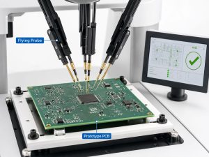
How Does X-ray Inspection Work in PCB Assembly?
The X-ray inspection system consists of an X-ray source, a detector, and an imaging system. The PCB is placed between the source and detector, and radiation passes through the assembly.
Key technical mechanisms include:
- Differential absorption: Materials with higher atomic numbers absorb more X-rays
- Magnification control: Enables micro-scale inspection of solder joints
- Digital image processing: Converts signals into high-resolution images
Advanced systems also incorporate:
- Automated defect recognition (ADR)
- Real-time measurement tools
- Image comparison algorithms
What Are the Main Types of X-Ray Inspection Systems?
Different applications require different levels of inspection capability. X-ray systems are generally categorized into several types.
Types of X-Ray Systems
| Type | Description | Application |
| 2D X-Ray | Flat image inspection | General inspection |
| 2.5D X-Ray | Angled views | Improved defect visibility |
| 3D CT (Computed Tomography) | Layer-by-layer imaging | Advanced failure analysis |
| AXI (Automated X-Ray Inspection) | Automated inline inspection | High-volume production |
In conclusion:
- 2D systems are cost-effective and widely used
- 3D CT systems provide the highest accuracy but are slower and more expensive
- AXI systems are ideal for automated production lines
What is the Difference Between 2D X-Ray and 3D CT Inspection?
Choosing the right X-ray technology depends on inspection objectives and budget considerations.
2D vs 3D CT Comparison
| Feature | 2D X-ray | 3D CT |
| Imaging Type | Projection | Volumetric |
| Inspection Speed | Fast | Slow |
| Cost | Lower | Higher |
| Defect Detection | General | Detailed internal |
| Application | Production line | Failure analysis |
2D X-ray is commonly used for inline inspection due to its speed and efficiency. In contrast, 3D CT provides cross-sectional views, enabling detailed analysis of complex defects such as internal cracks or multilayer misalignment.
How Much Does X-Ray Inspection Cost in PCB Manufacturing?
Cost is a critical consideration, especially for high-volume production. X-ray inspection pricing varies depending on inspection complexity, equipment type, and throughput requirements.
Typical Cost Breakdown
| Production Stage | Cost per Board | Notes |
| Prototype | $5–$20 | Manual inspection, low volume |
| Small batch | $2–$8 | Semi-automated |
| Mass production | <$1 | Inline automated systems |
Although it introduces additional cost, X-ray inspection significantly reduces:
- Field failure rates
- Warranty claims
- Rework and scrap costs
What Standards Define Acceptable X-ray Inspection Results?
Industry standards play a crucial role in defining acceptable defect thresholds. The most commonly referenced standards include:
- IPC-A-610: Acceptability of electronic assemblies
- IPC-7095: Design and assembly process for BGAs
Typical Acceptance Criteria Example
| Application Class | Void Limit | Reliability Requirement |
| Class 1 | Up to 30% | Consumer electronics |
| Class 2 | <25% | Industrial |
| Class 3 | <20% | Aerospace, medical |
What Are the Limitations of X-Ray Inspection?
Despite its advantages, X-ray inspection is not a complete solution. Understanding its limitations is essential for building an effective inspection strategy.
Key limitations include:
- Limited detection of surface contamination
- Overlapping structures in dense assemblies
- Requirement for skilled interpretation
- Higher equipment investment
For optimal results, X-ray inspection should be combined with AOI, ICT, and functional testing.
How to Interpret X-Ray Inspection Images Correctly?
Accurate interpretation is critical for effective defect detection. Engineers typically evaluate:
- Void distribution and percentage
- Solder joint symmetry
- Presence of cracks or gaps
- Alignment of components
Consistency is achieved through:
- Reference images
- Standardized criteria
- Software-assisted analysis
Misinterpretation can lead to false positives or missed defects, so training and experience are essential.
FAQs About X-Ray Inspection
1. What is X-ray inspection used for in PCB assembly?
X-ray inspection in PCB assembly is used to detect hidden internal defects that cannot be seen by visual inspection or AOI. It is commonly used to check solder joints under BGA, QFN, LGA, and other bottom-terminated components. It also helps verify solder quality, voiding, bridging, and internal connection integrity before products move to shipment or reliability testing.
2. Can X-ray inspection detect BGA defects?
Yes, X-ray inspection can detect BGA defects accurately because BGA solder joints are hidden beneath the component body. It is widely used to find solder voids, bridges, missing balls, insufficient solder, head-in-pillow defects, and ball misalignment. For BGA assembly, X-ray inspection is one of the most reliable quality control methods.
3. What defects can X-ray inspection find that AOI cannot?
X-ray inspection can find hidden solder defects that AOI cannot see. These include internal voids, solder bridging under bottom-terminated packages, missing solder joints, incomplete wetting, and internal cracks in some assemblies. AOI is useful for visible surface defects, while X-ray inspection is necessary for hidden joint analysis.
4. Is X-ray inspection destructive?
No, X-ray inspection is a non-destructive inspection method. It allows engineers to inspect the inside of a PCB assembly without cutting, breaking, or damaging the board. This makes it suitable for prototype verification, production inspection, and failure analysis.
5. When should 3D CT X-ray inspection be used?
3D CT X-ray inspection should be used when a standard 2D X-ray image does not provide enough detail. It is useful for complex assemblies, multilayer structures, internal failure analysis, and precise root-cause investigation. Compared with 2D X-ray, 3D CT gives a clearer view of internal structures layer by layer.
6. Is X-ray inspection required for every PCB assembly?
No, X-ray inspection is not required for every PCB assembly. It is usually recommended for boards with hidden solder joints, high-density packaging, high-power devices, or strict reliability requirements. For simple boards with fully visible joints, AOI and visual inspection may be enough.