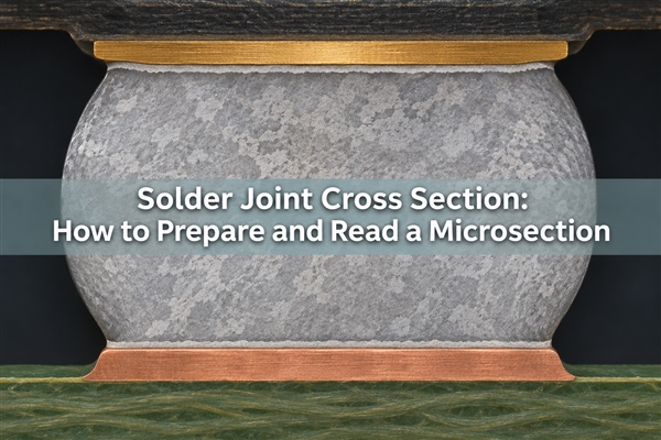
A solder joint cross section is a cut and polished view through a solder connection. It exposes the solder, component termination, PCB pad, and their interfaces in one plane. Engineers use it to investigate cracks, voids, incomplete wetting, or a suspected assembly failure that cannot be resolved from the outside. The section is destructive and represents only the plane that was prepared, so the sampling location and polishing quality matter as much as the image itself.
What Does a Solder Joint Cross Section Show?
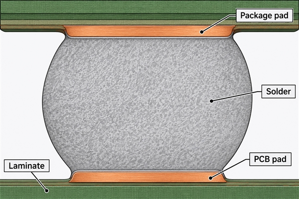
A cross section reveals the internal geometry of one chosen cut plane: the package-side pad, solder body, board-side land, and the interfaces where they meet. In an appropriate section, an analyst can see whether the solder contacts the intended metallized surfaces, where a discontinuity sits, and whether a crack follows an interface or crosses the solder.
The view is not a complete 3D map. A void that misses the cut plane may be invisible, and a slightly off-center cut can make a sound BGA ball look narrower than it really is. Record the package position, joint identifier, cut orientation, and whether the plane passed through the expected center before drawing a conclusion about geometry.
When Is Cross-Sectioning Worth the Destructive Test?
Use a microsection when the unresolved question concerns an internal interface, crack path, solder fill, or local microstructure, and a destroyed sample is acceptable. A common sequence is to document the failed unit, examine it visually, use non-destructive imaging if appropriate, and then cut the location most likely to answer the question.
It is a poor first step when only one field-return board exists and electrical mapping or X-ray could still localize the fault without damage. Preserve an uncut comparison joint or a good unit when available. Compare like packages, pad finishes, reflow histories, and locations; an isolated abnormal-looking plane is not automatically the root cause.
For example, if a BGA net fails only when the board flexes, first record the failing net and image the matching ball locations. If one corner ball shows a suspicious interface but the remaining sample is needed for electrical tests, keep it intact until those tests are complete. Section a matched failed unit or control build only when the question has narrowed to the local interface.
How Do You Choose the Joint and Cutting Plane?
Choose the joint that corresponds to the measured failure, not merely the easiest ball to reach. For a BGA corner failure, identify the ball row and side on board photographs or X-ray before removal. A planned cut through the ball center is useful for assessing overall shape and both pad interfaces, while a different plane may be needed to trace a localized crack.
Mark the package orientation and keep a cut map with the polished image. A section that grazes the side of a ball can understate its apparent width and miss the suspected pad edge; state which plane was actually reached, not just the one marked. IPC-TM-650 2.1.1 notes that some evaluations need more than one microsection. If the indication is three-dimensional, a second plane or an X-ray view may show whether the first section simply missed it.
How Is a Solder Joint Microsection Prepared?
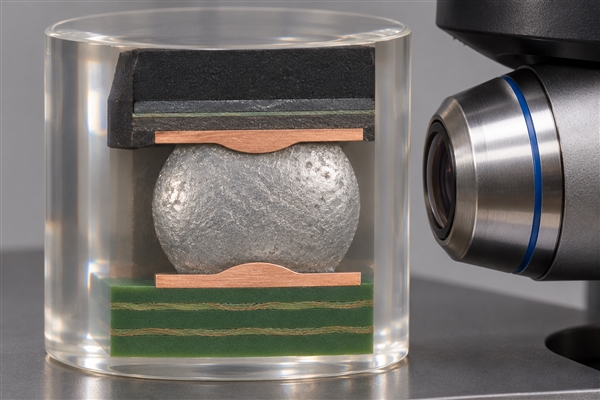
The basic sequence is select, remove, mount, grind, polish, and inspect. Remove the target area with enough clearance that cutting damage does not reach the joint. Mount the sample so the target plane remains stable during grinding, then approach it gradually under low-magnification checks rather than removing material in one pass.
Final polishing must preserve the solder-to-pad boundary. Smearing soft solder over a gap can hide a discontinuity; aggressive grinding can open a false separation. The IPC method describes manual and semi-automatic routes and emphasizes that technique and operator skill affect the result. Record the abrasive sequence and any etch or cleaning step so another reviewer can interpret the surface.
| Stage | Evidence to retain | What could mislead the reading |
|---|---|---|
| Selection | Board location, package orientation, failed-net map | Cutting a neighboring good joint |
| Mounting | Sample ID and intended section plane | Tilting the joint away from its center |
| Grinding | Approach photos or notes | Grinding past the feature of interest |
| Polishing | Final unetched and, if used, etched image | Solder smear or pullout resembling a defect |
The cut map and intermediate images let a reviewer tell where material was removed and whether a gap appeared during preparation. Choose abrasive media and equipment for the alloy, pad finish, and mount; a single final micrograph without that record cannot reliably distinguish a local defect from a missed or damaged plane.
Stop grinding while the target feature is still visible ahead of the polished face, then approach it in smaller passes. If the suspect ball disappears before its center is reached, record the overshoot and prepare another specimen rather than labeling the remaining edge view as a centered section.
How Do You Read Wetting and the Pad Interfaces?
Start at both metal interfaces. Look for continuous contact where solder should have wetted the package termination and the PCB land, then follow any interruption along its full visible length. A clear interface in the polished plane does not prove every part of the circumference is sound, but a genuine separation at the electrical path deserves further investigation.
Interpret the boundary with the pad finish and alloy in mind. Intermetallic material is part of a metallurgical solder bond; its mere presence is not a defect. Thickness, morphology, and significance require the actual alloy, thermal history, imaging method, and an applicable acceptance or reliability criterion.
When a dark line appears along a pad, compare its continuity and location with an intact joint from the same build. A polishing scratch that crosses solder and mount differently from the metal interface is not the same observation as a separation that follows the wetted boundary. If the distinction remains unclear, document it as unresolved and prepare another plane.
What Can Voids and Cracks Tell You?
A void is an empty region within a joint; a crack is a separation with a path that may cross solder, follow an interface, or connect to a pad edge. Their location often matters more than their appearance in one image. A small isolated void may have a different reliability effect from a void interrupting the load-bearing or current path, while a connected interface crack can explain an intermittent connection.
Do not label every cavity a failure. Compare the same package position with X-ray and any relevant electrical or thermal history, then apply the agreed product specification. Cross-sectioning can show the local relation between a void, crack, and pad, but a single 2D slice cannot establish total void volume.
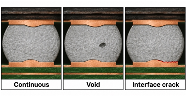
In the three illustrated joint states, the center cavity remains inside the solder while the right-hand separation reaches the lower pad interface. That difference changes the follow-up: map a suspected internal void across nearby joints with X-ray or CT, but trace a suspected interface crack against the failed net, board loading, and a comparable sound joint. The drawings show the location to inspect, not a pass/fail limit.
How Can Preparation Artifacts Mimic a Solder Defect?
Mechanical preparation can create a gap, pull out a brittle feature, or smear soft solder into an existing opening. An apparent crack that appears only after a rough polishing pass, lacks a coherent path, or runs along a damaged mount edge should be treated as provisional rather than automatically classified as an in-service fracture.
For a suspected pad-side crack, retain intermediate images and compare the as-cut surface, polished surface, nearby intact joints in the same mount, and any pre-cut X-ray at the same joint ID. If the opening appears or widens only after polishing, check for edge pullout or solder smear before assigning a service failure. Preserve both the observation and its alternative explanation; prepare another plane when the distinction changes the disposition.
Cross Section vs X-Ray Inspection: Which Answers the Question?
X-ray inspection is non-destructive and can map hidden BGA joint features across a board. A cross section sacrifices one location to expose the actual cut surface, interface, and local crack morphology. They answer different questions: X-ray is useful for locating a suspect area and observing volumetric features, while a microsection can examine the material boundary at that chosen location.
Neither technique replaces a defined acceptance criterion or electrical diagnosis. If X-ray suggests a void but continuity is stable, section the location only when the remaining risk justifies destroying the sample. If a net fails intermittently and X-ray is inconclusive, a section through the suspected pad interface can be more informative than another external image.
| Question | X-ray | Cross section |
|---|---|---|
| Locate hidden BGA anomaly across many balls | Strong first-pass option | Slow and destructive for broad screening |
| Inspect one solder-to-pad interface directly | Limited by overlapping projection and resolution | Direct view in the prepared plane |
| Estimate 3D distribution of internal voids | CT can help, subject to resolution | One 2D plane only |
| Preserve the failed unit | Yes | No |
For a failed BGA, the efficient order is usually electrical localization, non-destructive imaging, then targeted sectioning if the interface question remains. The comparison is about information gained and sample cost, not a claim that one method is always superior.
If the decision is whether several balls contain internal voids, one section cannot answer it because each cut samples only one plane. If the decision is whether a particular failed ball separated at its PCB pad, an X-ray projection may be inconclusive and a targeted section can provide the boundary detail. Choose the test from the remaining question, not from the availability of an instrument.
Which Dimensions and Test Conditions Belong in the Report?
A useful report gives measured geometry with its unit, plane, magnification or calibrated scale, and acceptance source. For example, if an optical image measures a 0.28 mm apparent solder width at the chosen plane, record that as a measurement of this plane, not the ball’s nominal diameter. Compare it with a same-location good joint or a drawing-defined target before inferring collapse.
IPC-TM-650 2.1.1 Rev F describes preparation, not a universal solder-joint width, void, or crack threshold. Its specimen-preparation guidance includes mounting material with a maximum cure temperature of 93 °C [200 °F]; that number concerns the mounting process, not a PCB operating limit or a solder acceptance limit. Use the applicable product drawing, assembly specification, and agreed test method for pass/fail decisions.
| Report field | Example entry | Interpretation boundary |
|---|---|---|
| Specimen and location | Board A, U7, ball C3 | Trace to failed net and cut map |
| Plane | Through intended ball center | Verify actual offset in the image |
| Measured width | 0.28 mm in this plane | Not a universal target or nominal ball size |
| Mounting material cure | At or below 93 °C per IPC method guidance | Preparation parameter, not joint acceptance |
| Disposition | Pending comparison with drawing and control joint | No invented pass/fail threshold |
The 0.28 mm width is a worked example of reporting format, not an observed result from our factory. The decisive step is pairing a calibrated measurement with the location and criterion. A number without those conditions is not an engineering verdict.
In an illustrative calibration, a 140-pixel span at 0.002 mm per pixel gives 0.28 mm in that image. The report must also say where the endpoints were placed and whether polishing reached the intended center. Without a drawing limit or matched control measurement, the calculation remains a documented dimension, not a pass/fail decision.
What Should a Failure-Analysis Report Include?
A failure-analysis report must let another engineer find the same joint and understand how its surface was produced. Record the electrical symptom and board ID first, then attach the location map and pre-cut evidence before presenting the micrograph.
- Identify the package, failed net, joint position, and actual section plane.
- Keep pre-cut photos or X-ray, mounting and polishing notes, and a calibrated image.
- State the observed feature, its measured location or extent, the acceptance source, and any unresolved alternative.
Separate observation from inference. “Separation visible along the lower pad interface in this plane” describes the image; “thermal cycling caused the failure” requires corroborating history and a comparison joint. Do not turn a visually striking but unconfirmed feature into a root cause.
Document the next action, not just the defect name. If a genuine interface separation is found, compare pad finish, paste deposition, reflow profile, handling, and mechanical support against a control build. If the section is ambiguous, say so and request a second plane rather than forcing a root-cause label.
How Can PCB and Assembly Design Reduce Repeat Failures?
Use the section result to isolate the process variable actually implicated. A pad-side issue may prompt review of land design and surface finish on the FR4 PCB; insufficient or inconsistent paste deposit may prompt review of the SMT stencil aperture and thickness. These are candidate checks, not conclusions that every crack or void originated in those steps.
For PCB assembly, we can coordinate board fabrication and assembly inputs so the failure review uses the right drawing, finish, paste, and package data. A second solder joint cross section from a control unit can then test the suspected difference. If you need a review, send the failed-net location, board drawing, package data, assembly process history, and desired quantity to EBest Circuit (Best Technology) at sales@bestpcbs.com; we can assess what evidence is available before proposing a destructive sample.