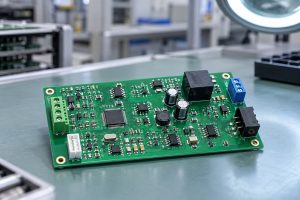
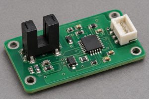
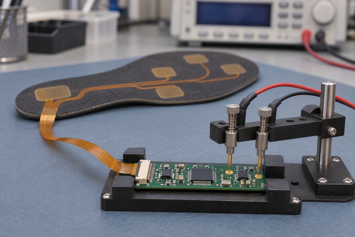
A smart insole combines sensors, signal processing, and power management inside a shoe insert to capture information about foot loading or movement. For product developers, the challenge extends beyond collecting data: the sensor connections must remain stable as the shoe bends, the electronics must fit without creating pressure points, and the assembled system must deliver repeatable readings. PCB construction and assembly therefore influence both physical integration and the quality of the signals available to the software.
EBest Circuit brings PCB fabrication, component sourcing, assembly, and testing into one coordinated service for wearable electronics. Our engineering team provides DFM review, BOM optimization recommendations, and process guidance to help resolve thin-board handling, connector fit, component placement, and test access before production. With support for prototypes and small batches, we help engineers move from a design revision to hardware they can evaluate. Email sales@bestpcbs.com, or visit Contact Us and complete the form at the bottom of the page to request a manufacturing review and quotation.
What Is a Smart Insole and How Does It Work?
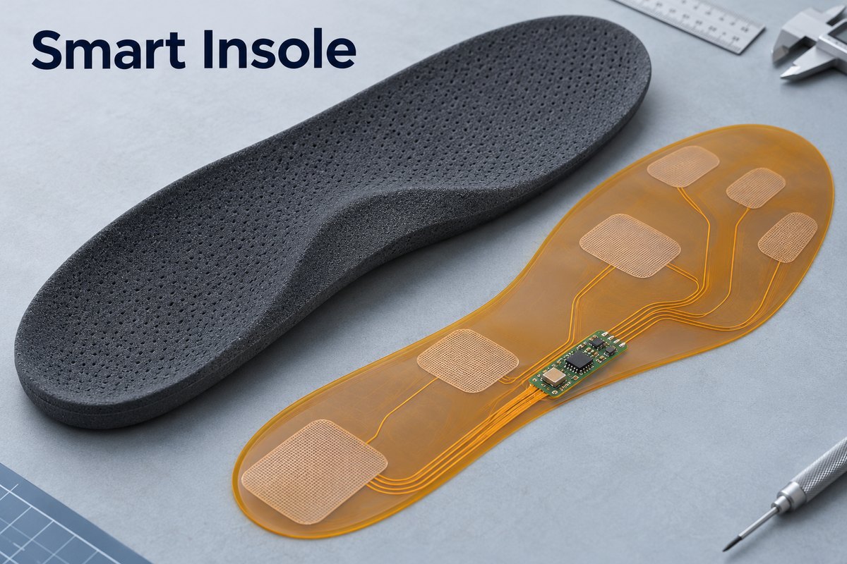
A smart insole is an electronic shoe insert that measures selected aspects of foot activity. Depending on its purpose, it may use pressure sensors, motion sensors, temperature sensors, or a combination of these devices. Not every model measures all three.
The basic operating sequence has four stages.
- Sensing. Pressure elements respond to loading, while an accelerometer and gyroscope capture motion. A temperature sensor adds thermal measurements when the application requires them.
- Signal acquisition. Analog circuitry and an analog-to-digital converter read analog sensors; digital sensors communicate through interfaces such as I²C or SPI.
- Processing and storage. A microcontroller organizes the readings, applies the configured processing, and may store samples locally.
- Communication. Bluetooth Low Energy can transfer data to a phone or receiver, where software displays trends, pressure distribution, or movement metrics.
PCB types used within the insole
Different parts of the system can use different board constructions.
- Flexible PCB (FPC). A flexible circuit can connect distributed sensing regions to the control electronics while following the insole’s shape. Repeatedly moving sections require a construction designed for dynamic bending.
- Rigid FR-4 PCB. A small rigid board can carry the microcontroller, wireless circuitry, and power-management components in a supported pocket. Multilayer construction provides additional routing space when component density requires it.
- Rigid-flex PCB. Rigid component sections and flexible interconnections form one circuit structure. This can reduce separate board-to-board connections, although its bend regions still need to match the mechanical movement.
- HDI or extra-thin PCB. HDI can help route compact, fine-pitch components; a thinner board can reduce the height of the electronics module. These features are selected when the design requires them, and a thin rigid PCB should not be treated as a repeatedly bendable FPC.
Running analysis, rehabilitation research, and foot monitoring use different combinations of these functions. A heated insole has a different primary task: controlling a heating element and its power safely. This article focuses on sensing electronics and their PCB assembly requirements.
How Do Pressure Sensing Insoles Measure Foot Pressure and Motion?
Pressure sensing insoles measure loading at selected positions beneath the foot. Motion measurement requires a separate sensing mechanism, commonly an inertial measurement unit, or IMU. Combining the two can associate changes in foot loading with movement during a step.
| Sensing approach | What it measures | Useful information | Main limitation |
|---|---|---|---|
| Piezoresistive pressure sensing | Resistance changes under applied load | Loading at individual sensing locations | Response can depend on loading history and calibration |
| Capacitive pressure sensing | Capacitance changes as the sensing structure deforms | Loading through a deformable sensor structure | Mechanical construction and parasitic capacitance affect the signal |
| Accelerometer and gyroscope | Acceleration and angular velocity | Motion patterns and orientation changes | Does not directly measure plantar pressure |
| Combined pressure and IMU sensing | Loading and motion on a shared timeline | Relationship between contact events and foot movement | Requires coordinated sampling and processing |
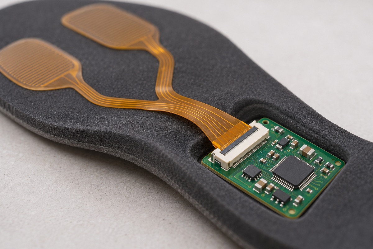
A pressure array needs electrical connections between its sensing regions and the acquisition electronics. Depending on the sensor technology, these connections may use a flexible printed circuit, printed conductors, or another interconnect structure. A flexible pressure sensor and an FPC are not automatically the same component.
The control board may contain the acquisition circuitry, microcontroller, wireless section, and power supply. Keeping sensor routing separate from noisy switching paths helps preserve the signals that later become a pressure map.
What Affects Insole Pressure Mapping Accuracy?
Insole pressure mapping accuracy depends on sensor response, mechanical integration, and data acquisition together. Adding more sensing points can improve spatial coverage, but it does not automatically make each measurement more accurate.
Sensor placement and coverage
The location and active area of each sensing element determine where loading is measured. A sparse array may identify broad loading patterns while missing a localized peak between elements. Software interpolation can make a display look smoother without adding measurements at those missing locations.
Calibration and loading behavior
Calibration relates sensor output to known loading conditions. Hysteresis means the response can differ between increasing and decreasing load; drift means the output can change over time under sustained conditions. Both matter when comparing measurements across a walking session.
The complete mechanical stack
Foam, adhesives, cover materials, and local rigid features affect how force reaches the sensing layer. A sensor calibrated by itself may behave differently after integration. Evaluation should therefore include the intended insole construction and representative loading.
Sampling, synchronization, and electrical noise
Sampling must capture the events the application needs to resolve. Left and right insoles also need suitable time alignment when their measurements are compared. Unstable supply rails, intermittent connections, or interference can introduce errors before the data reaches the analysis software.
At the assembly level, consistent connections and controlled component placement help preserve the design’s measurement potential. Final pressure accuracy still depends on calibration and validation of the complete sensing system.
How Do Sensor Insoles Withstand Repeated Bending and Sweat?
Sensor insoles need a mechanical layout that directs movement into suitable flexible regions and protects vulnerable electronics from moisture. A circuit that survives one installation fold is not necessarily suitable for repeated flexing during walking.
- Separate moving regions from component regions. Place rigid components, solder joints, and connectors where the mechanical design supports them. Avoid concentrating repeated bending at a connector exit or stiffener edge.
- Engineer the complete flex construction. Copper type, conductor geometry, layer count, coverlay, and total thickness all influence bending behavior. A thin circuit still needs a defined bend radius and motion profile.
- Relieve stress at transitions. The change from a flexible tail to a supported board can concentrate strain. Transition geometry and suitable strain relief help distribute that movement.
- Protect the right surfaces. Coating or encapsulation may protect control electronics, but contacts and sensing surfaces can require keepout areas. The protective material must also suit the intended movement.
- Evaluate the finished assembly. Flex cycling and moisture exposure should represent the intended use. Continuity and sensor response checks before and after exposure help reveal changes that a visual inspection can miss.
Sweat resistance depends on the housing, seams, materials, contacts, and electronics together. A coated PCB alone does not establish an ingress-protection rating for the finished insole.
EBest Circuit’s PCB Manufacturing and Assembly Capabilities for Smart Insoles
EBest Circuit supports rigid control boards, flexible interconnects, and rigid-flex constructions for wearable electronics. We connect fabrication decisions with component sourcing, assembly preparation, and inspection so that the sensor interface and control board can be reviewed as parts of the same build.
| Manufacturing item | Available capability | Application consideration |
|---|---|---|
| FR-4 layer count | 1–10 layers on the standard process route; high-Tg material required from 8 layers | Match routing needs to the available module thickness |
| FR-4 thickness with OSP or ENIG | 0.4–3.5 mm on the standard route | Applies to the rigid board, not the entire insole |
| All-flex construction | 1–4 layers and 0.06–0.60 mm finished thickness on one standard route | Final stackup must suit the bend and connection requirements |
| Inner-layer line width/spacing | 4/4 mil with 0.5 oz copper on the standard FR-4 route | Copper weight and geometry are evaluated together |
| Outer-layer line width/spacing | 4/4 mil with 1 oz copper on the standard FR-4 route | Relevant to compact component and connector routing |
| Minimum finished hole diameter | 0.20 mm standard; 0.15 mm through special processing | Subject to board thickness and hole construction |
| Assembly processes | SMT, through-hole, and mixed assembly | Selected according to the BOM and connection method |
| Inspection and functional testing | SPI, AOI, X-ray where applicable, and agreed functional tests | Coverage follows package type and the product test plan |
These are process options, not a single stackup that combines every limit. For a shoe insert, the flexible sensing area and rigid electronics section often need different constructions.
Our DFM review considers the connector contact geometry, flex-tail thickness, component support, panel handling, and access for programming or testing. The broader relationship between board construction and assembly is also covered in our wearable PCB guide.
For sensor-bearing assemblies, the manufacturing sequence must respect component temperature limits and any restrictions on cleaning, coating, or adhesive curing. These details help prevent a workable circuit design from becoming difficult to assemble consistently.
How Is an Insole Pressure Sensor Assembly Tested?
An insole pressure sensor assembly is tested in stages: first for manufacturing defects, then for electrical operation, and finally for the sensing behavior required by the product. Each stage answers a different question.
| Test stage | Typical checks | What the checks establish |
|---|---|---|
| Bare-board inspection | Netlist continuity, shorts, dimensions, and connector features | The fabricated circuit matches the electrical and mechanical requirements |
| Assembly inspection | Paste deposits, component orientation, visible solder joints, and applicable hidden joints | Placement and soldering meet the defined acceptance criteria |
| Electrical startup | Supply rails, startup current, programming, and communication | The board powers up and runs the intended test firmware |
| Sensor-channel checks | Channel identity, response to controlled inputs, open or inactive channels | Signals reach the correct acquisition channels |
| Wireless and power checks | Pairing, data transfer, sleep current, and charging behavior where fitted | Communication and power functions meet the agreed limits |
| Integrated product evaluation | Calibration, repeatability, flex exposure, and moisture-related checks | The finished construction performs under the specified conditions |
A useful functional test identifies the firmware revision and the operating state used for each measurement. For example, sleep-current results are only comparable when the radio, sensors, and processor are in the same defined state.
EBest Circuit can coordinate board inspection and project-defined functional testing with the build. Product-level calibration and environmental evaluation require their own fixtures, procedures, and acceptance limits; an AOI pass does not establish pressure accuracy or long-term wear performance.
Case Study in Smart Insole Electronics Assembly
A two-layer flexible sensor circuit from our manufacturing portfolio provides a relevant example for smart insole integration. This case focuses on the sensor interconnect and connector interface rather than a complete finished insole.
Application
The circuit uses a thin flexible construction to connect a sensing region to external electronics. In a smart insole architecture, this type of interconnect can link a sensing layer to a separately supported acquisition or wireless control board.
| Case parameter | Specified construction |
|---|---|
| Circuit type | Two-layer FPC |
| Finished FPC thickness | 0.13 ± 0.03 mm |
| Copper type | Rolled-annealed copper in an adhesive-based laminate |
| Coverlay | 0.5 mil coverlay film on one side |
| Surface finish | ENIG |
| Adhesive | 3M 467 |
| Connector interface | 1 mm pitch, 16 contacts |
| Sample build quantity | 6 sets, totaling 12 pieces |
Challenge
The manufacturing specification combined a thin flexible body with a revised connector contact pattern. The connector end needed controlled geometry, while the coverlay openings and adhesive arrangement had to remain consistent with the approved drawing. A change at this interface could affect how the sensor circuit connected to the next assembly.
Solution
The specified construction used rolled-annealed copper, a controlled FPC thickness, and ENIG on the exposed contact areas. The connector revision defined a 1 mm pitch and 16 contacts. Production artwork and a dimensioned PDF formed part of the customer approval process before manufacture, allowing the revised interface to be reviewed against the intended mating arrangement.
Customer Benefit
The thin circuit construction supports integration where space is limited, while a defined connector interface gives the electronics team a concrete basis for mating-board development. The small sample quantity supports fit and connection evaluation before a larger build. For smart insole development, the transferable value is early control of the sensor-to-controller connection, where thickness, contact geometry, and mechanical support must work together.
Why Choose EBest Circuit for Smart Insole PCB Assembly?
EBest Circuit combines engineering support with coordinated PCB and PCBA production. For a smart insole project, that means the flexible connection, compact control board, sourced components, and test requirements can be addressed through one manufacturing team.
- Engineering support that connects the sensor interface to the assembly process. Our team includes engineers with 20 years of PCB/PCBA experience. DFM review and BOM optimization recommendations help resolve connector compatibility, board handling, assembly access, and component availability while revisions are still practical.
- Quality systems relevant to controlled production. Our certifications include ISO 9001, ISO 13485, IATF 16949, and AS9100D. For health-monitoring electronics, ISO 13485 is particularly relevant to quality-system discussions. The applicable certification scope should match the contracted manufacturing service; these are company management-system certifications, not certifications of the finished insole.
- PCB fabrication and assembly under coordinated management. Our own PCB and PCBA factories, supported by more than 1,000 supply-chain partners, connect board production, procurement, assembly, and testing. This helps resolve questions that span the bare board, a purchased connector, and the final assembly without repeated supplier handoffs.
- Prototype and small-batch support. Engineers can evaluate connector fit, sensor interfaces, and programming access on an initial build before committing to repeat production. Manufacturing feedback can be incorporated into the next revision.
- Digital material and batch traceability. Traceability helps connect incoming materials and production batches with the build being evaluated. When a sensor, connector, or board revision changes, those records support investigation and repeat-order control.
These strengths are most useful when they are applied together: engineering review defines a practical build, sourcing keeps the approved components aligned with it, and production records preserve that definition through subsequent batches.
FAQs About Smart Insole Technology
Can a smart insole record data without a continuous phone connection?
Yes, if the hardware includes suitable memory and the firmware supports local recording. Storage capacity, sampling rate, and the upload method determine how long it can record before synchronization is needed.
Can one electronics design serve several shoe sizes?
A common control board may be reused, while the sensor layout and flexible interconnect change with the insole size. Channel mapping, tail routing, and mechanical fit still need to match each size.
Does a Bluetooth-enabled microcontroller always need a separate Bluetooth module?
No. Some microcontrollers integrate a Bluetooth radio. A separate module may simplify part of the RF implementation, but the choice depends on the design, antenna arrangement, firmware, and qualification strategy. It should not be added automatically as a duplicate function.
Can customers supply proprietary sensors for assembly?
Yes. Consigned or partial-turnkey assembly can accommodate customer-supplied parts. Handling instructions, packaging, temperature limits, and the agreed allowance for assembly are important for planning the build.
What determines the battery life of a smart insole?
Battery capacity, sensor excitation, sampling activity, radio transmission, processor operation, and sleep behavior all contribute. Battery life should be evaluated using the intended operating profile rather than inferred from the microcontroller’s lowest sleep-current figure.
What should happen when a sensor or connector becomes unavailable?
A substitute needs more than the same footprint. Electrical characteristics, pin assignment, mechanical fit, firmware compatibility, and calibration implications should be reviewed before approval. BOM review can identify alternatives early enough to reduce disruption to repeat builds.
Choose EBest Circuit for smart insole PCB assembly that connects practical engineering support with controlled manufacturing. Our ISO 9001 and ISO 13485 certifications, own PCB and PCBA factories, sourcing network, and digital batch traceability support the path from early samples to repeat production. You gain a team that can review the flexible interface and control board together, coordinate materials and assembly, and maintain clear production records as the design develops. Email sales@bestpcbs.com, or visit Contact Us, scroll to the bottom of the page, and complete the form to request a quotation and manufacturing review.