A silkscreen PCB uses printed text, symbols and outlines to guide assembly, inspection, testing and repair. The legend normally has no electrical function, but poor placement can hide polarity, confuse reference designators or leave critical text clipped during CAM preparation. A reliable design therefore controls character geometry, clearance, layer orientation and post-assembly visibility before the files reach fabrication.
The practical objective is not to place as much information as possible on the board. It is to preserve the markings that reduce manufacturing and service risk, while keeping every printed feature reproducible under the selected process. The following sections connect layout decisions with Gerber review, factory handling and finished-board acceptance.
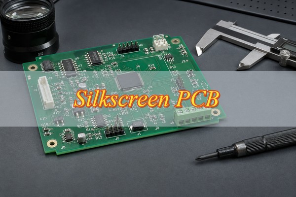
What Is Silkscreen PCB Marking, and Why Does It Matter?
PCB silkscreen identifies parts, orientation and product data. This nonconductive legend is commonly printed over the solder mask on one or both sides. CAD tools may call the layers Top Overlay and Bottom Overlay, while Gerber packages often use GTO and GBO.
The most valuable markings prevent a specific error. A visible Pin 1 symbol can stop an IC from being rotated, while clear polarity marks reduce the chance of reversed diodes or electrolytic capacitors. Connector names, test-point labels and revision codes also shorten inspection and troubleshooting because production teams do not have to reconstruct the design from the schematic.
- Assembly control: Reference designators, polarity and orientation marks support manual placement and line-side verification.
- Test access: Test-point names and interface labels help technicians connect fixtures and probes correctly.
- Serviceability: Readable identifiers reduce diagnostic time after the board has entered field use.
- Traceability: Board numbers, revisions, date codes and machine-readable marks connect the physical board with controlled records.
Silkscreen PCB vs. Solder Mask: What Is the Difference?
Solder mask protects copper; silkscreen communicates identification. Both appear on the outer surface, but they use separate design layers and serve different manufacturing purposes.
| Item | Silkscreen | Solder Mask |
| Purpose | Identification, assembly and service guidance | Copper protection and solderable-area control |
| Typical features | RefDes, polarity, labels, warnings, logos and revisions | Pad, via and other exposed-copper openings |
| Electrical role | None under normal use | Insulates and protects covered conductors |
| Common files | GTO/GBO or Top/Bottom Overlay | GTS/GBS or Top/Bottom Solder Mask |
| Placement rule | Keep clear of openings, edges and critical features | Open only where copper must remain exposed |
| Main risks | Clipped, blurred, hidden or misleading markings | Blocked pads, exposed copper or weak mask dams |
| Final inspection | Legibility, registration and content accuracy | Opening size, coverage, adhesion and defects |
Review silkscreen clearance against the actual mask openings, not copper pads alone. Solder mask expansion can make the opening larger than the pad and place nearby text inside the printing exclusion area.
What Information Should the PCB Silkscreen Layer Include?
Prioritize markings by the consequence of losing them. A silkscreen PCB layer should reserve space for safety, orientation and assembly information before branding or decorative artwork.
- Orientation: Pin 1, diode direction, LED polarity, electrolytic-capacitor polarity and connector direction.
- Component identity: Reference designators that match the BOM and assembly drawing.
- Interfaces: Connector names, terminal functions, switch positions and user-accessible controls.
- Test and service: Test-point IDs, fuse ratings, adjustment points and replaceable-module labels.
- Safety: High-voltage, hot-surface, ESD and other application-specific warnings.
- Product identity: Board number, product model, hardware revision and approved part number.
- Traceability: Date code, lot code, serial number, QR code or Data Matrix code.
- Compliance: Required certification or disposal marks whose use and minimum size have been verified.
- Branding: Company name and logo, retained only after functional markings have sufficient space.
When space is limited, retain safety, polarity, connector and test information first. Move secondary reference designators to the assembly drawing rather than shrinking them below a reliable size. Validate machine-readable codes using the intended scanner, lighting and working distance on the first article.
What Are the Minimum Silkscreen PCB Font Size, Line Width and Character Spacing?
Use production margin above the factory minimum. The current PCB capability data lists a general legend height and width of 28 × 5 mil, with a height-to-width ratio of at least 6:1. This is a manufacturing review reference, not permission to shrink every marking to that size.
| Feature | Design Check | Release Decision |
| Character height | Confirm text remains readable at the actual board scale | Use larger text for safety, polarity and manual inspection |
| Stroke width | Check narrow strokes, corners and enclosed spaces | Maintain production margin above the minimum |
| Character spacing | Look for merged letters and ambiguous numbers | Increase spacing or shorten the label |
| Reversed text | Review the narrow negative spaces around each character | Request engineering confirmation for fine reversed legends |
| Logo or code | Check the smallest line or module, not the total size | Validate the first article when scan performance matters |
Use a simple vector font with consistent strokes. Avoid compressed fonts, hairline artwork and tiny trademark details. Numbers such as 3, 5, 6, 8 and 9 deserve special attention because ink spread or a broken stroke can change their meaning. Special substrates, colors or unusually fine legends should be reviewed before the design is frozen.
How Much Clearance Should PCB Silkscreen Have From Pads, Vias and Board Edges?
Clearance protects both printability and meaning. For silkscreen PCB artwork, keep legends outside exposed pads, mask openings, test contacts, routed edges, slots and V-cut zones. Match the design rule to the selected factory’s registration capability rather than a generic online value.
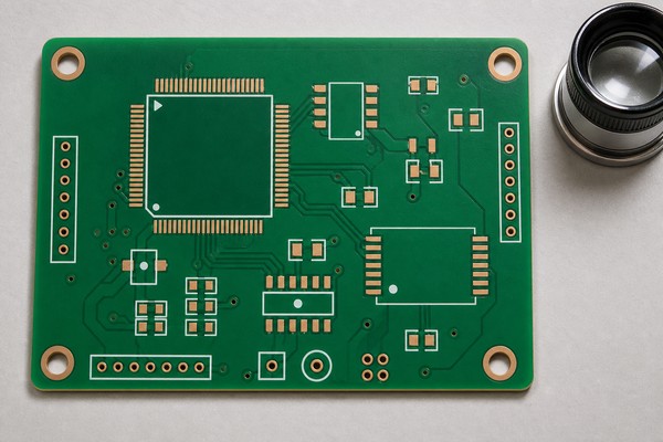
CAM software may clip silkscreen that enters a solderable opening. This protects the pad, but it can turn “R18” into “R1,” remove half of a polarity symbol or separate a warning from its icon. Do not assume the factory will move the remaining artwork, because automatic cleanup normally removes conflicts rather than redesigning the legend.
- Pad and mask clearance: Check the final mask opening and allow for registration variation.
- Via clearance: Distinguish tented vias from exposed test or thermal vias before applying a rule.
- Board-edge clearance: Keep critical text away from routing paths, slots, scoring and breakaway tabs.
- Component clearance: Use the assembly view or 3D model to confirm important markings remain visible after placement.
How Do Printing Method, Ink and Solder Mask Color Affect Readability?
Readability depends on the complete printing system. In a silkscreen PCB project, screen printing, liquid photo imaging and digital direct printing provide different resolution and setup options. Equipment, ink rheology, surface texture, curing and registration control can change the result from identical Gerber data.
Color contrast also affects inspection. Available silkscreen inks include white, black, red, orange, yellow, green, cyan, blue, purple and gray. Availability does not mean every color combination is equally readable. White legend over green or black mask often provides strong contrast, while similar-tone combinations should be checked on a physical sample.
The deeper PCB screen printing process is a separate manufacturing topic. Before design release, identify special colors, fine artwork, variable codes and adhesion-sensitive surfaces in the fabrication notes. This allows the factory to assess the process before production.
How to Check GTO and GBO Silkscreen Gerber Files Before Ordering
Gerber review must preserve the design intent. A silkscreen PCB check should use the exported files, not only the CAD view. Export settings, missing fonts, incorrect layer mapping or bottom-side orientation can alter the manufacturing package.
Step 1 — Confirm the layers. Verify that the required top and bottom overlay files are present and clearly identified. Do not rely only on file extensions because naming conventions vary between CAD systems.
Step 2 — Verify orientation. Inspect bottom-side text from the finished-board viewpoint. Confirm that mirroring is handled by the fabrication data and that readable text will not appear reversed on the manufactured board.
Step 3 — Overlay production data. View silkscreen together with solder mask, copper, drilling, slots and the board outline. Search for text over openings, symbols crossing routed features and artwork outside the finished profile.
Step 4 — Compare controlled documents. Match RefDes, Pin 1, polarity and connector names against the BOM and assembly drawing. Remove obsolete markings left behind after component changes.
Step 5 — Record exceptions. State color, side, special codes, critical warnings and any marking that must not be automatically clipped. Include a readable fabrication drawing when a requirement cannot be communicated reliably through Gerber data alone.
What Are the Most Common Silkscreen PCB DFM Errors?
Most failures begin with geometry or documentation errors. Finding them during DFM is less disruptive than discovering them at assembly inspection. Review each defect together with its production consequence and corrective action.
| Error | Consequence | Correction |
| Small text or narrow strokes | Broken, filled or unreadable characters | Increase geometry and simplify the font |
| Legend over a mask opening | Automatic clipping or ink near a solderable area | Move the item and rerun clearance checks |
| Incorrect bottom orientation | Mirrored text on the finished board | Verify GBO in an independent viewer |
| Outdated RefDes | Assembly and troubleshooting confusion | Reannotate and compare with the BOM |
| Hidden polarity symbol | Greater risk of reversed placement | Move the symbol outside the body outline |
| Artwork near the profile | Partial removal during routing or depanelization | Increase board-edge clearance |
If a delivered board has absent, blurred or shifted markings, use a structured PCB missing silk screen investigation. Separate source-file errors from CAM clipping, printing variation, surface condition and inspection criteria.
How Should Finished PCB Silkscreen Markings Be Inspected and Accepted?
Accept markings by legibility, accuracy and registration. Compare the result with approved fabrication data, and inspect safety and assembly-critical information more strictly than decorative artwork.
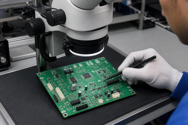
- Document match: Compare the finished board with the approved Gerber, fabrication drawing and assembly drawing.
- Content accuracy: Confirm board number, revision, RefDes, Pin 1, polarity, connector names and warning text.
- Completeness: Check that no required character, symbol, line or code is missing or unintentionally clipped.
- Legibility: Reject markings with broken strokes, filled characters, smearing, double images or ambiguous numbers.
- Registration: Verify that ink remains clear of pads, mask openings, exposed copper, slots and finished board edges.
- Post-assembly visibility: Confirm critical orientation, test and service markings remain visible after components are installed.
- Color and contrast: Compare the specified colors and confirm adequate contrast under normal inspection lighting.
- Adhesion: Use the agreed rub, tape or cleaning-resistance method when handling or field exposure may challenge the ink.
- Code verification: Scan each required QR or Data Matrix code with the intended device, distance and lighting.
- First-article record: Approve and retain the first-article result before releasing volume production when markings are critical.
Define critical acceptance criteria in the drawing or purchase specification. The phrase “clear silkscreen” alone does not establish allowable stroke loss, registration, color variation or scan performance.
What Silkscreen Requirements Should Be Confirmed When Ordering?
An RFQ must define content, placement and acceptance. For a silkscreen PCB order, send the final fabrication package rather than a preview image alone. This prevents avoidable clarification cycles.
- Manufacturing data: Supply Gerber or ODB++, NC drill data, board outline and fabrication drawing with matching revisions.
- Legend scope: State top, bottom or double-sided printing and identify non-negotiable safety or assembly marks.
- Appearance: Specify solder mask and silkscreen colors, including any approved sample or contrast requirement.
- Special artwork: Provide controlled vector data and verification rules for logos, serial numbers and machine-readable codes.
- Order context: Include quantity, prototype or production status, assembly requirements and first-article expectations.
- Change control: Require approval before critical text is clipped, moved or otherwise modified during CAM review.
Frequently Asked Questions About Silkscreen PCB Design
Q1: Can a circuit board operate without silkscreen?
A1: Yes, the bare circuit may still function electrically. However, removing the legend can increase assembly, test and maintenance risk. A design that relies on automated assembly and complete digital documentation may use fewer markings, but polarity, safety, connector and traceability information should be assessed before deletion.
Q2: Does silkscreen affect soldering?
A2: Correctly placed legend normally does not affect the solder joint. Problems arise when ink or artwork enters a pad, exposed-copper area or solder mask opening. The manufacturer may clip the conflict, but the remaining symbol can become misleading, so clearance should be corrected in the source design.
Q3: Can silkscreen be printed on both sides?
A3: Yes, double-sided silkscreen is available when both overlay files are supplied. Confirm the order calls for printing on both sides, review bottom orientation and check that bottom-side legends remain useful after the board is assembled into its enclosure.
Q4: What is the difference between GTO and GBO?
A4: GTO generally represents top overlay, while GBO represents bottom overlay. These names are common but not universal. Verify file content and layer mapping in a Gerber viewer instead of accepting an extension without inspection.
Q5: Should every component have a reference designator?
A5: Not necessarily, especially on dense layouts. Preserve identifiers that support assembly, inspection and service. Secondary RefDes can remain in the assembly drawing when board space is limited, provided the documentation is controlled and accessible to the production team.
Q6: Which silkscreen color is easiest to read?
A6: The best choice provides strong contrast with the solder mask. White is commonly readable on green, blue, red and black masks, but the result also depends on ink coverage and surface finish. Confirm unusual color combinations with a physical sample.
Q7: Why does a factory clip silkscreen around pads?
A7: Clipping prevents legend ink from entering exposed solderable areas. The operation protects manufacturability but may remove part of a label or polarity symbol. Correct the source placement and identify critical marks instead of relying on automatic cleanup.
Q8: Can a QR code be placed on the silkscreen layer?
A8: Yes, provided the printed module size and contrast support reliable scanning. Test the first article using the intended scanner, distance and lighting. For very small codes, discuss alternative marking processes before finalizing the layout.
Q9: Is the smallest printable text also the recommended text size?
A9: No; a manufacturing minimum is a limit, not an ideal production target. Larger characters and wider strokes improve process margin and field readability. Use the minimum only after considering inspection distance, substrate, ink, printing process and consequence of misreading.
Q10: What should be sent for a silkscreen DFM review?
A10: Send the complete, revision-matched fabrication package. Include Gerber or ODB++, NC drill data, fabrication and assembly drawings, BOM when assembly is involved, color requirements, critical markings and acceptance criteria for logos or codes.
Conclusion
Reliable silkscreen supports assembly, inspection and service. Control text geometry, preserve clearance from openings and profiles, verify both overlay files, and define which markings are critical. Procurement should confirm colors, sides, artwork and acceptance criteria before production.
For a silkscreen PCB review, send the Gerber or ODB++ package, NC drill files, fabrication and assembly drawings, quantity, colors and critical marking requirements. Contact our engineering team at sales@bestpcbs.com for DFM support and a manufacturing quotation.