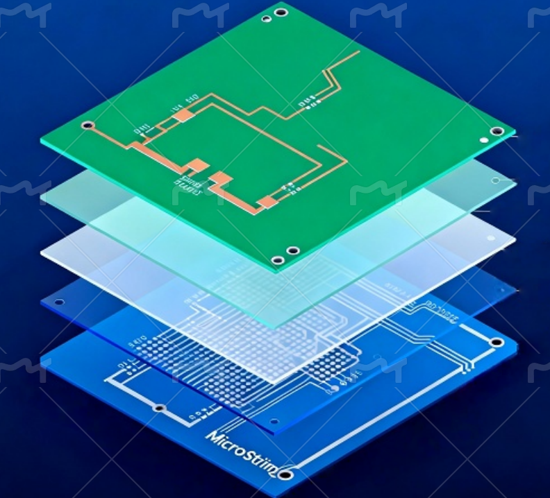
The relative permittivity of FR4 is commonly estimated at about 4.4. That estimate is useful during early layout, but the final Dk depends on the laminate system, glass-resin construction, frequency, test method, and modeling purpose. These distinctions affect controlled-impedance geometry, effective signal velocity, propagation delay, and phase, so a reliable PCB design separates reference Dk, measured datasheet Dk, Design Dk, and effective permittivity before trace geometry or timing limits are finalized.
What Does Relative Permittivity Mean in FR4?
Relative permittivity of FR4, written as εr and commonly called dielectric constant or Dk, is the ratio between the material’s permittivity and the permittivity of a vacuum. Because it is a ratio, Dk has no unit. A material with a higher Dk stores more electric-field energy than a material with a lower Dk under the same field conditions.
On a PCB, that stored field energy contributes to the capacitance per unit length of a trace. Capacitance and inductance together set the trace’s characteristic impedance and propagation velocity, which is why Dk appears in transmission-line and stackup calculations. Dk should not be confused with dissipation factor, or Df: Dk primarily influences impedance and phase velocity, while Df describes dielectric energy loss.
The laminate Dk is also different from the effective permittivity experienced by a finished trace. A microstrip shares its electric field between the laminate and air, while a stripline contains almost all of its field within dielectric. The same laminate can therefore produce different effective signal velocities on different layers.
What Is the Typical Relative Permittivity of FR4?
About 4.4 is the usual general-reference value for FR4. A preliminary range of approximately 4.0–4.4 is reasonable when the material and stackup have not yet been chosen, but neither value is precise enough to release controlled-impedance geometry. Once a laminate construction is selected, the model should use data that matches that construction, the intended frequency range, and the type of calculation.
| Design Stage | Dk Input |
|---|---|
| General reference | About 4.4 |
| Early estimate | About 4.0–4.4 |
| Selected laminate | Construction-specific data |
| Controlled impedance | Applicable Design Dk |
| Broadband or RF model | Frequency-dependent data |
These values belong to different levels of design certainty. The preliminary range can reserve routing space and expose an obviously impractical stackup. It cannot confirm final trace width because the actual glass style, pressed dielectric thickness, copper geometry, and modeling Dk remain unknown. The Dk input should become more specific as the electrical requirement becomes less tolerant of variation.
How Do Glass Weave and Resin Content Affect FR4 Permittivity?
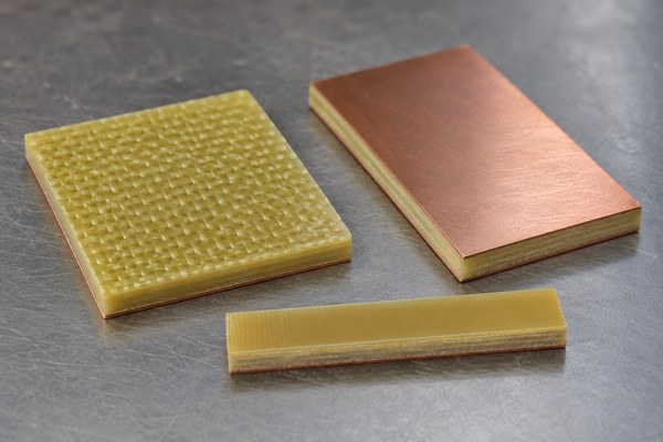
FR4 is a composite of glass reinforcement and cured resin, and the two constituents have different permittivity. Glass-rich constructions generally produce a higher composite Dk, while resin-rich constructions generally produce a lower value. Glass style also changes the distribution of resin and glass through the dielectric, so two cores from the same laminate family can require different Dk inputs.
The table compares published typical core data for two FR408HR constructions measured under the same reported frequency points.
| Construction | Resin | 100 MHz | 1 GHz | 10 GHz |
|---|---|---|---|---|
| 106 | 72% | 3.37 | 3.34 | 3.30 |
| 1080 | 57% | 3.67 | 3.62 | 3.59 |
At 1 GHz, the 1080 core is reported at 3.62 and the more resin-rich 106 core at 3.34, a difference of 0.28. That is about 8.4% relative to the 106 value and is large enough to change a controlled-impedance solution. These are typical core values for the stated constructions, not interchangeable values for every core or prepreg. Final impedance and delay models should identify both the laminate grade and the production construction.
Glass weave also creates small local changes in field environment. A narrow trace may run mainly over a resin-rich opening or closer to glass bundles, which can contribute to pair-to-pair skew in demanding high-speed designs. Routing angle, wider traces, spread-glass options, and tighter construction control can reduce that sensitivity when the available timing margin makes it relevant.
How Does Frequency Affect the Relative Permittivity of FR4?
FR4 is dispersive, so its reported Dk changes with frequency. In the FR408HR 106-core example, the published value is 3.37 at 100 MHz, 3.34 at 1 GHz, and 3.30 at 10 GHz. The decrease from 100 MHz to 10 GHz is approximately 2.1%.
A small percentage change can still matter over a long route or a narrow phase budget. It changes effective permittivity, shifts calculated impedance, and accumulates as propagation delay. A solver that accepts one Dk value should therefore use a value near the band that drives the electrical requirement. A broadband model may require a dispersive material model rather than one fixed point.
For digital channels, clock frequency is not the only frequency reference. Edge rate determines how much high-frequency spectral energy the interconnect must carry, while channel bandwidth and loss determine which part reaches the receiver. A low clock rate with fast edges can require material data at frequencies well above the clock fundamental. Rise time, channel bandwidth, and the required phase or delay accuracy provide a better basis for selecting the relevant Dk data.
How Do Test Methods Affect Reported FR4 Dk?
A Dk result is meaningful only with its test method, frequency, and specimen condition. Parallel-plate, clamped-stripline, resonator, and circuit-based methods create different field distributions and handle fixture and specimen effects differently. Values produced by different methods can therefore disagree even when both measurements are valid.
Specimen thickness, resin content, copper removal, surface condition, clamping pressure, and air gaps can influence the result. Material anisotropy adds another distinction: an in-plane transmission-line measurement does not necessarily represent the same dielectric direction as a through-thickness capacitance method. Comparing two numbers without these conditions can create a false material difference.
When two sources report different Dk values, compare the method, test frequency, construction, sample conditioning, and whether the value is a measured specification or a design recommendation. Values should be transferred into the same model only when those conditions and intended uses are compatible.
What Is the Difference Between Datasheet Dk, Design Dk, and Effective Permittivity?
Datasheet Dk describes a published material result, Design Dk is intended for transmission-line modeling, and effective permittivity belongs to a specific trace structure. Treating the three as synonyms is a common source of impedance and delay errors.
- Datasheet Dk: A value reported for a stated material, specimen, frequency, and test method. It supports material comparison only when the reported conditions are comparable.
- Design Dk: A laminate value selected or derived to improve correlation between transmission-line calculations and fabricated circuits. It is the preferred material input when the supplier provides it for the relevant product, construction, and frequency.
- Effective permittivity, εeff: The field-weighted value experienced by a particular microstrip, stripline, or coplanar structure. Geometry, layer location, solder mask, and the surrounding media all influence it.
For a microstrip, part of the field travels through air, so εeff is normally below the laminate’s bulk or Design Dk. A stripline is surrounded by dielectric and its εeff is usually closer to the laminate value. An effective microstrip value is not a valid laminate input when the field solver expects bulk or Design Dk. The material value goes into the model; the solver then calculates the structure’s effective behavior.
How Does FR4 Permittivity Affect PCB Impedance?
With geometry held constant, a higher Dk generally lowers characteristic impedance. Transmission-line impedance is related to the ratio of inductance to capacitance per unit length. A higher material permittivity increases electric-field storage and capacitance, reducing impedance unless the geometry changes.
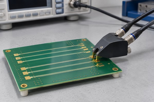
For a 50 Ω single-ended line, a Dk increase may require a narrower trace or greater distance to the reference plane. Differential impedance also responds to pair spacing because coupling changes the even- and odd-mode capacitance. Copper thickness, trapezoidal etch shape, solder mask, and finished dielectric thickness modify the result at the same time, so a Dk percentage change does not translate into an equal percentage change in impedance.
The practical check is a sensitivity run using the proposed production stackup. Calculate the nominal line, then repeat the model at the expected Dk and geometry limits. If the resulting impedance range exceeds the drawing tolerance, the design needs a different geometry, a tighter construction, or a more controlled laminate definition before routing is frozen.
How Does FR4 Permittivity Affect Signal Speed and Propagation Delay?
A higher effective permittivity reduces wave velocity and increases propagation delay. For a simplified nondispersive transmission line, v ≈ c / √εeff. The corresponding delay is approximately 84.7 ps/in × √εeff.
At εeff = 3.2, the estimated delay is about 151.5 ps/in. At εeff = 3.6, it is about 160.8 ps/in. Across a 10-inch route, the difference is approximately 93 ps. This comparison isolates the effect of εeff and is not a universal FR4 delay value.
Delay variation matters when it consumes setup-and-hold margin, pair skew, phase alignment, or a length-matching budget. Layer changes deserve particular attention: a microstrip and stripline can have different εeff even when they use the same laminate system. Matching copper length alone does not guarantee equal electrical delay when two routes see different constructions or field distributions.
For timing review, convert the modeled delay into ps/in for each relevant layer and compare the accumulated difference with the available budget. That check is more reliable than applying one generic propagation factor to every layer in the stackup.
Which FR4 Permittivity Value Should You Use for PCB Design?
The correct Dk input depends on the design stage and the decision being made. Early placement needs a plausible estimate; released impedance and timing constraints need construction-specific data.
- Preliminary PCB design: Use about 4.0–4.4 as a documented assumption while the material remains open. Model more than one value if routing space is tight, and avoid fixing the final trace width from this estimate.
- Selected laminate: Use data for the chosen product and glass-resin construction at the relevant frequency. Confirm whether the stated number is a test-method result or the supplier’s recommended modeling value.
- Controlled-impedance or high-speed PCB: Use the applicable Design Dk with the finished dielectric thickness, copper geometry, solder-mask condition, and a construction that can be supported in production.
A value of 4.4 is useful for early feasibility work, but it should not automatically become the released Dk for a controlled-impedance board. Before final routing, the laminate identity, construction, frequency basis, solver definition, and proposed stackup should describe the same physical build.
When Is a Generic FR4 Dk Value No Longer Accurate Enough?
A generic value stops being adequate when Dk uncertainty consumes a meaningful share of the electrical margin. The decision is set by the channel requirement, not by one universal frequency threshold.
- Impedance margin is narrow: Model the expected Dk and geometry limits. If the calculated range approaches or exceeds the impedance tolerance, use controlled construction data and agree on achievable finished dimensions.
- Delay, skew, or phase is tightly budgeted: Convert Dk uncertainty into delay across the actual route length and layer transitions. Construction-specific data is needed when that uncertainty is no longer small relative to the timing budget.
- The channel is broadband or loss-sensitive: Review Dk dispersion and Df over the band that reaches the receiver. A single low-frequency value cannot describe broadband phase and loss behavior.
- A laminate substitution is proposed: Compare construction, Design Dk, Df, and finished dielectric thickness, then recalculate impedance and delay. Matching Tg or nominal board thickness does not establish electrical equivalence.
When the modeled worst case leaves insufficient margin, the practical choices are tighter construction control, a laminate with better-characterized electrical data, a revised stackup, or more tolerant routing constraints. This connects material selection directly to the requirement that is at risk.
FAQs About FR4 Relative Permittivity
Q1: Is the relative permittivity of FR4 always 4.4?
A1: No. About 4.4 is a general estimate; actual values vary with laminate formulation, glass-resin construction, frequency, and test method.
Q2: Is relative permittivity the same as dielectric constant?
A2: Yes in PCB material discussions. Relative permittivity, dielectric constant, εr, and Dk commonly identify the same material property.
Q3: Does FR4 Dk change with frequency?
A3: Yes. FR4 is dispersive, so the modeling value should correspond to the relevant signal band.
Q4: Does PCB thickness affect FR4 permittivity?
A4: Board thickness does not directly redefine Dk, but achieving a different thickness can require another glass-resin construction with different electrical data.
Q5: What FR4 Dk should be used for a 50-ohm trace?
A5: Use the applicable Design Dk for the selected construction and solve it with the finished trace and stackup geometry.
Q6: Is effective permittivity the same as FR4 Dk?
A6: No. FR4 Dk is a laminate property; effective permittivity is the field-weighted result for a particular transmission-line structure.
Q7: Why do different FR4 datasheets show different Dk values?
A7: The products, constructions, frequencies, specimen conditions, test methods, or reporting purposes may differ.
Q8: Does FR4 permittivity affect signal propagation speed?
A8: Yes. Higher effective permittivity generally reduces wave velocity and increases propagation delay.
FR4 has no single Dk that fits every PCB calculation. About 4.4 is suitable for early estimates, while controlled-impedance, timing-sensitive, and broadband designs need a value tied to the selected laminate, glass-resin construction, relevant frequency, and modeling method. That distinction keeps the material data, stackup geometry, impedance target, and delay calculation consistent.
If your PCB requires controlled impedance, high-speed routing, or a tight delay budget, send the layer count, target impedance, preferred laminate if known, and key interface to sales@bestpcbs.com. BestPCBS can review the proposed stackup and Dk assumptions before the trace geometry is finalized.