Selective soldering in PCB assembly is a strong option when a mixed-technology board needs repeatable through-hole joints without exposing the entire underside to a solder wave. It is not automatically the best choice for every connector or production volume. The decision depends on joint count, nozzle access, nearby SMDs, thermal demand, cycle time, and the evidence required for production release.
EBest Circuit supports PCB fabrication, component sourcing, SMT, through-hole assembly, and manufacturing review within the agreed PCBA scope. If you want to compare selective soldering with wave or controlled hand soldering for a released board, send the PCB files, BOM, quantities, and acceptance requirements to sales@bestpcbs.com.
What Is Selective Soldering in PCB Assembly?
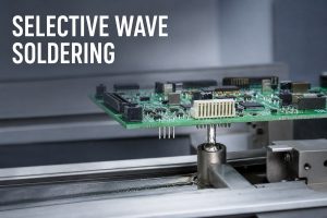
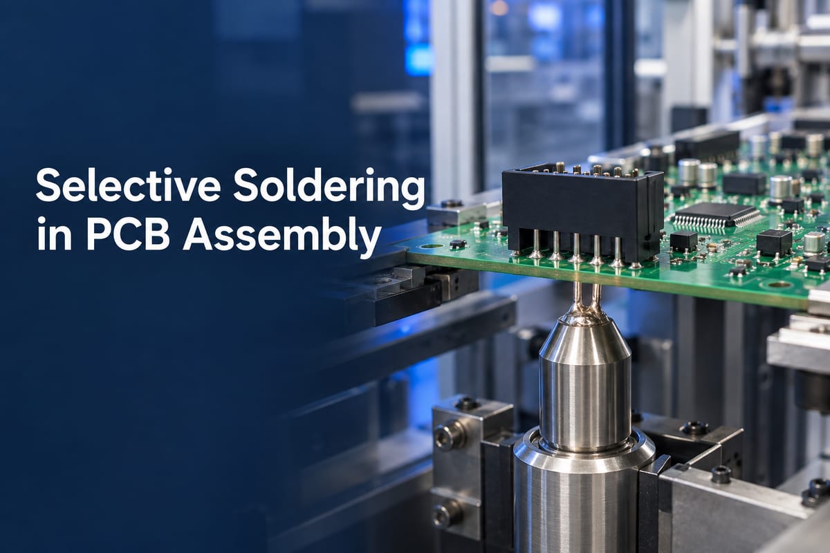
Selective soldering applies flux, heat, and solder only to chosen through-hole joints or joint groups. A programmed system moves the board or solder nozzle so that molten solder reaches the required pins while avoiding areas that should not contact a full wave.
The method is especially relevant after SMT reflow. A board may already carry bottom-side resistors, capacitors, ICs, or other temperature-sensitive parts, yet still require connectors, relays, transformers, terminals, or switches to be soldered through the board. Selective soldering targets those remaining THT joints.
The process fits best when localization creates a real manufacturing advantage. Typical reasons include:
- bottom-side SMDs make full-wave exposure difficult;
- only selected THT joints remain after reflow;
- a multi-pin connector needs more repeatability than manual soldering can provide;
- different product variants use different through-hole locations;
- masking, pallets, or repeated touch-up would add cost and risk.
The method still needs a workable layout and thermal window. A machine can follow a programmed path, but it cannot compensate for a nozzle blocked by a component body, an inaccessible joint, or a connection to heavy copper that never receives enough heat.
Is Selective Wave Soldering the Same as Selective Soldering?
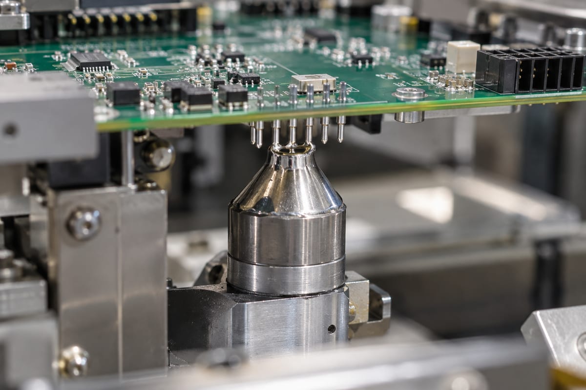
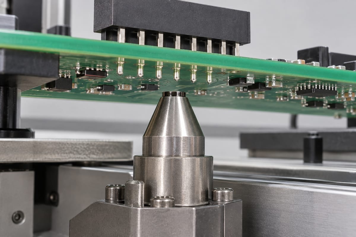
Selective wave soldering is the most common automated form of selective soldering used for through-hole PCB assembly. It creates a small, controlled wave of molten solder through a nozzle and brings that wave to specific joints.
The two terms are often used interchangeably in PCBA discussions, but they are not perfectly identical. “Selective soldering” is the broader description: solder is applied only where needed. “Selective wave soldering” identifies the localized mini-wave or nozzle method used to do it.
This distinction matters when requesting a quotation. A supplier may consider several routes for a difficult joint:
- a programmable selective mini-wave;
- a multi-nozzle or dedicated tooling arrangement;
- controlled hand soldering for very low quantities;
- a hybrid process in which accessible joints are automated and exceptional joints follow an approved manual method.
The drawing, quotation, or process agreement should therefore identify the intended manufacturing route when it affects cost, repeatability, inspection, or customer approval. For a closer look at the nozzle-based method, see EBest Circuit’s guide to selective wave soldering.
How Does the Selective Soldering Process Work?
The selective soldering process is a connected thermal and wetting sequence. Each stage influences the next, so a defect should not be blamed on the solder-contact step alone.
-
Flux application
Flux is applied to the selected area in a controlled pattern. It helps remove oxides and promotes wetting, but the amount and placement must suit the board, component leads, alloy, and cleaning requirements.
-
Preheating
Preheat activates the flux, reduces the temperature difference between the board and molten solder, and prepares high-mass joints to accept heat. A board with heavy copper planes, thick construction, or large connector pins may need a different thermal approach from a light, low-mass assembly.
-
Localized solder contact
The programmed nozzle approaches a pin, row, or joint group. Pump condition, nozzle geometry, solder height, travel direction, contact time, and withdrawal all affect solder flow and bridge formation.
-
Cooling and solidification
The joint must solidify without movement or unnecessary disturbance. Component stability, lead condition, and downstream handling can affect the result even after the solder leaves the nozzle.
-
Inspection and release
The completed joints are evaluated against the agreed workmanship criteria. The review should distinguish ordinary joints from thermally difficult pins because an acceptable connector corner may not prove that a plane-connected power pin has sufficient fill.
There is no universal temperature, dwell time, or travel speed that can be copied safely from another assembly. Surface finish, solder alloy, flux, board thickness, copper distribution, hole-to-lead relationship, component mass, and equipment configuration all change the process window.
Selective Soldering vs Wave Soldering: Which Fits the Board?
The correct choice comes from the board architecture and production economics—not from assuming that the more automated method is always better.
| Decision factor | Selective soldering | Wave soldering |
|---|---|---|
| Solder exposure | Chosen joints or groups | Most or all of the board underside |
| Typical board fit | Mixed SMT/THT assembly with limited THT locations | THT-heavy assembly or a board designed for broad wave exposure |
| Bottom-side SMDs | Can avoid many populated areas if access is available | May require adhesive, masking, a carrier, or a different layout |
| Joint quantity | Efficient when the programmed path remains reasonable | Usually faster when many accessible THT joints need soldering |
| Main setup | Program, nozzle selection, fluxing, and thermal profile | Wave profile, conveyor setup, pallet or masking when needed |
| Main limitation | Nozzle access and cycle time | Broad heat exposure and protection of non-wave-compatible areas |
| Changeover | Program and tooling may support variants | Pallets or masking may change with the assembly |
Selective soldering usually deserves serious consideration when reflowed bottom-side components sit near the required THT joints and only part of the assembly needs solder. It may also improve consistency for high-pin-count connectors that would otherwise require extensive hand soldering.
Wave soldering can be the better production route when the underside is designed for the wave, the board contains many THT joints, and conveyor processing provides a shorter cycle with acceptable protection and defect risk.
Controlled hand soldering can still be appropriate for prototypes, very low volumes, or isolated joints that a nozzle cannot reach. Its suitability depends on operator control, thermal demand, inspection, and the cost of variation—not simply on the number of boards.
Compare total production impact rather than one process price. Programming, tooling, masking, cycle time, touch-up, inspection, scrap exposure, and future product variants can change the better answer.
PCB Layout Limits: Nozzle Clearance, Thermal Mass, and Joint Access
A selective-soldering review should begin before the PCB layout is frozen. Once tall parts, bottom-side SMDs, connector bodies, panel rails, and copper planes are fixed, the available process window may already be too narrow.
Nozzle clearance
The nozzle needs physical space to approach the joint without contacting adjacent components or exposing them to unstable solder flow. The required keepout is equipment- and nozzle-specific; one universal clearance value should not be placed in a design rule without supplier confirmation.
Review the complete three-dimensional area around the joint, including connector overhang, component bodies, bottom-side packages, board fixtures, panel rails, and the nozzle’s travel and withdrawal path. A pad that looks accessible in a two-dimensional Gerber view may be blocked in the assembled board.
Thermal mass
Pins connected to ground planes, power planes, heavy copper, large pads, or substantial connector hardware can draw heat away from the joint. If the process is adjusted only for those difficult pins, nearby low-mass joints may receive excessive thermal exposure.
Thermal balance should therefore be considered at layout and validation stages. Plane connections, thermal relief design, finished hole size, lead diameter, board thickness, copper weight, and component mass all influence how quickly solder can rise through the plated barrel.
Joint access and solder flow
The lead, pad, solder mask, and hole must support wetting and drainage. Excessive lead protrusion can disturb the wave or encourage bridging; insufficient protrusion or an unsuitable hole-to-lead relationship may make solder flow and inspection more difficult.
The panel also matters. Rails, breakaway tabs, fixtures, and board support must allow the production system to hold the assembly consistently while keeping the required joints accessible.
Before releasing the design, ask the assembler to review the actual component models, board data, panel method, and intended nozzle. That review can reveal whether a layout change, different tooling, wave soldering, or an approved manual operation is more realistic.
Selective Soldering Defects: Bridging, Poor Barrel Fill, and Non-Wetting
Visible defects are outcomes, not root causes. Corrective action should connect the defect to the board condition, material state, and process stage instead of increasing heat or flux without evidence.
| Defect | What it may indicate | What to investigate |
|---|---|---|
| Bridging | Adjacent pins remain connected by solder | Pin spacing, lead protrusion, solder-mask geometry, nozzle path, solder height, travel direction, dwell, and withdrawal |
| Poor barrel fill | Solder does not rise sufficiently through the plated hole | Preheat, thermal mass, hole-to-lead fit, flux penetration, solderability, contact time, and blocked gas escape |
| Non-wetting | Solder does not form a reliable bond to the intended surface | Oxidation, storage condition, contaminated finish or lead, weak flux action, inadequate heat, and material compatibility |
| Icicles or peaks | Solder stretches during separation | Withdrawal behavior, travel speed, contact time, solder condition, and nozzle stability |
| Solder balls or splashing | Solder separates into unwanted deposits | Flux quantity, moisture, preheat, board condition, solder turbulence, and nozzle setup |
| Heat damage | Pad, mask, laminate, or component shows thermal stress | Excessive temperature or dwell, repeated repair, poor support, and an overly narrow process window |
Bridging on a connector does not always mean “too much solder.” The bridge may result from pin geometry, a poor travel direction, inconsistent board height, or a withdrawal path that pulls solder between adjacent leads.
Likewise, poor barrel fill is not solved reliably by extending contact time alone. A plane-connected pin may need more effective preheat, while another pin in the same connector could already be near its thermal limit. The process must satisfy both without creating a new failure.
Inspection should also consider residue, disturbed components, mask condition, pad damage, and evidence of repeated touch-up. If a joint repeatedly needs repair, the underlying layout or process window deserves review.
How to Validate Selective Soldering Before Production
Production validation should prove the process on the actual assembly, using the intended materials, program, tooling, and acceptance criteria. A machine demonstration on a different board does not establish that the released product is ready.
Start by defining what must be proven. The validation set should include the most difficult joints, not only the easiest connector row. Typical challenge points are plane-connected pins, large terminals, shielded areas, tight-pitch connectors, joints near bottom-side SMDs, and locations at the edge of nozzle access.
A practical validation sequence is:
- Confirm the PCB revision, BOM, component details, assembly drawing, panel arrangement, solder alloy, flux, and any cleaning restrictions.
- Review nozzle access and select the intended automated, wave, hand, or hybrid route for each THT location.
- Establish flux, preheat, solder-contact, travel, and withdrawal settings on production-intent equipment.
- Run a first article using representative boards and components.
- Inspect both normal and high-risk joints against the agreed criteria, including bridging, wetting, barrel fill, residue, and heat damage where applicable.
- Record the approved program, tooling, material set, inspection result, and any permitted touch-up method.
- Revalidate when a design, component, finish, alloy, flux, panel, tooling, or other controlled input changes enough to affect the process window.
Validation evidence should match the customer’s risk and contractual requirements. It may include first-article inspection records, visual results, process records, photographs, electrical testing, or additional analysis when specifically required. One document should not be treated as proof of every requirement: a process record confirms settings, while inspection or testing confirms the agreed output.
EBest Circuit can review assembly access and coordinate PCB fabrication, sourcing, SMT, through-hole processing, and agreed inspection or testing as part of its PCB assembly service. The released files and quotation should define the exact production and acceptance scope.

FAQs About Selective Soldering in PCB Assembly
1. When is selective soldering a good choice for a PCB assembly?
It is a good candidate when a mixed SMT/THT board has a limited number of through-hole joints, bottom-side components should avoid full-wave exposure, and the target joints have adequate nozzle access and a stable thermal window.
2. Can selective soldering replace wave soldering on every board?
No. A THT-heavy board may be faster and more economical to wave solder. Selective soldering can also be unsuitable when components, fixtures, or panel features block the nozzle, or when the programmed cycle becomes too long.
3. Is selective soldering always better than hand soldering?
No. It can improve repeatability and reduce operator variation for suitable joints, but controlled hand soldering may remain practical for prototypes, very low volumes, or exceptional joints that cannot be reached automatically.
4. What information is needed to assess selective-soldering feasibility?
Provide the released PCB data, drill and fabrication information, BOM with component details, placement and assembly drawings, panel requirements, order quantity, solder and cleaning restrictions, and the required workmanship, inspection, test, and traceability criteria.
5. What most often prevents a board from using selective soldering?
Common blockers include insufficient nozzle clearance, inaccessible joints, excessive thermal imbalance, unsuitable lead or hole geometry, obstructive panel tooling, and a production volume or joint count that makes another process more efficient.
Need a manufacturing review for selective soldering in PCB assembly? Send your released data, expected quantities, difficult THT locations, and acceptance requirements to sales@bestpcbs.com so EBest Circuit can compare the available PCBA routes for your project.