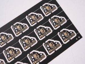
An AI robot power PCB distributes battery energy to processors, sensors, communications, motors, and safety circuits while keeping each rail within its permitted electrical and thermal limits. A board can pass a simple power-on check yet reset the compute module, corrupt sensor data, or overheat a connector when several actuators accelerate together. The sourcing package therefore needs a load profile, rail sequence, protection strategy, mechanical envelope, and acceptance plan before fabrication begins.

Are you worried about these problems in your AI robot power PCB project?
- Will motor startup or compute load steps pull a critical rail below its operating limit?
- Could connector heating, copper loss, or poor return routing create an intermittent field fault?
- Will incomplete test limits leave a prototype that powers on but cannot be released for production?
Founded in 2006, EBest Circuit provides one-stop PCB and PCBA manufacturing support from engineering review and prototyping through assembly and production.
- Load-profile review: We compare the supplied continuous, startup, regenerative, and fault currents with the proposed copper, connectors, protection parts, and assembly notes.
- Power-path review: We check the released input protection, converter placement, return paths, thermal interfaces, and high-current connections before prototype build.
- Test-scope review: We translate the approved rail limits, sequence, current draw, programming, and interface checks into a quotation-ready test requirement.
Ready to start your AI robot power PCB project? Send the current design package to sales@bestpcbs.com.
What Does an AI Robot Power PCB Control?
The board controls how energy enters, converts, branches, switches, measures, and shuts down across the robot. It may include reverse-polarity protection, surge or inrush control, fusing, DC-DC conversion, load switches, current sensing, rail sequencing, emergency-stop interfaces, and connectors for downstream modules. The exact boundary must be explicit: a power-distribution PCB is not automatically the battery-management system, motor controller, charger, or safety controller.
Map every source and load before selecting the construction. Record battery voltage over its full operating range, charger or docking input, motor and servo branches, processor rail, sensor rails, fans, lighting, and standby loads. For each branch, distinguish normal current, short transient current, repetitive peak current, and protected fault current. That separation determines connector selection, copper geometry, converter headroom, and the test equipment required.
How Should Robot Power Rails Be Planned Before Schematic Release?
Plan rails from the load envelope and permitted interactions, not from nominal voltage labels alone. Motors and servos create rapid and sometimes regenerative changes, while AI compute modules can impose sharp load steps. Cameras, encoders, and communication transceivers may require quieter references than the actuator bus. A shared source is possible, but uncontrolled shared impedance can turn one load event into another subsystem’s reset or measurement error.
- Source range: Record minimum, nominal, and maximum input voltage, hot-plug conditions, charger overlap, and the state after an emergency stop.
- Load envelope: Supply continuous, startup, repetitive peak, stall, sleep, and shutdown currents with their expected durations and concurrency.
- Rail priority: Identify which rails must remain alive for safe logging or controlled shutdown and which actuator outputs must turn off first.
- Noise boundary: Separate high-di/dt motor and converter loops from low-level sensors, clocks, and communication references.
- Fault ownership: State whether protection is handled by the battery pack, power PCB, downstream module, or a coordinated combination.
How Do You Size Copper, Vias, and Connectors for Robot Load Current?
Size the complete current path for temperature rise and voltage drop under the defined duty cycle. Trace width alone is not a release criterion. Current passes through connector contacts, fuse elements, copper neck-downs, vias, shunts, MOSFETs, solder joints, and cables. The weakest segment can dominate loss or heating even when the main plane appears generous.
Start with the approved current waveform and allowable drop at the load. Use the applicable PCB design method and supplier stackup to estimate external and internal copper behavior, then evaluate parallel layers, via arrays, terminal footprints, and heat spreading. Do not use a generic online trace-width result as proof of system capacity. Validate the assembled path at representative ambient temperature, airflow, enclosure contact, and duty cycle.
A practical review traces each branch from source pin to load pin and back through its return. Any pad entry, thermal-relief spoke, layer transition, or connector pin carrying the branch current must be included in the loss budget. Ask for finished-copper and hole requirements in the fabrication drawing rather than relying on an informal note.
How Should Input Protection and Fault Isolation Be Designed?
Protection should interrupt or limit a fault without exposing healthy rails to an uncontrolled collapse. The design may need reverse-polarity protection, transient suppression, inrush control, branch fuses or electronic protection, undervoltage behavior, overvoltage response, and a defined discharge path. Component ratings are only starting inputs; actual stress depends on the source impedance, wiring inductance, energy available, switching sequence, and thermal environment.
- Reverse connection: Specify whether a wrong battery connection must be blocked, tolerated without damage, or made mechanically impossible.
- Hot plug and inrush: Evaluate input capacitance, cable inductance, connector arcing, precharge, and the recovery behavior after a brownout.
- Branch fault: Coordinate each branch limit with wire, connector, copper, and load protection so a local short does not overheat an upstream path.
- Regenerative energy: Determine where motor-generated energy is absorbed or returned and what happens when the battery or charger cannot accept it.
- Emergency stop: Document which energy paths open, which control rail remains active, and how stored energy reaches a safe state.
How Does PCB Layout Reduce Motor Noise and Compute Resets?
Layout reduces interference by shrinking fast current loops, keeping their return paths local, and protecting sensitive rail references. Place each converter’s input capacitor, switch devices, inductor, output capacitor, and return according to the component manufacturer’s layout guidance. Keep switch nodes compact and away from clocks, camera interfaces, antennas, encoders, and external harness connectors.
The high-current distribution path and sensitive ground reference need a deliberate relationship. Splitting a plane without understanding the return current can force signals around a gap and increase coupling. Conversely, allowing motor current to share a narrow reference path with compute or sensor current can create ground movement. Review power and return together, including cable shields, chassis connections, mounting hardware, and test fixture grounds.
Verify the layout with simultaneous measurements of input voltage, affected rail voltage, branch current, reset or fault signals, and the failing interface. A quiet bench supply and idle motors do not represent acceleration, direction reversal, braking, or peak AI workload.
How Are Power Sequencing and Controlled Shutdown Verified?
Verify sequencing against the requirements of every processor, peripheral, and load switch across normal and abnormal power events. Some devices require one rail before another; others prohibit an input signal when their supply is absent. The shutdown path may also need enough stored energy and time for the processor to save data before the actuator bus disconnects.
- Document each state: Record off, standby, startup, run, charging, docking, emergency stop, brownout, controlled shutdown, and fault recovery.
- Set measurable limits: Specify rail thresholds, delay relationships, ramp expectations, power-good behavior, and maximum permitted reverse current.
- Test component tolerance: Repeat the sequence at input extremes and relevant temperatures using production-tolerance components or justified margins.
- Inject abnormal events: Remove input power, interrupt a branch, force an overload, and exercise repeated starts without bypassing protection.
- Correlate system response: Capture rails, enable signals, reset lines, current, and software event logs on a common timeline.
How Is Heat Managed on a High-Current Robot Power PCB?
Thermal control requires a continuous path from each loss source through copper, dielectric, vias, interfaces, and the enclosure or airflow. MOSFET conduction and switching loss, converter magnetics, rectifiers, shunts, connectors, and fuse elements can heat differently under steady and pulsed loads. A low-resistance copper plane can spread heat, but it does not prove acceptable junction or contact temperature.
Use loss estimates to select measurement locations, then correlate component temperature with current and operating state. The enclosure, mounting standoffs, thermal interface material, fan curve, neighboring boards, cable bundles, and ambient range all affect results. If a housing is part of the heat path, its contact area, flatness, fastener load, insulation requirement, and assembly process belong in the mechanical package.
Release limits should come from applicable component data and the robot’s reliability requirements. Measure the assembled module under representative workloads; an external PCB surface temperature alone cannot prove semiconductor junction temperature or connector life.
What Should Be Tested on an AI Robot Power PCB Prototype?
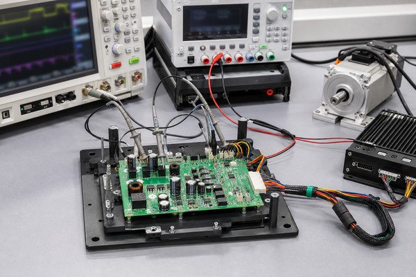
Prototype testing should connect each electrical requirement to a load condition, measurement point, limit, and failure response. Begin with safe unpowered checks, current-limited startup, rail accuracy, and programming. Continue with load steps, startup and stall profiles, sequencing, protection response, thermal behavior, and communication integrity. The robot-level test is still necessary because the harness, battery, motors, enclosure, software, and grounding can change the result.
| Test Group | Evidence to Capture | Decision Supported |
| Unpowered inspection | Polarity, resistance checks, assembly inspection, fixture identity | Whether controlled power-up can begin |
| Rail and sequence | Voltage, ripple, ramp, power-good, enable and reset timing | Whether compute and peripherals start in the intended order |
| Dynamic load | Input and rail waveforms during motor and compute load steps | Whether margin is adequate without nuisance reset |
| Protection | Trip threshold, response, recovery, stored-energy behavior | Whether faults remain within the approved boundary |
| Thermal | Current, duty cycle, ambient, airflow and component temperatures | Whether the assembled heat path meets its limits |
Use the table to agree on test ownership before quotation. A PCB assembler can verify the contracted board-level functions, while battery abuse testing, robot motion safety, final EMC, and complete machine validation remain with the responsible system organization unless specifically included.
How Is an AI Robot Power PCB Manufactured and Assembled?
An AI robot power PCB should move through a controlled fabrication, assembly, inspection, and electrical-release sequence built around its high-current paths and thermal mass. The released drawings and acceptance requirements—not a generic factory recipe—set the copper construction, soldering controls, inspection coverage, and test limits for each build.
- Release the fabrication and assembly package: Confirm the approved stackup, finished-copper requirements, Gerber or ODB++ data, drill and slot files, impedance requirements where applicable, panel drawing, surface finish, BOM, centroid data, assembly drawings, polarity markings, and acceptance criteria. Revision identity must match across the package; a mismatch can put the correct components on an obsolete board revision. Record the released file set and customer-approved deviations before tooling begins.
- Review high-current and thermal features for manufacturability: Check conductor widths, copper weights, neck-downs, via structures, copper-to-edge spacing, terminal holes, thermal pads, and heat-spreading areas against the released current and mechanical requirements. The fabricator should also review whether plating, etching compensation, drilling, routing, and panel support can hold the specified geometry. Unsupported geometry can create insufficient plating, etched neck-downs, damaged edges, or unstable component support. Resolve exceptions through an approved engineering query instead of changing copper or hole dimensions on the shop floor.
- Fabricate and electrically test the bare boards: Build the multilayer structure using the approved laminate system, image and etch the circuitry, form and plate holes, apply solder mask and legend, finish exposed pads, and route the final profile. In-process checks should verify material and lot identity, copper and dielectric construction, critical hole or slot dimensions, registration, plating quality, and surface-finish condition. Complete the specified bare-board electrical test so opens and shorts are removed before assembly consumes components.
- Prepare materials, tooling, and component traceability: Verify BOM revisions, manufacturer part numbers, approved alternates, date or lot controls when specified, moisture-sensitive-device handling, polarity, feeder setup, stencil revision, fixtures, and programming files. Large inductors, connectors, fuses, current-sense parts, and power semiconductors deserve an additional orientation and package check because an incorrect substitute or footprint assumption can change current capacity, thermal behavior, or protection response.
- Establish the solder-paste and reflow process: Match stencil apertures, paste volume, placement support, and thermal profile to the actual pad geometry and component mix. Heavy copper, exposed thermal pads, large terminals, and small control components can heat at different rates; insufficient energy may create incomplete joints, while excessive dwell or temperature can damage components or increase voiding. Approve the process from first-article solder-joint evidence and recorded profile data rather than from oven settings alone.
- Assemble surface-mount components under controlled programs: Print and inspect solder paste, place components with the released machine program, reflow the assembly, and preserve board and component traceability through the lot. First-article verification should confirm component identity, polarity, orientation, reference designators, and critical placement before the full batch proceeds. Any approved substitution or rework must remain linked to the affected serial number or production lot.
- Complete through-hole and mechanical operations: Fit high-current connectors, terminals, large inductors, heat spreaders, and other mechanically loaded parts using the specified selective, wave, press-fit, or documented manual process. Control solder fill, clearance, component seating, hardware sequence, and any drawing-specified torque or staking requirement. Fixtures or temporary support may be needed to prevent heavy parts from shifting or loading solder joints during processing. Record the completed operation, inspection status, and any approved rework against the affected unit or lot.
- Inspect workmanship and hidden power joints: Use visual inspection and AOI for accessible features, then apply X-ray or another approved method where thermal pads, bottom-terminated components, or obscured joints cannot be evaluated directly. Inspect for polarity errors, insufficient solder, bridging, disturbed joints, contamination, damaged mask, connector alignment, and the released void or solder-fill criteria where applicable. Record defects and rework history so recurring process drift can be separated from isolated workmanship errors.
- Run electrical and functional release tests: Begin with unpowered resistance, isolation, and short checks before applying energy. Continue with programming, rail sequencing, output-voltage and current checks, interface communication, protection or fault-response checks, and the customer-approved functional test at traceable limits. Release the assembly only when the test record, board revision, firmware or program version, material traceability, inspection status, and approved deviations all identify the same unit or lot.
What Files Are Needed for an AI Robot Power PCB Quote?
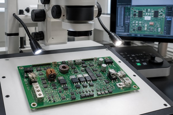
A useful quotation needs enough information to price the actual electrical, mechanical, assembly, and test scope. Gerber or ODB++, drill files, fabrication drawing, stackup, copper requirements, BOM, centroid data, assembly drawings, schematics, quantities, panel constraints, and approved alternates establish the board and build requirements. The power-specific package should add load profiles, connector and harness information, rail limits, sequence requirements, thermal interfaces, programming files, and test limits.
- Electrical inputs: Full source range, every output rail, continuous and transient current, duty cycle, fault behavior, and grounding scheme.
- Mechanical inputs: Board outline, mounting datums, connector access, component height, keep-outs, vibration constraints, and housing contact.
- Manufacturing inputs: Approved materials, finished copper, surface finish, workmanship criteria, traceability, change control, and packaging.
- Test inputs: Test-point drawing, programming package, fixture interface, loads, limits, sequence, logging fields, and report format.
Why Choose EBest Circuit for AI Robot Power PCB Manufacturing?
EBest Circuit gives you one manufacturing partner for DFM, PCB fabrication, component sourcing, assembly, and production. This keeps technical questions, revisions, materials, and production requirements under one coordinated project.
- Free DFM review: Identify manufacturability conflicts before tooling, reducing avoidable revisions, rework, and schedule disruption.
- Prototype-to-volume support: Keep the approved board revision, BOM, and manufacturing requirements consistent as order quantities grow.
- Flexible PCB construction: Evaluate FR4, multilayer, heavy-copper, metal-core, high-Tg, or impedance-controlled options against your power, thermal, and mechanical needs.
- Component sourcing and PCB assembly: Resolve PCB, component package, availability, and assembly questions through one coordinated supplier.
- Controlled change management: Track approved substitutions and production revisions so your team can reduce unexpected build-to-build differences.
- Inspection and testing to your requirements: Align the manufacturing plan with the acceptance criteria and test limits you provide, giving your team clearer release evidence.
FAQs About AI Robot Power PCBs
Q1: Should the robot power PCB include the battery-management system?
A1: It can, but the functional and safety boundary must be established first. A battery-management system monitors and protects cells, while a power-distribution board manages downstream branches and rails. Combining them may reduce connectors, but it also couples battery safety, charging, service, and robot power revisions. Confirm cell count, chemistry, charger, isolation, communication, protection ownership, and certification scope before combining the functions.
Q2: Is a four-layer PCB always required for robot power distribution?
A2: No; layer count must follow the electrical and thermal constraints. A simple low-current distributor may fit fewer layers; a mixed board with converters, compute interfaces, sensing, and controlled returns may need more. Compare candidate stackups using the actual current, copper, temperature-rise, EMI, and assembly requirements.
Q3: Can one DC-DC converter power all sensors and processors?
A3: Use one converter only if every load passes the same transient, noise, sequence, and fault limits. Separate rails or filters may be justified when a noisy load can disturb cameras, encoders, radios, or compute devices. Test the shared converter with simultaneous worst-case loads and representative harnesses before approving consolidation.
Q4: Where should current sensing be placed?
A4: Place the sensor at the electrical boundary that matches the required diagnosis or protection action. It may measure total battery current, a protected branch, converter input, or individual load output. Kelvin connections and return routing matter when using a shunt. Specify measurement range, bandwidth, accuracy, common-mode conditions, calibration, and fault survival rather than adding a sensor without a diagnostic purpose.
Q5: How should an emergency-stop input interact with the power PCB?
A5: The emergency stop must remove or control hazardous energy according to the machine safety design. Specify which loads lose energy, how actuators reach a safe state, and which monitoring or braking functions remain available. Do not assume that switching the logic rail or sending a software message removes hazardous energy. Verify contact behavior, stored energy, welded-switch faults, restart prevention, and the complete machine safety function.
Q6: Are thermal vias enough beneath power components?
A6: No; thermal vias alone do not prove an acceptable junction temperature. Their effectiveness depends on pad geometry, via construction, copper spreading area, solder process, airflow, and the external heat path. Use component loss and thermal data to build the model, then verify the assembled board under representative load and enclosure conditions.
Q7: When is an aluminum or metal-core PCB appropriate?
A7: Choose metal core when housing-directed heat spreading outweighs multilayer routing needs. It may be less suitable for dense multilayer routing, complex isolation, or many interconnections. Compare the complete thermal path, dielectric requirements, routing demand, assembly process, and mechanical interface rather than selecting by material label.
Q8: Can flying-probe testing replace functional testing?
A8: No; flying probe and functional testing cover different defect classes. Flying probe can check many opens, shorts, component values, and connectivity without a dedicated high-volume fixture, but it does not reproduce every powered operating state. Functional testing verifies rail behavior, sequence, interfaces, and load response under an agreed setup. Use the methods together according to defect coverage, volume, access, and test-time requirements.
Q9: What should be logged for each assembled power board?
A9: Log enough identity and measurement data to reproduce the test and isolate a failure. Include board and BOM revision, serial or lot, material and component lots where required, program version, test-station and fixture revision, measured results, operator or machine identity, deviations, and disposition. The record depth should match the product’s quality and traceability requirements.
Q10: How can a prototype avoid damaging an expensive AI compute module?
A10: Do not connect the compute module until every interface rail and protection response has been verified. Begin with unpowered checks and a current-limited source, verify polarity and each rail without the compute module, and use a representative load before connection. Confirm startup, shutdown, overvoltage, reverse-current, and fault behavior against the module requirements.
Conclusion
A reliable AI robot power board needs its load envelope, current paths, protection, rail sequence, thermal interfaces, manufacturing data, and acceptance tests to agree before production. EBest Circuit can help you turn those requirements into a buildable PCB and PCBA package, from prototype verification to repeat production.
Send us your design for a free DFM review and quotation. For a faster, more accurate AI robot power PCB review, include your Gerber/ODB++, BOM, stackup, quantities, load profile, mechanical data, assembly package, programming files, and test limits. Contact sales@bestpcbs.com to discuss your project and receive the manufacturing questions needed to move toward a controlled build.