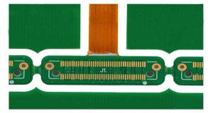
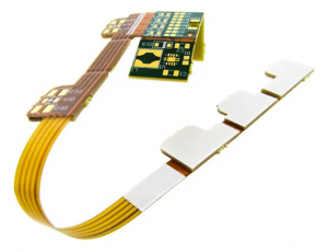
A rigid-flex PCB can look correct and still fail during installation, bending, assembly, or field use. Because rigid and flexible materials behave differently, the rigid flex PCB manufacturing process must join them without damaging the flex circuit or weakening its transitions. Here is where the main risks arise and what buyers should verify.

How Does the Rigid Flex PCB Manufacturing Process Work?
The process begins with the flexible inner circuit, protects the areas that must remain flexible, and then combines the flex and rigid sections.
A typical production sequence includes:
- Review the fabrication data, stackup, bend areas, coverlay, stiffeners, impedance requirements, and outline.
- Image, etch, and inspect the flex-layer circuitry.
- Apply coverlay and prepare the rigid cores and bonding materials.
- Lay up and laminate the rigid and flexible sections.
- Drill, clean, and plate the holes through the combined materials.
- Image and etch the outer layers, then apply solder mask and surface finish.
- Form the outline and expose the flexible areas.
- Complete electrical, dimensional, visual, and agreed reliability checks.
These operations interact: coverlay changes flex thickness, transitions affect bending, and prepreg and copper distribution affect resin flow. The stackup, mechanical drawing, bend definition, and manufacturing data must describe the same construction.
What Should You Confirm Before Rigid Flex PCB Manufacturing?
Before quotation, define whether the flex area bends once during installation or moves repeatedly in service. That choice affects copper, trace direction, layer count, coverlay, stiffeners, and bend geometry.
The fabrication package should identify:
- The controlled part number and revision.
- Rigid- and flex-layer construction, including controlled finished thicknesses.
- Static-bend or dynamic-flex use.
- Bend location, direction, available space, and installed shape.
- Material, copper, coverlay, transition, stiffener, and connector-contact requirements.
- Controlled impedance targets and the layers on which they apply.
- Surface finish, solder mask limits, testing, and required records.
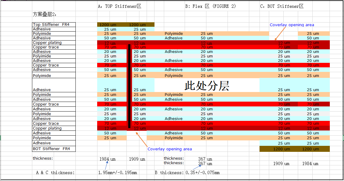
The bend drawing should define the inside radius, direction, movement type, and nearby rigid constraints. Compare the supplier’s production stackup with the fabrication drawing and impedance table; materials, copper, coverlay, and thicknesses should agree.
How Does the Rigid Flex PCB Fabrication Process Build the Flex Layers?
In the flex circuit manufacturing process, the flex layers are imaged, etched, protected, and inspected before final lamination. Thin materials need careful handling because they can stretch, crease, or collect contamination.
Key controls are:
- Trace routing: Smooth paths distribute bend strain; abrupt corners and copper buildup create stiff points.
- Coverlay: Film and adhesive affect flex thickness. Poor flow can leave weak sealing or obstruct openings.
- Transitions: Copper and coverlay changes near rigid edges should not create stress concentrations.
- Pre-lamination inspection: Conductor defects and coverlay misregistration are easier to correct before the flex layers are buried.
Any proposed opening, clearance, teardrop, or transition change should be marked in the DFM response. “Optimized for production” is too vague to approve.
How Does Rigid Flex PCB Fabrication Protect Drilled and Plated Holes?
During rigid-flex PCB fabrication, drilling and plating must create reliable connections through materials that move and react differently. Three checks matter:
- Registration: The drill must reach the target pad after imaging and lamination movement.
- Hole preparation: Debris and adhesive must be removed without attacking the flex dielectric.
- Plating: Copper must form a continuous connection to the internal features.
Risk is higher near transitions, with small annular rings, or with a thick board-to-hole ratio. Check finished holes, plating requirements, tolerances, and edge distances together. For demanding structures, a lot-related microsection is more useful than a generic certificate.
Which Flexible PCB Manufacturing Process Risks Affect Lamination?
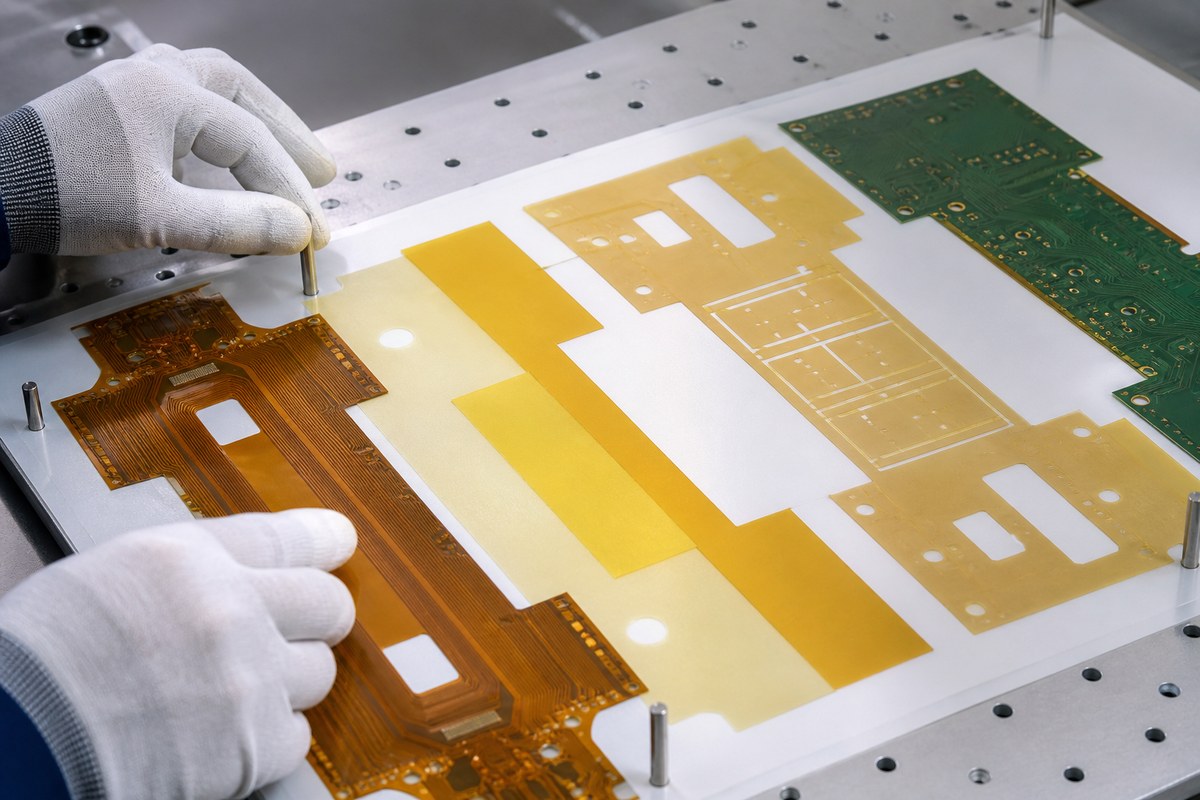
Lamination combines the rigid and flexible elements and locks in errors involving materials, registration, or resin flow. Bondply, coverlay, prepreg openings, no-flow prepreg, or release materials may be needed to keep resin out of flexible areas.
Several visible design details influence the result:
- Copper-density differences can change local resin flow and pressure.
- An unsuitable prepreg opening can flood the flex or starve a transition edge.
- Misregistration can shift rigid edges, coverlay, and copper features.
- Sharp stiffness changes can concentrate bending strain.
- Moisture or contamination can contribute to later delamination.
Approve a stackup that distinguishes rigid and flex regions and identifies materials, copper, adhesive, coverlay, and thicknesses. Any substitution should explain its effect on impedance, thermal requirements, and flexibility.
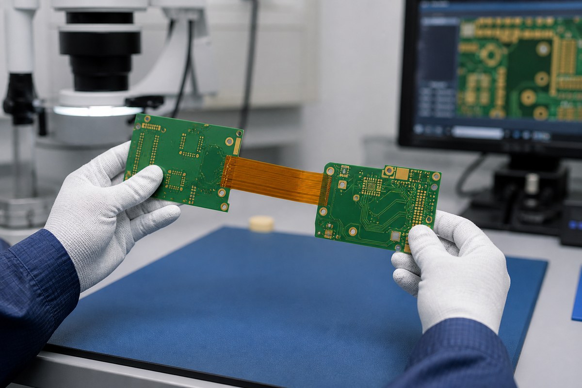
Which Rigid Flex PCB Fabrication Capabilities Should Buyers Verify?
For rigid flex printed circuit boards, evaluate capability against the actual design, not a factory’s broadest marketing number. A rigid flex PCB manufacturer should confirm that the proposed flex layers, thickness, holes, impedance, stiffeners, finish, and assembly fit a controlled process.
Useful capability questions connect directly to the design:
- What flex material, coverlay, and production stackup are proposed?
- How will the transition and exposed flex outline be formed?
- Which dimensions are controlled in the rigid, flex, and transition areas?
- How will impedance be modeled and verified across different regions?
- What inspection occurs before the flex layers are buried?
- Flex PCB assembly: If assembly is included, how will flex areas be supported during printing, placement, reflow, handling, and test?
A useful response identifies the construction, marks unresolved details, explains flex protection, and defines inspection. “Standard flex material” or confirmation of rigid thickness alone leaves mechanical assumptions open.
Where Do Inspection and Testing Fit in the Rigid Flex PCB Manufacturing Process Flow?
Inspection should follow the operation that creates each risk:
- Before lamination: Inspect flex circuitry and coverlay registration.
- After drilling and plating: Verify internal connections where the design requires evidence.
- After outer-layer processing: Inspect final conductors.
- After profiling: Check flex edges, slots, outlines, and transitions.
- At final test: Verify connectivity, isolation, dimensions, and agreed impedance requirements.
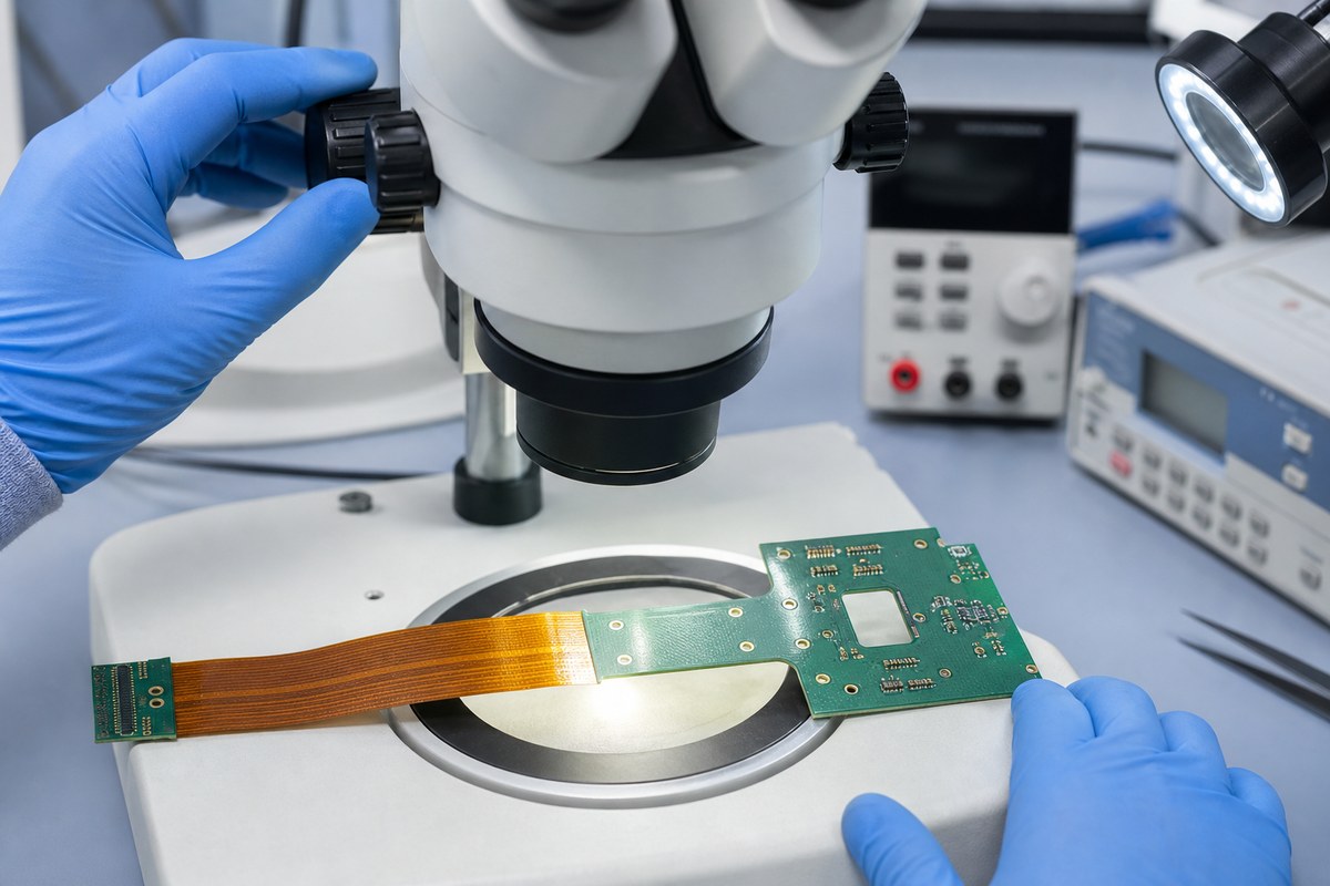
Electrical testing cannot prove material identity, flex thickness, coverlay registration, or internal plating quality. Define any required dimensional report, microsection, impedance result, or material record before ordering.
How Can the Rigid Flex Manufacturing Process Reduce Rework?
Rework often begins with conflicting outlines, transitions, stackups, or material assumptions. If the factory resolves the conflict internally, the board may differ from the intended design.
Use a closed-loop DFM review. Each question should point to a file, feature, layer, or requirement and end with one of three outcomes:
- The submitted requirement is confirmed without change.
- A marked manufacturing proposal is accepted and incorporated into the controlled release.
- The customer supplies corrected data and replaces the affected revision.
Do not close a question with “noted” or “please proceed.” Put any board-changing decision into the approved files. Before tooling, compare the file index, fabrication drawing, production stackup, and final DFM response, then close all remaining conflicts.
A Rigid-Flex PCB Example: From File Review to Production Release
Consider a six-layer board with four rigid layers, two flex layers, controlled impedance, and a tail folded once during installation.
DFM review identifies:
- No inside bend radius on the drawing.
- Different coverlay transitions on the two sides.
- No indication whether impedance applies in the rigid region, flex region, or both.
The engineer confirms the installed bend, controlled route, and transition geometry. The manufacturer returns a stackup showing completed flex thickness and impedance assumptions. After the files receive matching revisions, flex and coverlay inspection occurs before lamination; final dimensional, electrical, and impedance checks then verify the agreed construction. The three ambiguities are resolved before they become production defects.
FAQs About the Rigid Flex PCB Manufacturing Process
What information is most often missing from a rigid-flex PCB RFQ?
Bend use and installed geometry are commonly underdefined. State whether the flex bends once or repeatedly, show the direction and available space, identify stiffeners and transition locations, and provide the controlled stackup and acceptance requirements.
Why should the flex thickness include coverlay and adhesive?
Because bending behavior is affected by the completed flex construction, not only by the base dielectric. Copper, adhesive, and coverlay all contribute to local thickness and stiffness.
Can final electrical testing find every rigid-flex PCB defect?
No. Electrical testing can detect connectivity and isolation problems, but it does not prove correct material, flex thickness, coverlay registration, internal plating structure, or suitability for the installed bend.
When should a material substitution be approved?
Approve it before tooling or production, after the supplier identifies the proposed material and explains any effect on stackup, thickness, impedance, thermal requirements, flammability requirements, and flexibility.
What should be checked before repeat production?
Confirm that the released files, production stackup, approved DFM decisions, material substitutions, test requirements, and shipment records still match the last accepted revision. Do not rely only on a previous purchase-order number or an informal “same as last time” instruction.
Planning a rigid-flex prototype or production order? Send your Gerber or ODB++ data, drill files, fabrication drawing, stackup, bend requirements, impedance table, quantities, and inspection needs to sales@bestpcbs.com. EBest Circuit (Best Technology) can review the manufacturing package, identify open DFM questions, and prepare a quotation based on the confirmed project scope. Email the package for a review of your rigid flex PCB manufacturing process requirements.