If the gain falls during a VNA power sweep, do not report the first 1 dB drop as amplifier compression until you check the receiver. Repeat the sweep at the same calibrated DUT input powers with a different, characterized receiver-path attenuation. If the corrected compression point stays put within the uncertainty budget, it is evidence of DUT compression. If it moves, check receiver linearity, output loading and calibration before you accept either result.
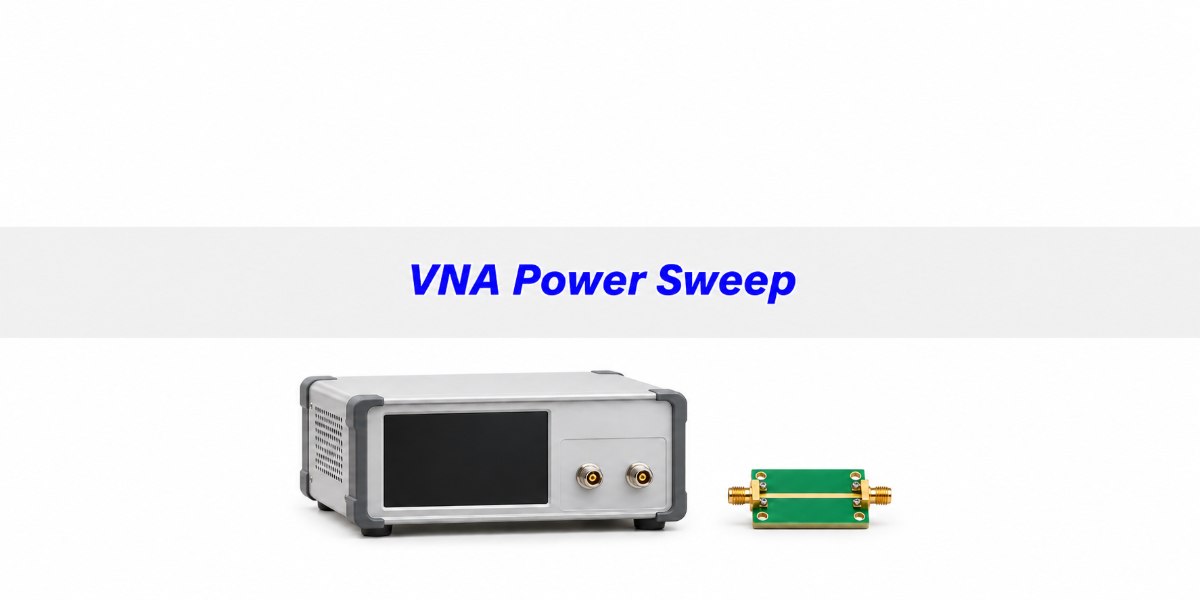
What Is a VNA Power Sweep?
A VNA power sweep changes drive level at one frequency while measuring how the response changes. A frequency sweep changes frequency at a specified stimulus level. Use the power sweep to find where fundamental gain stops being constant; repeat it at the frequencies where the product must meet its specification. A pass at one frequency does not establish compression across the band.
For a same-frequency amplifier, record calibrated incident input power and fundamental output power at the agreed DUT planes. With consistent wave/reference definitions, gain in dB is output dBm minus input dBm. A ratio trace can show the gain trend, but an ordinary small-signal S-parameter file does not establish absolute input power or describe a nonlinear amplifier at arbitrary drive levels.
Source Power Calibration: Put the Input Level at the DUT
Calibrate or verify source power at the DUT input plane, after input cables, adapters or a bias network that the test includes. The analyzer’s programmed output power is not necessarily the incident power at that plane. For a simple matched example, a −6 dBm source setting through 2 dB of input-path loss gives −8 dBm at the DUT. Use measured or calibrated power rather than applying a fixed loss correction over a range where loss, source leveling or mismatch is significant.
Use the instrument’s specified power-calibration method and verify the relevant range and frequency. Scalar power calibration establishes levels; vector error correction addresses systematic measurement errors such as match and tracking. Changing pads or reference planes may require a different calibration. Save the settings and reference planes with each sweep. Do not treat a single unchecked power-cal point or a changed cable as proof that the full sweep axis is correct.
Receiver Compression Point: Set a Safe Power Budget
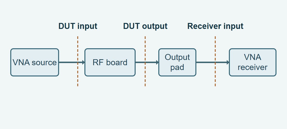
Pick attenuation and receiver range before applying RF. The analyzer’s damage limit and its linear measurement limit are different, and the lower usable power can depend on frequency, receiver range and test configuration. Check the source, both analyzer ports, the DUT, bias hardware, attenuators and any power sensor against their own RF and DC limits. Check reverse excitation as well: a full two-port measurement can drive the DUT output unless the instrument and setup are configured appropriately.
For a first estimate, suppose the maximum DUT-plane input is −6 dBm and the maximum credible gain for this example is 18 dB. The estimated DUT output is +12 dBm. If the selected receiver configuration has an illustrative linear ceiling of −2 dBm and you reserve 3 dB, aim for −5 dBm or lower at the receiver. The minimum estimated path loss is then 17 dB. With 20 dB of characterized loss, the estimated receiver input is −8 dBm. These values are arithmetic examples, not analyzer specifications. Check real maximum outputs, startup transients, attenuator rating, power dependence, and the lower noise limit before approving the setup.
Gain Compression Measurement: Establish a Linear Reference
Find several low-drive points with repeatable gain above the measurement floor, and use the reference method required by the test plan. Starting at the sweep’s lowest point is not enough if that point is noisy. Define compression as the amount the measured fundamental gain falls below the specified linear reference. Record any gain expansion rather than silently choosing the peak gain as a new reference; peak-gain and linear-gain definitions can give different crossings.
Stabilize bias, supply and temperature. Record bias current and wait conditions when changes in gain could come from self-heating or supply sag. A reverse sweep or a repeated low-drive checkpoint can reveal a history-dependent result, but it cannot identify temperature as the sole cause. If the product calls for pulsed rather than continuous-wave drive, use the specified regime and report pulse conditions separately.
1 dB Gain Compression Point: Calculate Input and Output
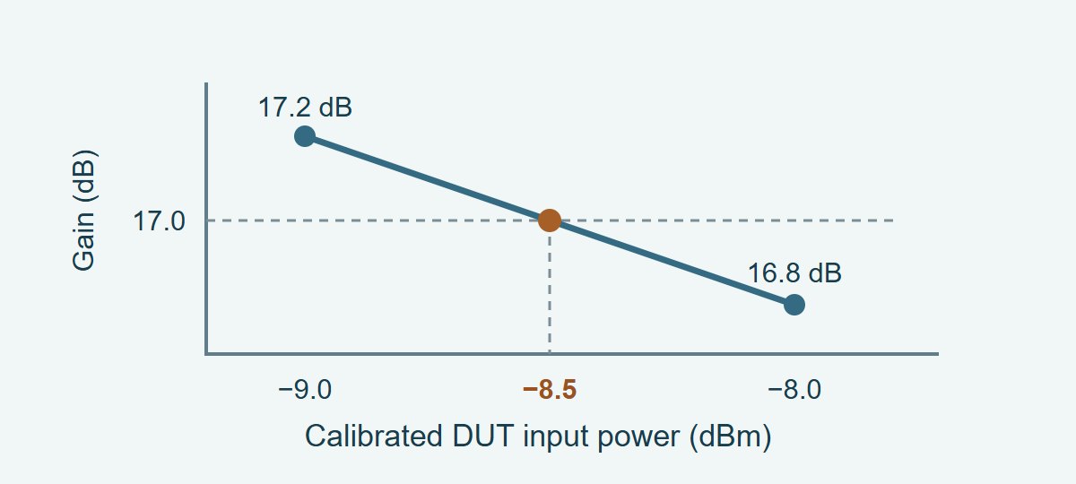
With 18.0 dB linear reference gain, target a measured gain of 17.0 dB. Suppose a valid calibrated sweep reads 17.2 dB at −9.0 dBm input and 16.8 dB at −8.0 dBm. Linear interpolation between those two points places the input crossing at −8.5 dBm; the corresponding output is +8.5 dBm, not +9.5 dBm. The latter is the output extrapolated from 18.0 dB of uncompressed gain. The values are illustrative, not measured amplifier specifications.
Take finer steps near the crossing before reporting a result close to a limit. Report whether P1dB is input-referred or output-referred, along with frequency, bias, temperature or stabilization conditions, and the applicable uncertainty. If the drive range never reaches the crossing under valid measurement conditions, report the verified bound rather than extrapolating a P1dB value beyond the sweep.
DUT Compression vs. Receiver Compression
Change receiver input power without intentionally changing the DUT input. Check that the alternate path neither changes the load materially nor shifts the reference planes; where possible use a verified downstream receiver attenuator arrangement. Recalibrate or correct each path, and verify both at low drive. If the additional attenuation reduces measurement margin, it can create a different error at the low-drive end. The two useful datasets need an overlapping region that is both above noise and below receiver nonlinearity.
| Observation | Likely problem | Check next |
| Same corrected crossing at the same DUT drive after an independent receiver-level change | Consistent with DUT compression | Verify the expected gain at low drive, comparable DUT load, and sufficient margin in both sweeps |
| Droop starts earlier only with the higher receiver level | Possible receiver compression | Confirm receiver linearity and path corrections with a suitable reference at comparable receiver powers |
| Low-drive baseline changes with the pad even though both receiver levels are verified linear | Load mismatch, changed reference plane or path loss | Verify pad response, load seen by the DUT, connector repeatability and correction state |
| Gain wanders at the low-drive end, worse with more attenuation | Weak-signal uncertainty | Check noise and repeatability before changing the reference gain |
If low-level gain has no flat, repeatable region, use the VNA IF bandwidth and noise-floor checks before collecting the compression sweep. Narrowing IF bandwidth may help a noisy baseline; it does not fix an overloaded receiver.
VNA Power Sweep Setup for Amplifiers, Filters and Fixtures
RF amplifier board: Place both DUT planes at the agreed RF interfaces. Check bias under drive, measure at the required frequencies, and verify the crossing using a second corrected receiver level. Accept when its position is repeatable under the specified bias and drive regime and meets the product limit after applying the agreed decision rule.
Passive RF filter: When checking whether insertion loss changes with drive, choose frequencies inside the passband and separately check stopband measurement margin. Keep incident power within the product’s conditions. Accept only if repeatable changes stay inside the allowed variation over the stated level range. A stable low-power sweep does not qualify the component for higher-power service.
Test fixture or path: Use a characterized linear thru or attenuator with adequate rating to check the chain over the levels it must measure. Match receiver levels as well as practical; replacing a high-gain amplifier with a bare thru at the same source level alone does not exercise the receiver at the same power. Require stable corrected response in the overlap region before blaming the board.
Gain Compression Test Report: Log the Evidence
Fill one row per frequency and test condition, then check that the conclusion survives the second setup. The example below shows what a complete record should contain. The illustrated crossing is not a passing result unless the product requirement and uncertainty rule agree.
| Record | What to write and verify |
| Test conditions | Frequency, sweep direction and steps, bias and current, CW or pulse settings, DUT serial and both physical reference planes |
| Baseline and bracket | Example: 18.0 dB linear reference; −9.0 dBm/17.2 dB and −8.0 dBm/16.8 dB; input −8.5 dBm and output +8.5 dBm by local interpolation |
| Independent setup check | Two corrected receiver-path configurations; actual linear range and noise margin; record the corrected crossing from both, not just the selected trace |
| Disposition | Applicable limit and whether it is input or output, uncertainty or guard band, power margin checks and any untested frequency or condition |
VNA Power Sweep FAQs
Should I keep the same source setting when I change the output pad?
Keep the same verified DUT input power, which is the quantity that matters. Also confirm the alternate path has not changed DUT output loading enough to alter the amplifier’s actual behavior.
Why does the measured compression point move when I add an attenuator?
Possible causes include analyzer nonlinearity, an uncorrected pad response, changed load match or a different usable signal range. Check a characterized reference and compare at the same DUT input powers before interpreting the shift.
Does a 1 dB gain drop mean a 1 dBm output power?
No. One dB is the difference from reference gain. P1dB can be any absolute input or output power in dBm within the specified test conditions.
Can I measure P1dB from a frequency sweep at one power?
Not generally. You need a valid gain reference and enough drive levels at the frequency to bracket the crossing, or an instrument mode that performs this sweep at each selected frequency.
Can I use only an RF generator and a power meter?
Yes, if you establish the incident drive and the relevant output with suitable calibrated equipment. If the output sensor sums harmonics but the specification concerns only fundamental power, use a validated frequency-selective method or filtering.
Does the VNA receiver always compress right before it is damaged?
No. The input may remain undamaged while measurement errors are already unacceptable. Consult the linearity and protection limits for the exact receiver path and instrument configuration, and check both.
What if no compression appears in the validated sweep?
Report that the crossing was not reached within the verified range and state its upper tested drive. Confirm that the reference gain and power readings remain valid at the highest tested point.
Can lower IF bandwidth replace output attenuation?
No. It can improve repeatability near the noise floor but does not lower incoming RF power. Select attenuation and range to maintain receiver linearity, then choose bandwidth for the resulting signal level.
Technical References
- Keysight Gain Compression Application — reference gain, receiver compression precautions and setup options.
- Keysight Power Calibration — power correction and reference plane for a model-specific implementation.
- Keysight Receiver Compression Performance Test — why receiver linearity is a separate verification.
- Rohde & Schwarz amplifier characterization application note — calibrated gain, input power sweep and receiver attenuation options.
Custom RF PCBs With Stackup and Test Access Review
Send EBest Circuit your fabrication files, target stackup and controlled-impedance requirements. Flag the connector interfaces, any de-embedding or coupon arrangement, and the test access you need before fabrication. The more clearly your files define those interfaces, the easier it is to agree on a build and verification scope before ordering. Email sales@bestpcbs.com to request a custom RF PCB quote.