Use VNA isolation calibration only when a stable leakage path is large enough to affect the result and the correction improves an independent check. The optional step measures transmission with the two test ports terminated separately. It can reduce stable additive leakage in the calibration model. It cannot recover a signal buried in random noise or separate physical PCB crosstalk from the PCB you intend to measure.
Start with each port on its own matched load. Save the complex trace, then verify the result with a known attenuator in the range you intend to claim. If the corrected trace looks deeper but a check standard disagrees, do not use the nicer-looking stopband.
VNA Isolation Calibration: What the Optional Step Removes
There should be no intentional transmission path between independently terminated ports. A repeatable response can still appear because part of the source signal reaches the receive path. On a VNA that implements an isolation term, that leakage becomes an additive error estimate. A two-port calibration can have separate forward and reverse isolation estimates.
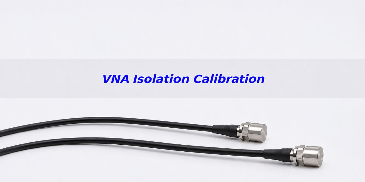
Thinking in complex numbers explains the limit. If M is the measured response, D the wanted response, and L an additive leakage term, the simplified model is M ≈ D + L. The correction estimates and removes a vector, not a number of decibels. This picture isolates one error mechanism; it is not the complete two-port error model.
VNA Crosstalk Measurement: Separate Three Leakage Paths
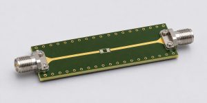
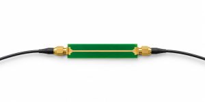
First decide where the unwanted signal travels. Measure with the cable ends separately terminated, then compare a fixture isolation witness with the intended launches, cable routing, switch states and unused ports. A witness can be an intentionally isolated coupon designed to preserve the fixture geometry. Its result characterizes that witness; it does not automatically equal the leakage when a real PCB is installed.
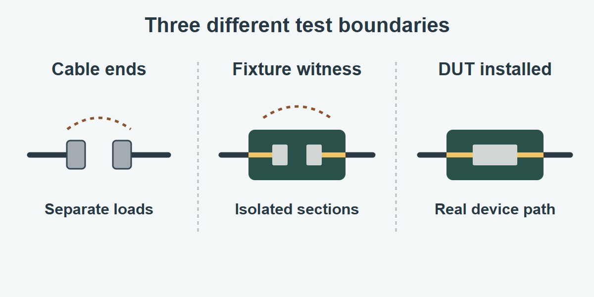
| Path | Check | Action |
|---|---|---|
| Analyzer and cables | Two independent loads. | Try isolation correction if the residual is stable. |
| Fixture or switch path | Matched isolated witness. | Fix or validate the fixture separately. |
| PCB coupling | Actual board and required terminations. | Keep it if this coupling is the thing being measured. |
VNA Calibration Procedure: Terminate Both Test Ports
- Define the planes and conditions. Record the port map, frequency grid, source power, receiver settings and reference impedance. Use 50 Ω loads only for a setup whose calibration and test plan call for them.
- Follow the instrument’s calibration sequence. At the isolation prompt, put a separate matched load on each indicated test port. Do not use an open cable, a thru, or the DUT in place of an isolation standard.
- Acquire a clean estimate. Use the approved IF bandwidth or averaging setting for the calibration. Hold cable positions and switch states stable. Save the calibration and record whether both directions were acquired.
- Keep a comparison calibration. Where the instrument supports it, compare equivalent calibrations with and without the isolation term. Do not deliberately change receiver range or source power at the same time; it defeats the comparison.
VNA Noise Floor: Decide Whether Isolation Correction Helps
Repeat the terminated sweep and look at complex consistency. If a response is repeatable at the same frequencies and keeps phase across sweeps, a stable term may be present. If the response varies strongly in phase and magnitude near the floor, subtracting a noisy estimate can add error. A lower displayed trace after calibration is not by itself a reason to keep the term.
Use the VNA IF bandwidth guide when the problem may be random noise and sweep time rather than a stable leakage term. Verify a new calibration if instrument settings or the physical setup change. Never assume that a narrower bandwidth removes coherent leakage.
S21 Measurement: Convert Leakage Separation to an Error Bound
A leakage residual 20 dB below the wanted signal can still shift its reading by about −0.92 to +0.83 dB. For a calculated example at one frequency, assume S21 for the DUT is −80 dB and the remaining leakage bound is −100 dB at the same plane and normalization. The residual-to-wanted amplitude ratio is 10−20/20 = 0.100.
For a coherent residual with unknown phase, the extreme magnitudes are 0.900× and 1.100× the wanted amplitude. Convert those ratios with 20 log10. If you allocate no more than ±0.5 dB to this one error source, the more conservative cancellation case requires a ratio no greater than 1 − 10−0.5/20, or about 0.0559. That corresponds to 25.1 dB separation when rounded conservatively. Neither figure includes random noise, calibration-match error or repeatability.
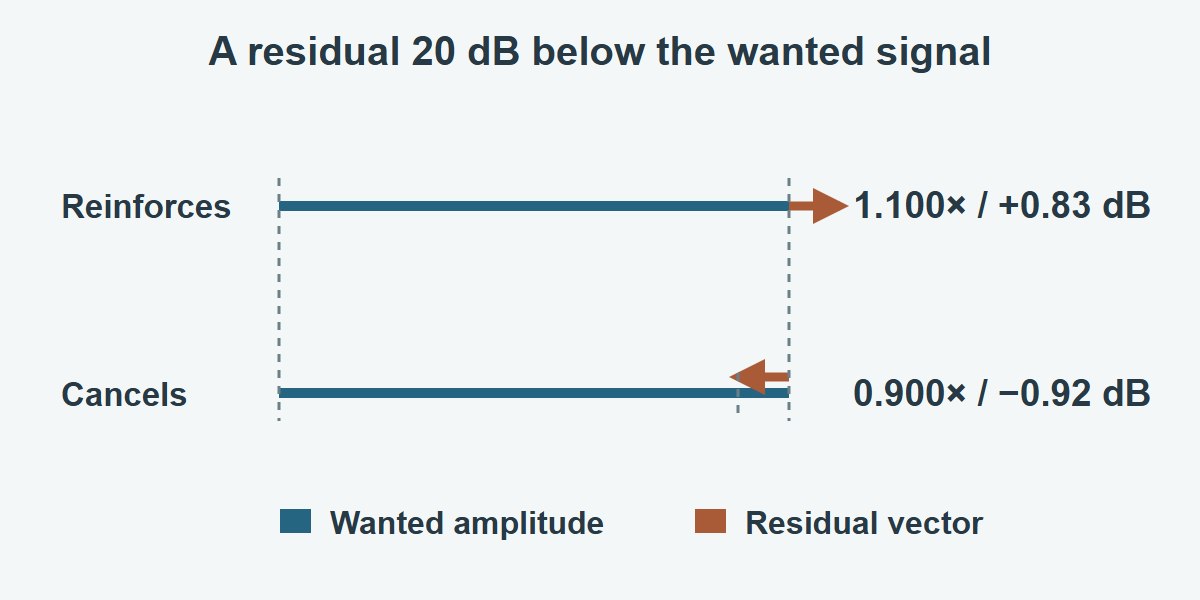
Use a justified upper bound on residual leakage, not the easiest single terminated sample. If you do not know the wanted amplitude independently, work from the product limit as a design target for the measurement or use the verified complex error bound and the applicable decision rule. Do not label the example separation as a full uncertainty budget.
VNA Calibration Standards: Verify With an Attenuator You Did Not Fit
Choose a characterized attenuator whose attenuation, reference plane, frequency range and uncertainty are appropriate to the decision. Measure it in both directions if both are in scope. Compare the result using each candidate calibration, with the same cables, band and test settings. Reconnect once or more under the approved repeatability procedure to see whether the claimed improvement survives re-mating.
A thru can verify basic tracking, but it cannot establish deep-attenuation accuracy. A low-loss reference is not a substitute for verification near −80 dB if that is what you intend to report. Do not assume a chain of nominal pads has the precise sum of its labels across the band. If the verification does not cover the required level, improve the setup or report the unverified band explicitly.
After both directions have enough verified margin, use the S21 vs. S12 guide to compare their complex responses. Do not interpret a direction-to-direction difference below the validated floor as nonreciprocal PCB behavior.
RF Isolation Measurement: Apply the Check to Three PCB Tasks
Filter stopband
Keep the filter and any shielding that belongs to the product in the measurement path. Compare the isolated fixture witness and attenuator before the sweep. Release only the frequencies at which the verified leakage and noise allowance supports the specified stopband limit; do not call the display floor the filter response.
Coupling between RF traces
Drive the defined aggressor and measure the victim at the specified end, with the other ports in their required terminations. Compare a fixture witness using the same cables and orientation. Do not subtract the coupling between PCB traces you came to measure, or report a matched-port result as a guarantee for an unmatched deployed load.
RF switch off-state
Keep the intended off-state, bias and unused-port terminations. Characterize or eliminate leakage around the fixture and through the switch matrix used for measurement. Verify representative off-state attenuation and repeat the state transition at the approved power; do not assume an open bench condition verifies off-state isolation.
VNA Dynamic Range: Decide What the Report Can Claim
Use the worksheet for the weakest relevant part of the band. Include both port directions when required and record the path used to establish the leakage bound. Document the product limit and chosen guard band separately from the calibration steps.
| Check | Example | Decision |
|---|---|---|
| Leakage allowance | −80 dB wanted, −100 dB residual bound. | 20 dB gap is insufficient for the example ±0.5 dB allowance. |
| Independent reference | Enter known attenuation, band and uncertainty. | Verify both directions required by the test plan. |
| Reporting limit | Save settings, witness, repeats and unsupported band. | Report unresolved points as inconclusive, not a precise pass. |
For RF PCB test acceptance, use the drawing, contract and qualified test plan for limits and uncertainty. There is no universal PCB isolation-calibration separation to substitute for them. If you cannot distinguish the DUT from the setup, retain the raw and corrected data and state exactly what remains unproven.
VNA Isolation Calibration FAQs
Do I need two matched loads?
Use the termination procedure for your model. The conventional two-port isolation step described here uses separate matched loads at the indicated planes.
Can I skip isolation calibration?
Yes if your method allows it and independent verification shows that residual leakage and uncertainty meet the measurement need.
Is S21 in dB the same as a positive isolation number?
Not in sign: for the same transmission path, S21 of −80 dB is often described as 80 dB of isolation. Record both the path and sign convention.
Why did my trace become noisier after calibration?
The correction can include noise from its estimate. Repeat at documented settings, check an independent reference and compare a calibration without isolation.
Can I subtract the terminated plot in dB?
No. Coherent leakage adds as a complex amplitude and may reinforce or cancel the wanted signal.
Can I use the same correction after moving a cable?
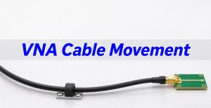
Only if your procedure verifies it still applies. Movement can alter both transmission tracking and leakage.
Will an isolation correction remove fixture crosstalk?
Not generally. Leakage that changes with the installed DUT or setup is not a stable matched-load term. Verify the actual fixture separately.
How much separation should I require?
Derive it from the allowed error and the verified type of residual, then include the other uncertainty sources. Do not treat the example as a specification.
Technical References
- Keysight PXIe VNA: Accurate Calibrations — optional isolation, matched loads and near-floor limitations.
- Keysight PXIe VNA: Crosstalk — acquisition of leakage and noise reduction.
- Keysight: Calibration Standards — forward and reverse transmission error classes.
- Siglent: Calibration and RF Measurements Using VNA, Rev. 8 — calibration and RF test setup.
Custom RF PCBs With Stackup and Test Coupon Review
Planning a filter, switch or multi-channel RF PCB? Send EBest Circuit your stackup, Gerbers or ODB++, launch parts, frequency band and the locations of the isolation checks. Reviewing the launch and coupon geometry before fabrication helps make board results and fixture results comparable.
Request an RF PCB fabrication quote with your quantity, required date and acceptance plan.