A PCB trace inductance calculator estimates the inductance added by a copper connection. Enter the trace length, width and finished copper thickness for an isolated straight-strip estimate. For a trace with a defined return plane, select the transmission-line model and enter the characteristic impedance and effective relative permittivity for that stack-up. The two results describe different electromagnetic conditions and should not be substituted for each other.
PCB Trace Inductance Calculator
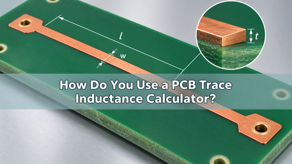
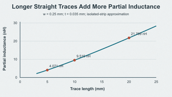
The default inputs in this online PCB trace inductance calculator are a 10 mm long, 0.25 mm wide trace with 35 micrometer copper. Its estimated partial self-inductance is 9.515 nH. Changing a length unit preserves the entered physical dimensions.
What Is PCB Trace Inductance?
PCB trace inductance is the property that produces an induced voltage when current through a copper interconnect changes. Its calculated value depends on how the return conductor is represented: an isolated segment’s partial inductance is not the same quantity as the inductance of a complete current loop.
The straight-strip mode is a PCB trace self inductance calculator for one uniform rectangular conductor. It estimates partial inductance with the return sufficiently distant that nearby conductors are not included in the model. Used as a PCB trace parasitic inductance calculator, it describes that segment’s contribution; a complete circuit also has a return conductor and magnetic coupling between paths.
The known-transmission-line mode derives equivalent inductance and capacitance from the line’s supplied impedance and propagation velocity. It is useful when a stack-up calculation or extraction has already provided those parameters. It does not solve microstrip geometry, vias, bends, pads or a split reference plane.
What Inputs Are Needed to Calculate PCB Trace Inductance?
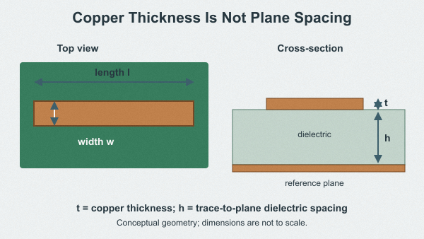
Use the conductor’s routed length, finished trace width and finished copper thickness. Copper thickness t is different from dielectric height h, which is the spacing between the trace and its reference plane.
| Input | Use this value | Common error |
|---|---|---|
| Length l | Length of the uniform straight conductor segment | Using the board dimension or including a via without changing models |
| Width w | Finished copper width for that segment | Using pad width for an otherwise narrow trace |
| Copper thickness t | Finished conductor thickness in micrometers or mil | Entering the trace-to-plane spacing as copper thickness |
| Effective relative permittivity | Effective value for the selected transmission-line geometry | Automatically substituting the laminate’s bulk Dk for a microstrip effective value |
One mil is 0.0254 mm, one inch is 25.4 mm and 35 micrometers is 0.035 mm. Nominal 1 oz copper is commonly close to 35 micrometers, but outer-layer plating and the released fabrication stack-up determine the finished value.
How Is PCB Trace Inductance Calculated?
For a long, isolated rectangular strip, the approximation used here is:
L [nH] = 0.2l {ln[2l/(w + t)] + 0.2235(w + t)/l + 0.5}
All three dimensions are in millimeters and ln is the natural logarithm. The equivalent coefficient is 0.0002 when the result is expressed in microhenries. Mixing that coefficient with a nanohenry output creates a factor-of-1,000 error.
When calculating PCB trace inductance, length has a stronger effect than the same proportional change in width or thickness. This implementation uses a conservative input limit of l at least 10 times (w + t) so that short, broad pads are not silently treated as long strips. That is a tool limit, not an IPC acceptance criterion. The approximation excludes nearby return conductors, skin effect and mutual coupling.
How Much Inductance Does a 10 mm PCB Trace Have?
A 10 mm trace with w = 0.25 mm and t = 0.035 mm gives 9.515 nH in straight-strip mode. At 100 MHz, its corresponding inductive reactance is 5.978 ohm. These are model results, not measurements from a fabricated board.
| Length | Width | Copper thickness | Partial inductance |
|---|---|---|---|
| 5 mm | 0.25 mm | 35 micrometers | 4.071 nH |
| 10 mm | 0.25 mm | 35 micrometers | 9.515 nH |
| 20 mm | 0.25 mm | 35 micrometers | 21.789 nH |
| 10 mm | 0.50 mm | 35 micrometers | 8.266 nH |
In this example, halving the length cuts the estimate by about 57%, while doubling the width cuts it by about 13%. Widening copper still helps current capacity and resistance, but it does not halve the inductance.
How Does the Return Path Affect PCB Trace Inductance?
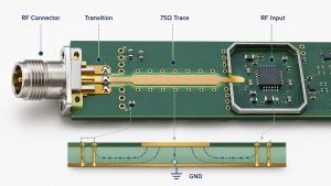
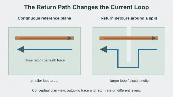
Current returns to its source. A close, continuous reference plane keeps the outgoing and returning paths near each other, reducing the area of the current loop. A plane split, connector transition or remote return can force current around a much larger path.
A PCB trace loop inductance calculator must therefore account for both conductors and their coupling. The isolated-strip result cannot establish the loop inductance of a decoupling connection or switching-power hot loop. A parallel plate inductance calculator describes another geometry again; its assumptions cannot be applied to every narrow PCB trace.
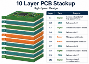
For multilayer FR4 PCB layouts, the trace-to-plane dielectric spacing is often more useful to review than overall board thickness. Two 1.6 mm boards can have very different signal-layer spacing and return geometry.
How Do You Calculate Inductance for a PCB Trace over a Ground Plane?
For a uniform, low-loss line, characteristic impedance and propagation delay relate directly to distributed inductance and capacitance:
Delay = l sqrt(effective relative permittivity) / c
L = Z0 x delay
C = delay / Z0
In these relations, l is in meters, c = 299,792,458 m/s, delay is in seconds, Z0 is in ohms, L is in henries and C is in farads. The calculator performs the conversions to nH, pF and ns.
For an assumed 50 ohm line, effective relative permittivity 3.2 and length 10 mm, the results are 2.983 nH, 1.193 pF and 0.05967 ns. The comparison with the isolated-strip example demonstrates model sensitivity; it is not a claim that the example strip’s width automatically produces a 50 ohm line.
A geometry-based microstrip inductance calculator also needs the trace-to-plane spacing and dielectric information. A stripline inductance calculator needs the appropriate buried-line geometry. In this tool, those effects must already be represented by the supplied Z0 and effective relative permittivity. The line option therefore works as a PCB trace inductance and capacitance calculator for known line parameters. Use a field solver when those parameters have not been established.
A microstrip capacitance calculator uses the same conductor and dielectric structure. A PCB trace impedance formula based on the wrong cross-section also gives the wrong Z0 input; confirm whether the route is microstrip or stripline before using its result.
How Do You Calculate PCB Trace Inductive Reactance?
The displayed reactance uses XL = 2pi fL. Setting frequency to zero produces zero inductive reactance in this idealized model; it does not remove copper resistance. Changing frequency does not recalculate skin effect or frequency-dependent material properties.
For the 9.515 nH straight-strip example, the reactance is 0.598 ohm at 10 MHz and 5.978 ohm at 100 MHz. The frequency change alters reactance; it does not change the inductance returned by this geometry-only approximation.
How Does PCB Trace Inductance Cause Voltage Spikes?
The transient estimate uses V = L x delta I / delta t. For 9.515 nH and a 1 A change in 1 ns, the lumped estimate is 9.515 V. With a 10 ns current transition, it falls to 0.9515 V. This explains why fast switching edges can make short connections important even when the switching repetition rate is modest.
The complete switching loop includes packages, capacitors, vias and return paths. If one-way propagation delay is no longer small compared with the rise time, use distributed transmission-line analysis. The tool flags a delay exceeding 10% of rise time as a screening reminder, not as a universal compliance limit or a measured-overshoot prediction.
How Can You Reduce PCB Trace Inductance?
Shorten the complete current path and keep its return close. Increasing copper width alone has diminishing benefit for the isolated-strip estimate.
- Place high-frequency decoupling connections close to the supply and return terminals they serve.
- Keep critical routes over continuous reference copper and check how return current crosses a layer transition.
- Reduce unnecessary detours, long stubs and connector excursions before increasing copper area.
- Review the whole power loop, including component pads, package connections and vias.
- Use coupled extraction when adjacent conductors or multiple return paths determine the result.
Where shorter interconnects require HDI PCB construction, we can review blind-via and microvia options with the proposed stack-up. HDI does not automatically guarantee lower inductance: the actual via geometry, return vias and layer arrangement still govern the connection.
How Do PCB Trace Tolerances Affect Inductance?
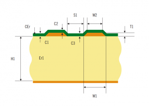
Finished trace width and copper thickness set the w and t inputs in the straight-strip formula. Etching and plating can change those dimensions from their nominal design values. In a ground-referenced transmission line, dielectric spacing and conductor geometry also affect Z0 and effective relative permittivity. Use the released stack-up and finished geometry rather than assuming that nominal copper weight or overall board thickness defines these inputs.
At EBest Circuit (Best Technology), we can review the intended stack-up, finished conductor geometry and impedance-controlled PCB requirements before fabrication. We support standard FR4 line/space down to 4/4 mil and HDI options down to 2/2 mil, subject to stack-up, materials, board dimensions and engineering review.
For a calculation that will influence layout release, identify the signal layer and reference plane, dielectric spacing, material data, finished copper thickness, trace-width tolerance, route length and transitions. For controlled-impedance work, specify the target and acceptance method as well. An impedance coupon verifies a transmission-line requirement; it does not directly certify the inductance of every assembled current loop.
A PCB trace current calculator or PCB trace resistance calculator answers a separate design question. Check current capacity, voltage drop and thermal behavior alongside inductance instead of expecting one trace-size result to establish all four.
PCB Trace Inductance Calculator FAQs
Why do two PCB inductance calculators give different answers?
A PCB inductance calculator may use different conductor geometry, return-path assumptions, units or copper-thickness conventions. Compare those inputs before comparing the output. A flat wire inductance calculator and a microstrip model do not describe the same field distribution.
Does this tool calculate via inductance or mutual inductance?
No. Use a geometry-specific via inductance calculator for a via estimate. A PCB trace mutual inductance calculator also needs relative conductor positions, separation, coupling and return paths; one trace’s length, width and thickness are insufficient.
Can I use this to design a spiral PCB inductor?
No. A PCB trace inductor calculator for a spiral needs turn count, inner and outer dimensions, spacing and winding shape. Adding straight-segment partial inductances does not include the mutual coupling between turns.
Use the PCB trace inductance calculator with the model that matches the connection: isolated straight strip for a partial-inductance estimate, or known line parameters for equivalent transmission-line inductance and capacitance. Preserve the units and check the return path before treating the number as a circuit-level result.
For fabrication review, send your PCB files, proposed stack-up, critical route information and impedance requirements to sales@bestpcbs.com. We can check the manufacturable trace geometry and stack-up inputs with you before production.