





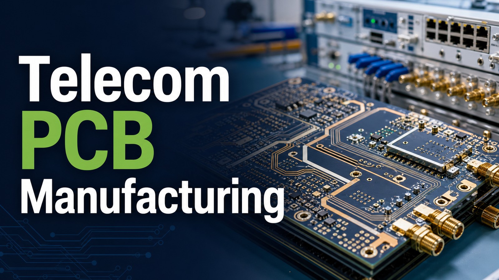
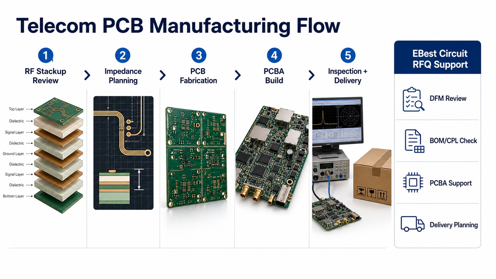
Telecom PCB manufacturing services help buyers turn RF, high-speed and network hardware designs into manufacturable PCB or PCBA builds. The supplier should review stackup, material choice, impedance targets, RF routing constraints, component placement, inspection needs, packaging and delivery planning before the quotation is treated as final.
For telecom buyers, the useful question is not only who can fabricate the board. It is whether the supplier can connect engineering review, PCB fabrication, optional PCBA, testing expectations and repeat-order planning in one clear RFQ path.
Telecom PCB projects often fail late when RF, assembly and delivery assumptions are separated.
Before choosing a telecom PCB supplier, check whether the quotation covers the real build conditions.
- RF stackup, dielectric thickness or impedance notes are unclear, causing re-quote or layout adjustment after file review.
- The bare-board quote does not include PCBA risk such as connectors, shields, BGAs, polarity, test access or component availability.
- The supplier can build samples but cannot explain how the design will move into low-volume or repeat production.
- Inspection and functional test expectations are discussed after production scheduling instead of during RFQ review.
- The buyer compares prices without seeing which quote includes DFM, BOM/CPL checking and delivery planning.
EBest Circuit supports telecom PCB manufacturing with DFM, PCBA coordination and RFQ planning together.
- We review Gerber, ODB++, stackup, fabrication drawings, material notes, quantity and target delivery needs before quoting.
- For assembled telecom boards, we check BOM, CPL, connector placement, polarity notes, inspection needs and test expectations with the PCB scope.
- We help buyers compare cost, manufacturability, assembly risk and schedule before production approval.
- We support prototype, low-volume and repeat production planning for telecom equipment, network hardware and communication electronics.
Telecom PCB Manufacturing Services in One Practical Answer
Telecom PCB manufacturing services combine RF-aware PCB fabrication, assembly support and production planning for communication electronics. Typical projects include routers, switches, wireless modules, base-station equipment, RF control boards, optical transport hardware and industrial communication devices.
What Makes Telecom PCB Builds Different?
Telecom boards usually have tighter signal, material and test expectations than simple control boards. The RFQ should clarify layer count, stackup, material family, impedance targets, copper weight, surface finish, connector requirements, shield areas, assembly scope and inspection needs.
RF Stackup and Material Review
Stackup review is the first decision point because RF behavior depends on the relationship between material, copper, dielectric thickness and routing geometry. If the design includes controlled impedance, high-speed interfaces or RF traces, send stackup notes early instead of waiting for the supplier to infer them from Gerber files.
Impedance, HDI and Layout Risk Checks
Telecom PCB DFM should check whether traces, vias, pads, spacing and return paths fit the intended performance and manufacturing route. The review should flag unclear impedance notes, tight via structures, dense connector areas, copper-to-edge concerns and assembly keep-outs before production release.
| Review Area | Buyer Should Confirm | Why It Matters |
|---|---|---|
| Stackup | Layer order, material notes and thickness | Controls impedance and quote accuracy |
| RF routing | Trace geometry, reference plane and spacing | Reduces late signal and layout risk |
| PCBA | BOM, CPL, connectors, shields and polarity | Prevents assembly surprises |
| Testing | Electrical, visual, functional or RF checks | Aligns acceptance criteria with production |
PCB Fabrication Scope for Telecom Boards
The fabrication quote should match the actual board complexity, not a simplified bare-board request. Buyers should define layer count, material, finish, copper, drill files, slots, controlled impedance needs and any special handling notes. For fabrication scope, review EBest Circuit’s PCB manufacturing capabilities.
Planning a telecom PCB or PCBA build?
Send your Gerber, ODB++, stackup, BOM, CPL, quantity and target schedule. EBest Circuit can review DFM risk, PCBA scope and quote readiness before you approve production.
Gerber/ODB++ | Stackup | BOM/CPL | RFQ | PCBA | Testing
PCBA Support for Telecom Electronics
Telecom PCB manufacturing often becomes a PCBA decision once connectors, shields, RF modules and test access are included. Use PCBA and SMT assembly support when the project needs BOM/CPL review, placement checks, soldering process review, inspection planning or functional test coordination.
Testing and Inspection Planning
Testing should be specified before quoting because telecom boards can require more than a visual pass. Depending on the design, buyers may need electrical test, AOI, X-ray for hidden joints, functional checks, RF-related inspection notes or packaging controls. Avoid assuming every supplier includes the same test scope.
Cost Drivers in Telecom PCB Manufacturing
Telecom PCB cost is shaped by stackup, material choice, impedance requirements, via structure, assembly scope, component sourcing, inspection and delivery planning. A quote that looks low can become expensive if it excludes DFM review, BOM/CPL checking, PCBA risk or test scope.
What to Send for a Telecom PCB Quote
A complete RFQ package lets the supplier quote the real telecom build. Send Gerber or ODB++, NC drill, stackup, fabrication drawing, material notes, quantity, surface finish, impedance notes, test expectations and delivery target. For PCBA, also send BOM, CPL, assembly drawing, polarity notes and component sourcing preferences.
How to Compare Telecom PCB Suppliers
Compare suppliers by engineering response, file review depth, PCBA support, quote clarity and delivery planning, not only unit price. If two quotes differ widely, ask what each one includes: DFM, test scope, assembly files, component checks, packaging and repeat-order support.
EBest Circuit RFQ Support for Telecom Projects
EBest Circuit is worth adding to your telecom PCB RFQ list when engineering response, cost control, PCBA support and production planning matter. We directly serve global telecom and communication electronics buyers with PCB manufacturing, assembly coordination and practical quotation review.
Use EBest Circuit as a telecom PCB quote benchmark.
A second engineering quote can help you compare stackup review, PCBA scope, test expectations, cost drivers and delivery planning before supplier selection.
DFM | RFQ | PCBA | Testing | Delivery planning
Telecom PCB Manufacturing FAQ
What are telecom PCB manufacturing services?
They are PCB fabrication, optional PCBA, DFM review and production support for communication and network electronics.
What files are needed for a telecom PCB RFQ?
Send Gerber or ODB++, drill files, stackup, fabrication notes, quantity, material, surface finish and test requirements. For assembly, add BOM, CPL and assembly drawings.
Should telecom PCB assembly be quoted with fabrication?
Yes, when the project includes components, connectors, shields or test needs. Quoting PCBA together helps catch BOM/CPL and assembly risks earlier.
Can EBest Circuit support telecom PCB and PCBA projects?
Yes. EBest Circuit can review telecom PCB files, DFM questions, BOM/CPL data, assembly scope and quote readiness for prototype, low-volume and production planning.
Final RFQ Recommendation
Choose a telecom PCB manufacturing partner that can review engineering files and production scope before the quote is finalized. That gives you clearer cost, delivery and quality expectations before the build starts.
Send your Gerber or ODB++, stackup, drill files, fabrication drawing, BOM, CPL, quantity, material notes, surface finish, testing requirements and target delivery plan to sales@bestpcbs.com. EBest Circuit can review your telecom PCB manufacturing services request and provide a practical quotation path for PCB fabrication, PCBA and production planning.







