A PCB spark gap is a deliberate gap between exposed copper electrodes that gives ESD or another high-voltage transient a preferred place to discharge. It can divert current away from a sensitive signal or circuit, but it is not a precision clamp.
PCB spark gap distance cannot be selected by simply dividing the ESD test voltage by 3 kV/mm. The voltage actually appearing across the electrodes, electrode geometry, altitude, contamination, solder mask, manufacturing tolerance, and discharge return all affect where the arc starts.
The practical task is to turn a first estimate into a gap that can be manufactured and tested. That means identifying the ESD entry and return, calculating a candidate range, dimensioning the finished copper, placing the diversion before the protected circuit, and releasing only the geometry that passes defined tests.

What Is a PCB Spark Gap and How Does It Work?
A PCB spark gap is an intentional air gap between two exposed copper electrodes. One electrode connects to the transient-exposed conductor; the other connects to a chosen discharge return, such as chassis or shield. When the electric field across the gap becomes high enough, the air ionizes and current jumps between the electrodes.
Gap distance sets only part of that behavior. Pointed copper concentrates the field, and the surrounding layout decides whether the resulting current follows the intended path. Because pressure, residue, geometry, polarity, and repeated arcing can shift the firing voltage, a PCB spark gap is a coarse diversion feature rather than a precision voltage clamp.
When the protected circuit needs tighter residual-voltage control, coordinate the gap with a TVS diode, GDT, or another protection stage instead of expecting the copper feature to act like a specified clamp.
What Does a PCB Spark Gap Protect Against?
A PCB spark gap is mainly used to divert ESD arriving through a known external interface. The most credible locations are connector pins, exposed contacts, cable entries, shield interfaces, and other points where the discharge can be intercepted before it crosses sensitive circuitry.
- Connector-side ESD: The gap offers an early diversion point before the pulse travels along a signal or control trace.
- Exposed interfaces: It can steer a discharge away from component leads, test points, and narrow internal clearances.
- Cable or chassis entry: A short gap-to-chassis path can keep high-frequency current near the product boundary.
- Secondary diversion: It can provide a coarse backup path when another stage limits current or residual voltage.
A bare PCB gap is not a reliable substitute for a rated high-energy surge device. It is also a poor fit when the protected node needs a narrow clamping range. An intentional firing gap does not replace required creepage, clearance, or safety insulation. Its value comes from making one discharge path preferable to the alternatives. A gap that fires into a long or sensitive return can still leave damaging voltage across the circuit.
What Electrical and Environmental Factors Affect PCB Spark Gap Distance?
Six factors determine how a first estimate becomes a testable PCB gap. Each one changes either the electrical stress, the local field, or the finished geometry. The right response is not another generic formula; it is a specific design or validation action.
| Design Factor | Effect on Breakdown Voltage | Practical Consideration |
| Actual voltage across the gap | Sets the electrical stress that the electrodes must withstand or discharge. | Model or measure Vgap; do not substitute the generator setting. |
| Electrode geometry | Sharp features intensify the local electric field. | Freeze shape, orientation, and finished tip radius before comparing gaps. |
| Pressure and altitude | Change gas density and the pressure-distance relationship. | Do not reuse sea-level validation for a higher-altitude requirement. |
| Surface contamination | Can promote leakage, surface tracking, or a carbonized path. | Set cleanliness limits and inspect after repeated events. |
| Mask and coating | Change or redirect the exposed discharge path. | Dimension keepouts and control later coating operations. |
| Fabrication tolerance | Changes the actual distance and edge profile. | Measure production-intent boards and test the finished distribution. |
How Do You Calculate PCB Spark Gap Distance?
Calculate a candidate gap, then prove it on finished hardware. A useful first-order estimate divides the voltage expected across the gap by an assumed air-breakdown field:
Estimated gap distance: dest = Vgap / Eassumed
For example, if the protection network is estimated to place 3 kV across the electrodes and the first pass uses 3 kV/mm, the arithmetic gives an estimated distance of 1.0 mm. That does not mean a 1.0 mm PCB gap will reliably fire at exactly 3 kV. Pointed electrodes create a nonuniform field, and the board surface introduces other possible paths.
Step 1: Establish Vgap. Characterize the ESD source, polarity, rise time, and source impedance. Then account for every element between the entry point and return. A TVS diode, GDT, series impedance, or parasitic coupling can change how much of the generator voltage appears between the spark-gap electrodes.
Step 2: Calculate the first-order distance. Apply dest = Vgap / Eassumed with the pressure, gas, field, and waveform assumptions written beside the result. Using 3 kV/mm may be acceptable for an order-of-magnitude check, but not for setting a production tolerance.
Step 3: Adjust for electrode geometry. Decide whether the candidate uses point-to-point, point-to-plane, parallel-edge, or another controlled shape. The same minimum distance does not imply the same firing voltage because each geometry creates a different field distribution.
Step 4: Build a candidate range. Apply finished-copper and mask tolerances, then place several gaps around the estimate on a coupon or prototype. For an illustrative 1.0 mm estimate, the following set tests both earlier and later firing while holding geometry, finish, and return path constant.
| Candidate | Finished Gap | Purpose |
| A | 0.8 mm | Check earlier firing |
| B | 1.0 mm | Test the initial estimate |
| C | 1.2 mm | Check a higher threshold |
| D | 1.4 mm | Probe the upper test range |
Measure the finished gaps before testing. Use the same electrode shape, copper weight, surface finish, solder-mask opening, and return path planned for production.
For each candidate, record whether it fires at the target level, whether the arc stays between the intended electrodes, whether another feature flashes over first, and whether repeated events change the result. This comparison turns one uncertain calculation into evidence for selecting or rejecting a production geometry.
Paschen-type relationships can refine gas-breakdown estimates when pressure, distance, gas, and electrode conditions are defined. They still do not reproduce every feature of a PCB surface. The deliverable from calculation is therefore a documented prototype range with acceptance criteria, not a guaranteed firing voltage.
Can You Simply Use 3 kV/mm for PCB Spark Gap Calculation?
Use 3 kV/mm only for a rough first estimate under stated air and field assumptions. Pointed PCB electrodes, surface paths, pressure, contamination, and fast transient behavior prevent it from predicting a guaranteed production firing voltage.
| Use | Suitable? |
| Rough first estimate | Yes, with assumptions recorded |
| Final production gap | No |
| Safety clearance | No |
| Guaranteed firing voltage | No |
| Compliance release | No |
How Does Electrode Shape Affect PCB Spark Gap Distance?
Electrode shape determines where the electric field concentrates, how tightly the arc location is controlled, and how sensitive the feature is to fabrication. Two gaps that both measure 0.5 mm can behave differently when one uses sharp opposing points and the other uses broad parallel edges.
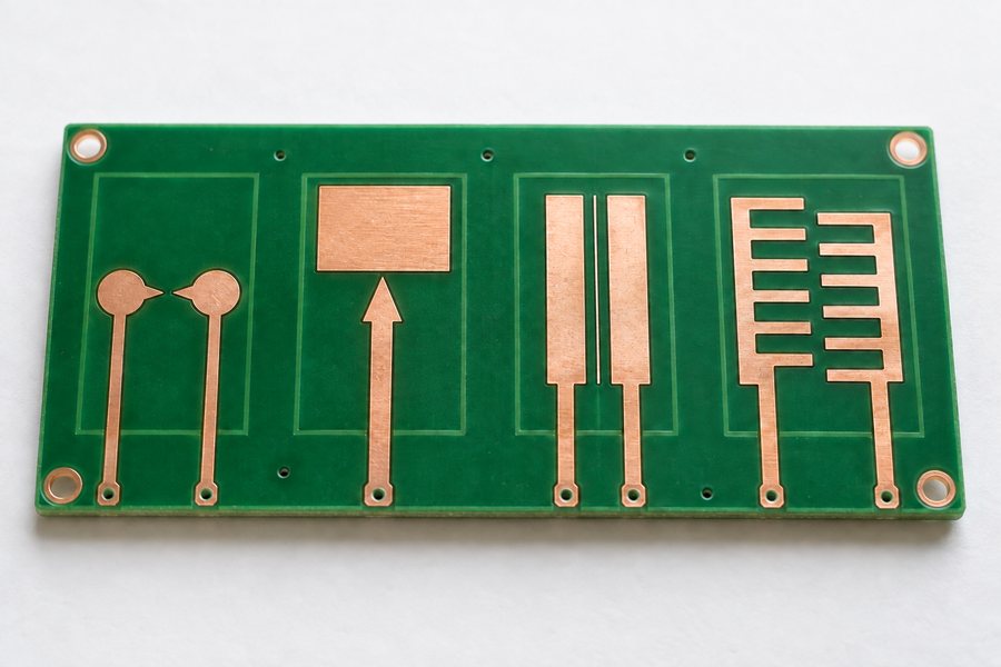
| Geometry | Field Behavior | Manufacturing Sensitivity | When to Use |
| Point to point | Strong concentration at both tips | High; tip radius and erosion cause larger shifts | When a controlled arc location matters |
| Point to plane | Concentration at one tip | High at the pointed electrode | When a preferred initiation side is useful |
| Parallel edges | Field distributed along the edges | Moderate; edge width and etch still matter | When reproducibility matters more than one fixed arc point |
| Interdigitated teeth | Multiple local high-field regions | High; more edges collect process and contamination variation | Only when multiple initiation sites have been intentionally evaluated |
Select the geometry according to the required arc control and production stability, not just the smallest CAD distance. Sharp tips can favor a specific discharge point, but their finished radius is highly process-sensitive. Broader edges can be easier to reproduce, while allowing the arc to move. Repeated events can erode either shape and carbonize the board surface, so the first firing result does not establish long-term behavior.
How Should You Design a PCB Trace Spark Gap?
Design the spark gap as a controlled layout object, not as two trace ends that happen to be close. The fabrication data must make six physical requirements unambiguous.
- Finished copper-to-copper gap: Set the nominal value and allowed finished tolerance from the tested candidate range.
- Electrode tip geometry: Use tips or edges the PCB process can reproduce, then dimension their finished relationship.
- Copper width: Give the transient path enough width and keep the neck behind each electrode short.
- Mask opening: Expose the active copper after allowing for solder-mask registration tolerance.
- Surrounding clearance: Keep pads, vias, planes, board edges, and component terminals from becoming an easier arc path.
- Discharge connection: Dimension enough copper behind the return electrode to avoid a narrow or inductive bottleneck.
Wrong layout logic: connector, then a long signal trace, then the spark gap. In this order, the ESD current has already traveled beside or through the protected circuit before reaching the diversion point.
Better layout logic: connector, then the spark gap, then the protected circuit. The gap intercepts the entry before the signal branches into the board, while its return electrode connects through a short, wide path to the chosen transient return.
Document the feature in the schematic, footprint, fabrication drawing, and assembly notes. This prevents automated copper cleanup, mask editing, or conformal coating from changing its function.
Where Should You Place a PCB Spark Gap for ESD Protection?
Place the spark gap as close as practical to the ESD entry point and before the transient reaches sensitive circuitry. Make the placement decision by answering three layout questions.
Where does ESD enter? Identify the connector pin, exposed metal, cable, switch, test point, or user-accessible contact that receives the event. Put the gap before that conductor reaches its first sensitive branch.
Where should the current leave? Select chassis, shield, or a dedicated transient return and verify continuity through connector shells, fasteners, seams, and return bonds. The gap should not discharge into an ordinary signal-ground path simply because it is nearby.
What must stay outside the path? Keep clocks, reset lines, analog inputs, high-impedance nodes, communication traces, and their reference copper away from both the arc site and the return route. Inspect every layer for coupling into planes or traces below the feature.
Texas Instruments shows a 0.2 mm connector-side pattern in one battery-gauge application. That is useful evidence that etched gaps can be integrated near an interface, but 0.2 mm is not a universal PCB spark gap distance. The referenced circuit, environment, geometry, current return, and validation target must be comparable before any pattern is reused.
How Do PCB Manufacturing Tolerances Affect the Final Gap Distance?
The CAD gap is not the finished gap, and minimum trace/space capability does not guarantee repeatable spark-gap geometry. Etching changes the copper edges, an ideal point becomes a finished radius, and mask registration changes the exposed path. Convert those effects into explicit order requirements.
The fabrication drawing should state:
- Nominal finished gap measured copper to copper, not only the CAD distance.
- Allowed gap tolerance and the sampling or inspection method used to verify it.
- Electrode geometry including the dimensioned tip or facing-edge profile.
- Solder-mask opening with registration allowance around the active electrodes.
- Copper weight used by the tested design because etching behavior changes with copper thickness.
- Surface finish matching the electrically validated samples.
- Conformal-coating keepout when the design depends on an exposed-air path.
- Inspection requirement covering the finished gap, electrode profile, mask opening, and keepout.
- Intentional-feature note so CAM review does not close, widen, or remove the unusual spacing.
For a manufacturing review, also provide the Gerber or ODB++ files and the target ESD or functional requirement. Ask the PCB manufacturer to confirm which dimensions can be controlled and measured as finished features. Then measure boards from production-intent panels before electrical testing. Release criteria should cover the resulting distribution, not one ideal coupon.
When Should You Combine a PCB Spark Gap With a TVS Diode or GDT?
Add a TVS diode or GDT when the PCB spark gap alone cannot hold the protected node within its voltage limit, absorb the required energy, or survive the expected number of events. Device choice starts with clamping accuracy, event energy, repetition, capacitance, and the maximum voltage the downstream circuit can tolerate.
| Protection Device | Clamping Characteristic | Main Limitation | Best Use Case |
| PCB spark gap | Coarse, variable sparkover | Wide variation, erosion, contamination sensitivity | Low-loading diversion at an entry point |
| TVS diode | Specified dynamic clamp | Capacitance, leakage, finite pulse rating | Holding a sensitive node within a voltage range |
| Gas discharge tube | Higher-voltage crowbar action | Turn-on delay, follow current, package size | Higher-energy surge diversion |
| Series impedance | Reduces current between stages | Can affect signal or power delivery | Coordinating a coarse and a precise clamp |
The roles are distinct: the PCB spark gap provides coarse diversion, a TVS controls residual voltage more tightly, a GDT handles higher-energy diversion, and series impedance coordinates current between stages. One possible sequence places the connector first, followed by a PCB spark gap or GDT, series impedance, a TVS diode, and the protected IC. Verify the turn-on order, protected-node voltage, current sharing, component stress, and function after repeated events.
How Should You Validate a PCB Spark Gap Before Production?
Validate the finished board under a defined equipment-level test and inspect both electrical behavior and physical damage. IEC 61000-4-2 establishes a common basis for equipment ESD immunity testing, but the applicable severity and acceptance criteria still come from the product requirement.

Step 1: Measure. Record the finished gap, tip profile, mask opening, finish, and residue condition on production-intent samples.
Step 2: Test. Apply the defined ESD method, levels, polarities, points, operating states, and pulse count at relevant environmental corners.
Step 3: Observe the discharge path. Confirm that the intended gap fires before a component lead, connector edge, enclosure seam, or unrelated copper feature.
Step 4: Monitor the circuit. Capture protected-node voltage and record resets, corruption, latch-up, communication errors, damage, and recovery.
Step 5: Inspect repeated-event damage. Look for tip erosion, carbon tracks, coating damage, firing drift, and accumulated functional degradation before making the release decision.
A candidate passes only when:
- the intended gap fires before another PCB or enclosure feature;
- no unintended flashover occurs;
- the protected circuit remains functional during and after the required test;
- the measured transient at the protected node stays within the circuit’s accepted limit;
- repeated pulses do not create progressive carbon tracking or unacceptable firing drift; and
- production-intent boards show consistent behavior across the allowed finished-gap range.
Keep the release record tied to board revision, fabrication lot, measured geometry, firmware state, test setup, and acceptance limits. A visible spark alone is not a pass.
What Common PCB Spark Gap Design Mistakes Should You Avoid?
Most failures come from treating the gap as an isolated CAD dimension instead of a manufactured discharge path. These six checks catch the highest-value errors before compliance testing.
- Copying a published gap value: The same distance can fire differently when electrode shape, finish, altitude, return path, or test setup changes.
- Using the ESD generator setting as Vgap: Other protection elements and coupling paths can change the voltage that appears across the electrodes.
- Putting the gap after a long signal trace: ESD current has already entered the circuit before it reaches the diversion point.
- Leaving an easier unintended path: A nearby pad, via, plane, connector shell, component lead, or board edge may flash over first.
- Using a poor return path: Shared return impedance can raise the local reference voltage even when the intended gap fires.
- Treating the gap as safety clearance: A spark gap is intended to break down, while safety spacing is intended to prevent breakdown.
FAQs About PCB Spark Gaps
Q1: Can a PCB spark gap protect USB, CAN, or RS-485 interfaces?
A1: It can provide coarse diversion at the connector, but it is usually only one part of the protection network. A suitable TVS diode may still be needed to control residual voltage. For high-speed interfaces, verify the protection network’s capacitance, signal integrity, protected-node voltage, and recovery after repeated ESD events.
Q2: Why does a PCB spark gap sometimes fail to fire during ESD testing?
A2: Check the finished gap first, then confirm that enough transient voltage actually appears across the electrodes. Rounded tips, solder mask, coating, pressure, surface condition, or another protection device can change the discharge path. Measure the waveform and inspect the exposed geometry before reducing the distance.
Q3: Can you simulate a PCB spark gap before building the PCB?
A3: Field simulation can compare electrode shapes and electric-field concentration, while circuit simulation can examine voltage division and protection coordination. Neither method fully predicts statistical air breakdown, contamination, tip erosion, or finished-board tolerance. Use simulation to narrow the candidate range, then establish release values on measured hardware.
Q4: Does copper weight affect PCB spark gap performance?
A4: Yes. Copper thickness affects etching and can change the finished tip profile, edge shape, and copper-to-copper distance. If copper weight changes between prototype and production, ask the manufacturer to confirm the new finished geometry and repeat the relevant electrical tests before treating the earlier result as valid.
Q5: Should a PCB spark gap use ENIG, HASL, or another surface finish?
A5: No single finish is automatically best for every spark gap. The finish can alter the exposed surface, edge profile, oxidation behavior, and local repeatability. Keep the production finish consistent with the tested samples, or requalify the gap when a process change alters the finished electrodes.
Q6: Can a PCB spark gap be placed on an inner PCB layer?
A6: Not when the intended mechanism is an exposed-air discharge. An inner-layer gap is surrounded by solid dielectric and behaves differently from an external exposed structure. Keep a conventional PCB spark gap on an exposed surface unless a separately engineered internal structure has its own electrical and reliability validation.
Q7: Can multiple PCB spark gaps be used on one connector?
A7: Yes, when several exposed conductors can receive ESD independently. Each gap needs a controlled return path and enough separation from adjacent signals, metalwork, and other gaps. Test the complete connector arrangement because one firing channel can couple voltage or current into its neighbors.
Q8: Does PCB thickness affect spark gap behavior?
A8: Board thickness usually has less direct influence than electrode spacing and shape, but it can matter near board edges, internal planes, chassis structures, or mounting hardware. Review the three-dimensional path whenever a discharge could travel around an edge or couple into nearby conductive layers.
Q9: Should a PCB spark gap appear in the schematic and BOM?
A9: Document it clearly even though it normally does not require a purchased BOM item. A custom schematic symbol, controlled footprint, and fabrication note can identify the two nets, finished geometry, mask opening, and test requirement. This reduces the chance of removal during layout or CAM review.
Q10: When should you remove a PCB spark gap instead of optimizing it?
A10: Choose another protection method when firing variation, repeated-arcing damage, or manufacturing distribution cannot meet the circuit requirement. A TVS diode, GDT, enclosure-level diversion, or redesigned current path may provide a more reliable result. The release decision should follow measured protected-node performance rather than attachment to one layout concept.
Conclusion
A PCB spark gap cannot be selected from voltage alone. Identify the ESD entry and discharge return, estimate a candidate distance, choose reproducible electrodes, convert them into finished-board dimensions, and place the diversion before the protected circuit. Coordinate a TVS diode or GDT when the residual voltage or event energy requires it. Release the design only after production-intent boards meet the defined electrical and physical acceptance criteria.
For a manufacturability review from EBest Circuit, send the Gerber or ODB++ files, gap dimensions and tolerance, copper weight, surface finish, solder-mask and coating requirements, plus the target ESD test to sales@bestpcbs.com. Those inputs allow the team to review whether the intended geometry can be built and inspected before quotation or production.