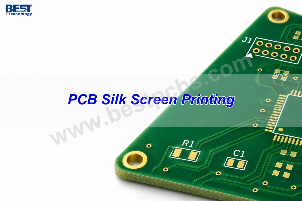
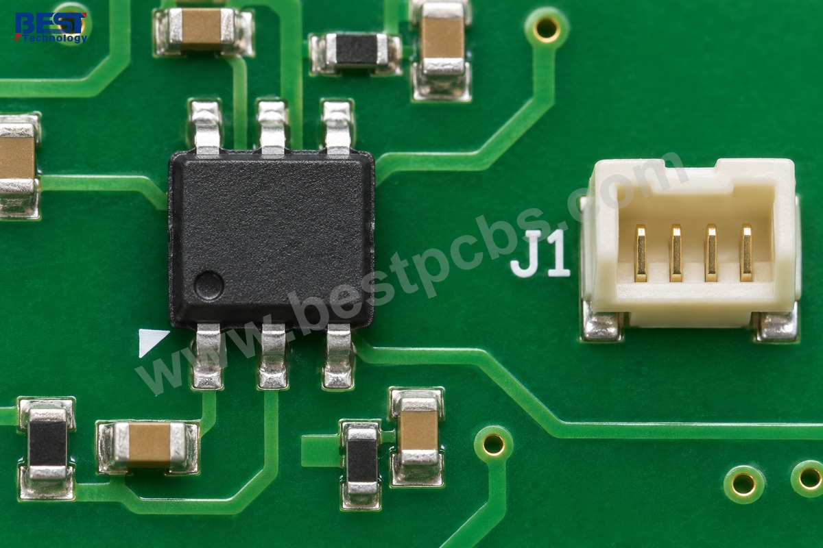
PCB Silk Screen Printing puts visible markings on a circuit board: reference designators such as R12, connector labels such as J1, and symbols that show polarity or pin 1. In traditional screen printing, a squeegee pushes ink through a patterned mesh onto the board. A factory may instead use direct inkjet printing, even when the design files call the layer “silkscreen.” In either case, the printed legend starts with your artwork. At EBest Circuit, we review that artwork during PCB design review, where a label can still be moved clear of a solder opening or a part that would cover it.
Key Takeaways
- Silkscreen identifies parts and connections. Solder mask protects the board and leaves openings where pads need to be exposed.
- A mesh screen transfers the pattern with a squeegee. Direct inkjet prints the same type of legend without a physical screen.
- Export the top and bottom legend layers separately. Check them against the solder-mask openings in a Gerber viewer.
- Move a critical mark away from a pad rather than relying on clipping. A missing stroke can turn a readable label into the wrong one.
- Inspect the bare board for missing, shifted, or smeared print. Check the assembled board for labels hidden by parts or hardware.
PCB Silkscreen vs Solder Mask: What Does Each Layer Do?
Silkscreen tells you what is on the board; solder mask covers the areas that should be protected. On a typical green board with white markings, the green layer is the mask and the white characters are the legend. The copper beneath the mask is a separate layer.
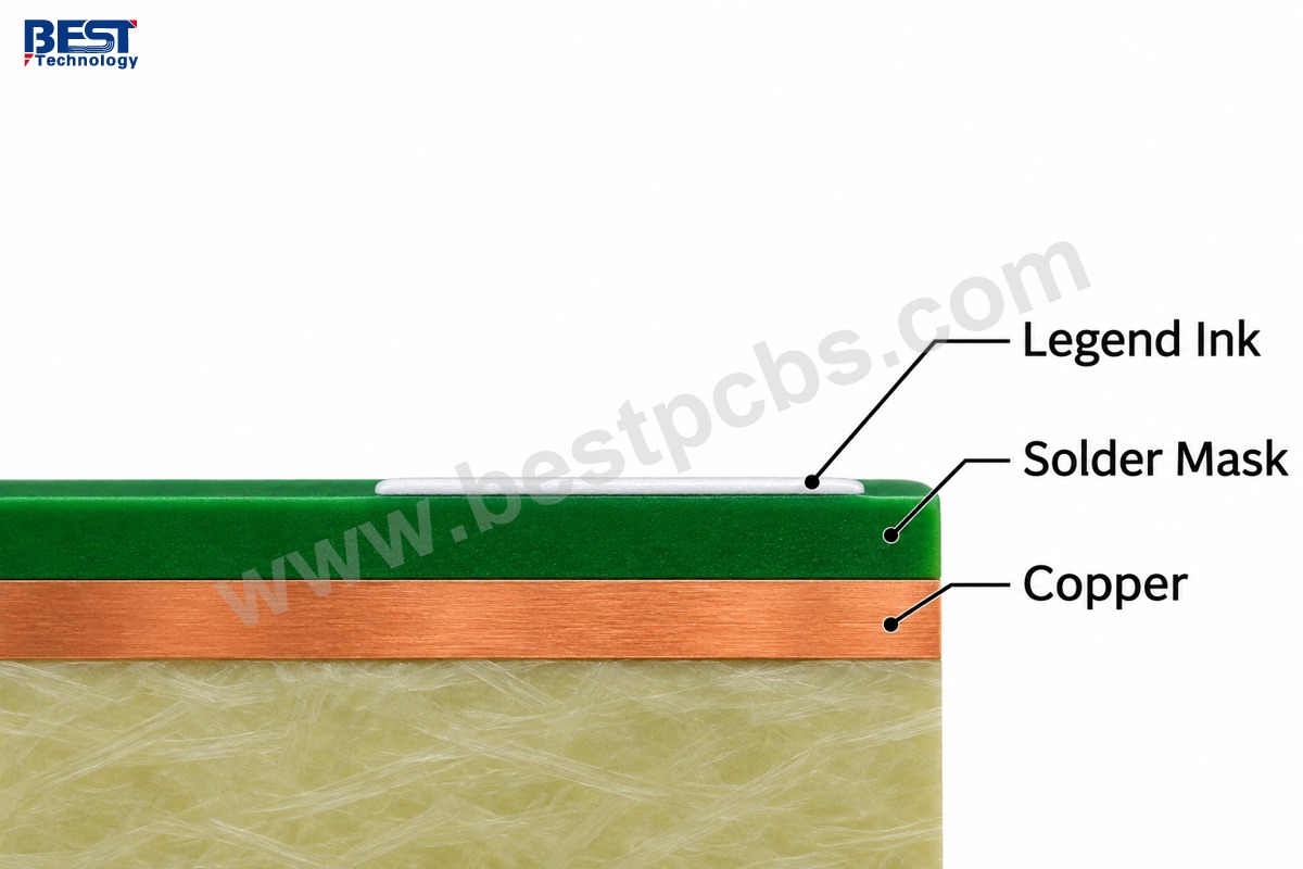
Different PCB silkscreen symbols serve different readers. An assembler uses a pin 1 marker to orient a device. A technician uses a test-point label to find a signal. A component outline helps with placement, but the outline itself does not tell you which way a polarized part goes.
How Does PCB Silk Screen Printing Work?
The fabricator aligns a patterned screen over the panel, transfers the legend with a squeegee, then cures and checks the print. The screen defines where ink can pass through the mesh. The operator holds the panel in register so the markings line up with the pads and outline.
- Prepare the pattern. Review the legend file against the mask and board outline before making the screen.
- Align and print. Position the panel beneath the screen and draw the squeegee across it. Ink passes through the open areas to form the markings.
- Cure and inspect. Cure the legend using the method specified for that ink. Check print position, missing strokes, and stray ink.
Direct inkjet uses a digital file to place the markings without making a mesh screen. That avoids remaking the screen when the artwork changes. Both methods still need readable artwork and enough clearance from exposed pads. For more on the production sequence, see our PCB screen printing process.
Which Gerber Layers Should You Send?
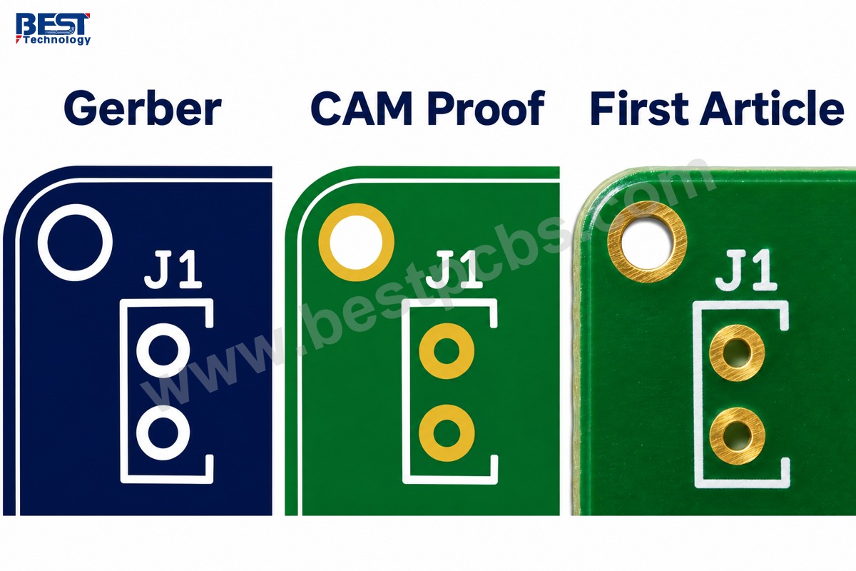
Send a separate legend layer for each printed side, together with the corresponding solder-mask layer and the rest of the fabrication files. In KiCad, the legend layers are F.Silkscreen and B.Silkscreen. Text drawn only on a fabrication drawing layer does not appear in the legend Gerber.
Open the exported files rather than checking only the CAD view. Overlay the legend and solder mask for each side, then check the bottom lettering from the bottom of the board. Keep the same origin across the files and avoid flipping a single layer by hand. If trimming would make a connector label ambiguous, flag it on the drawing before the fabricator prepares the production artwork.
Why Does PCB Silk Screen Printing Lose Part of a Letter?
In PCB silk screen printing, a legend can lose strokes when the artwork crosses a solder-mask opening or when the characters are too fine for the selected process. A fabricator may trim the print back from openings so ink does not land on a solderable surface. If a trim cuts into the vertical stroke of the “1” in J1, the text can still be present but no longer readable.
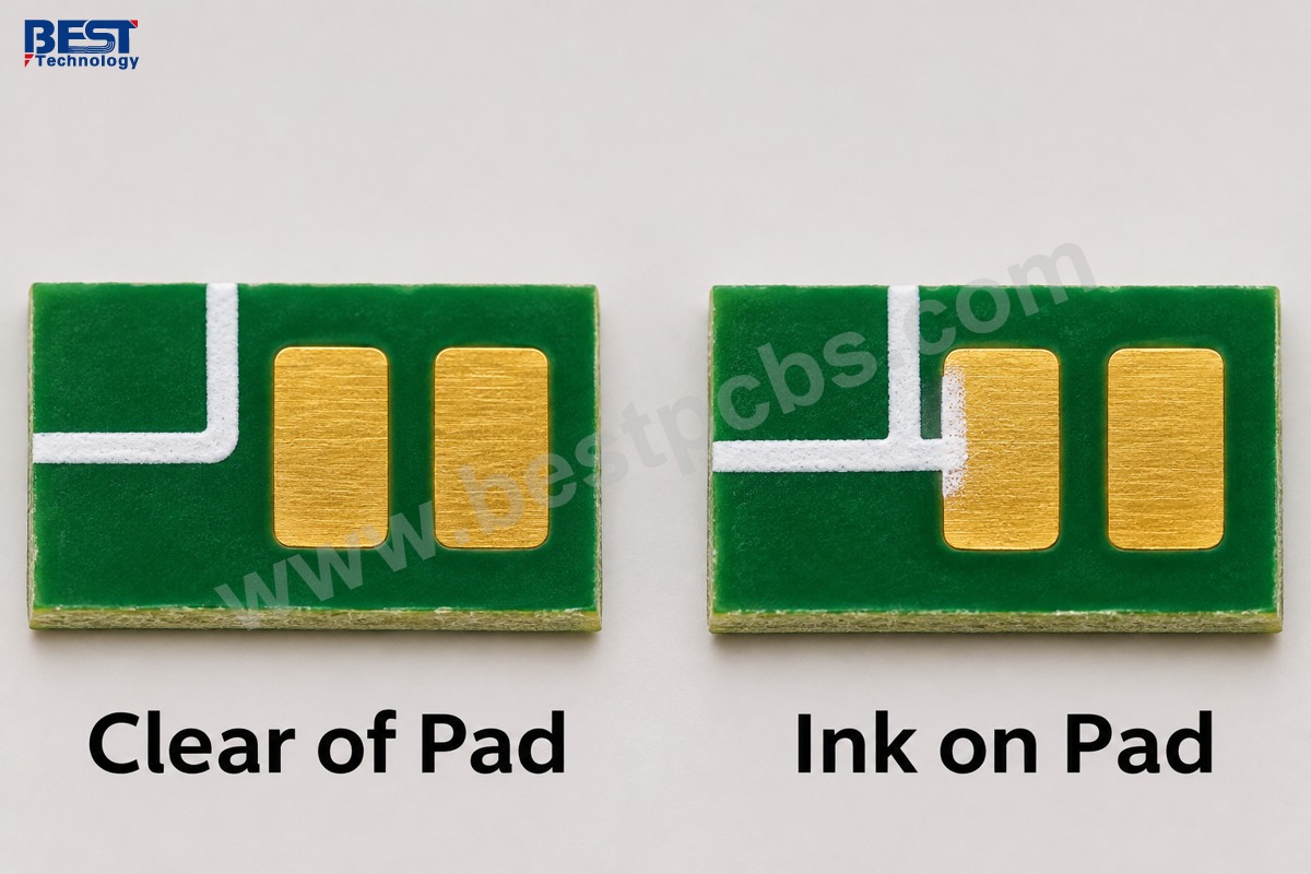
Check stroke width as well as text height. Two fonts at the same height can print differently if one has thinner strokes or tighter spacing. For a mark between connector pads, moving it to open board space usually works better than making it smaller. Use the PCB silkscreen guidelines when laying out the legend, then confirm the limits for your board and printing method.
How Do You Inspect PCB Silk Screen Printing?
Check the bare board for print quality and the populated board for visibility. A correctly printed J1 label can still disappear beneath the connector housing after PCB assembly.
| What you see | What to check first |
|---|---|
| One letter or stroke is missing | Compare the exported Gerber with the production artwork around the nearest mask opening. |
| Several labels shift in the same direction | Compare their positions to the pads and check print registration. |
| Small characters merge or smear | Check stroke width and character spacing, then inspect the print. |
| A label disappears after assembly | Check the connector, shield, or fastener outline in the assembled view. |
FAQ About PCB Silk Screen Printing
Is white the only silkscreen color?
No. The fabricator’s PCB silk screen printing process determines which colors are available. For silkscreen PCB material, specify a legend color that contrasts with the solder mask. White on dark green and black on white are common combinations.
Can a board have silkscreen on both sides?
Yes. Supply artwork for both sides and ask the fabricator to print both. Check text orientation separately on each side.
Does an SMT stencil print the silkscreen?
No. An SMT stencil deposits solder paste on pads during assembly. A patterned screen for PCB legend printing transfers marking ink during fabrication.
Can I put a QR code in the silkscreen?
Yes, if the selected printing process can reproduce it at the required size. Check contrast, the clear margin around the code, and scanning on an actual sample. If you need a different code on every board, discuss variable-data marking with the fabricator.
Can silkscreen be added to a board without solder mask?
Yes, if the fabricator supports printing on the exposed laminate. The surface and ink must be compatible, and markings should still stay off solderable pads.
Review the Legend Before Fabrication
Flag any pin 1 mark, terminal label, or traceability code that needs to stay exactly where you placed it. Send the legend and mask layers to sales@bestpcbs.com so we can review the artwork with your PCB fabrication requirements.