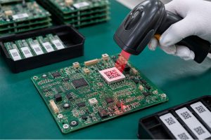
QR code marking on copper works when a reader can distinguish the code’s small squares from the surrounding surface. The challenge is keeping that contrast through finishing, cleaning, and assembly. On a PCB, the marking process must also preserve the copper needed for the circuit.
A useful code starts with three decisions: what it must identify, where it will be placed, and when it must be scanned. This guide explains how those choices affect the marking method, code size, readability, and the production records a PCB or PCBA buyer can retrieve.
What Is QR Code Marking on Copper?
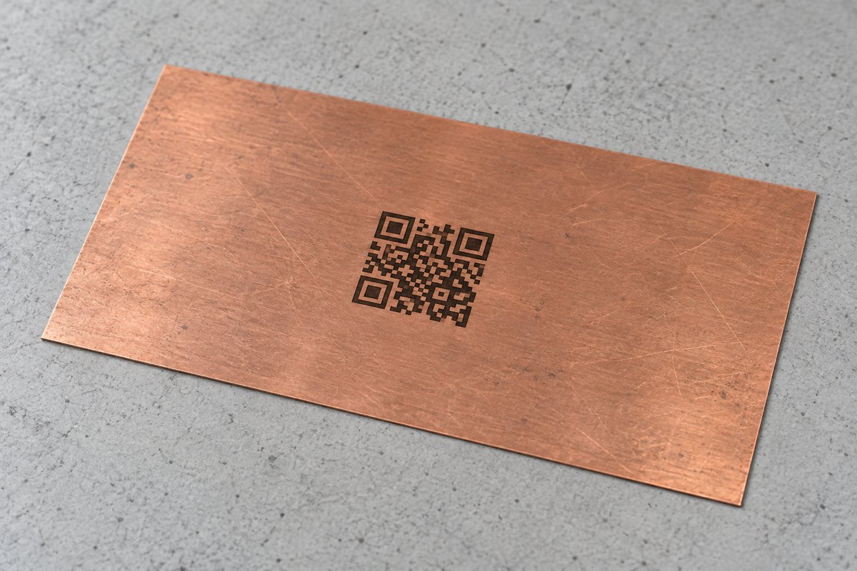
QR code marking on copper creates a machine-readable pattern on a copper surface. Direct laser marking changes the surface’s appearance or texture; engraving removes material to form the pattern. A PCB can also carry a QR pattern formed in its copper artwork.
Each small square in a QR code is called a module. The reader must distinguish the two module states, recognize the corner patterns, and see a clear border around the symbol. That border is the quiet zone. On reflective copper, the contrast seen by the reader can change when the lighting or viewing angle changes.
The code’s purpose determines its data. A part number identifies a product type. A batch code identifies a production group. A unique serial number identifies an individual board or part. For traceability, that identifier can retrieve manufacturing records without storing all those records inside the code.
Which Methods Work for QR Code Marking on Copper?
Choose the method according to the surface being marked and whether the code must change from unit to unit. Several approaches can create a copper-related pattern, but they do not perform the same operation.
| Method | Suitable starting point | Important limitation |
|---|---|---|
| Direct laser marking | A variable identifier on a copper surface | Contrast must be achieved within the part’s allowable surface change |
| Mechanical engraving | A robust copper part that can tolerate material removal | Not a default method for thin PCB copper foil |
| Patterned PCB copper | A fixed identifier included in board artwork | Repeated artwork repeats the identifier; it does not automatically serialize boards |
| Selective solder mask removal | A pattern created by exposing copper beneath the mask | The process acts on the coating and must protect the underlying board |
A fixed code and an individual serial number solve different problems. If every board only needs to identify the product model, a repeated artwork code may be sufficient. If each board needs its own test history, the production process must assign and apply a distinct identifier.
Also distinguish direct copper marking from exposing copper through solder mask. They may look similar in a photograph, but their process settings and failure modes differ.
Which Laser Works Best for Marking QR Codes on Copper?
A pulsed fiber laser is one established option for direct copper marking. Green and UV marking systems are additional candidates where the material response or fine-feature requirements call for a different wavelength. The best choice is the one that produces readable modules while staying within the part’s allowable surface change.
Pulsed infrared fiber lasers: Suitable settings can produce contrast on copper, but reflective copper requires careful control of the interaction. Pulse duration, focus, scan speed, and repeated passes affect the result. Raising average power alone does not resolve those variables.
Green and UV marking lasers: These offer different interactions with the material and can be evaluated for non-ferrous metals and fine marking tasks. A shorter wavelength does not automatically make a process safe for PCB foil. The actual spot size, pulse characteristics, and material stack still matter.
For a PCB, first distinguish direct copper marking from removing solder mask. The first changes the metal; the second should remove the intended coating while protecting the copper below. A successful demonstration on a thick copper part does not qualify either process for a finished board.
Compare samples at the intended code size and production speed. Reject a process that gives strong contrast but damages functional copper, or preserves the board but produces inconsistent scans. This gives the equipment choice a measurable target: readable codes on acceptable parts.
Why Won’t a QR Code on Copper Scan?
The most useful first question is whether the failure changes when you move the light or the reader. If it does, investigate reflections before changing the marking depth. If it does not, inspect the code geometry and reader setup.
| Symptom | What it suggests | What to check first |
|---|---|---|
| Reads only when tilted | Angle-dependent contrast or glare | Lighting arrangement and reader orientation |
| Small squares merge or vanish | Inadequate feature definition | Module edges, focus, and marking resolution |
| Reader cannot locate the symbol | Obstructed border or damaged corner patterns | Quiet zone and the three finder patterns |
| Reads before processing but fails afterward | Surface change or contamination | The operation between the last successful scan and the failure |
Confirm that QR decoding is enabled on the reader. Check its working distance and field of view: a code can be sharply marked yet occupy too few image pixels to decode reliably.
Increasing laser power is not a general fix. It may change the surface or spread feature edges without solving glare. Likewise, QR error correction can tolerate some damage, but it cannot compensate for every loss of contrast or missing feature.
How Small Can a QR Code on Copper Be?
Calculate the required area from the encoded data and module size, including the quiet zone. Do not choose a marking area from the visible pattern alone.
A standard QR code requires a quiet zone four modules wide on each side:
Overall side length = (modules per side + 8) × module width
For a Version 1 code with 21 modules per side, an illustrative module width of 0.20 mm gives:
(21 + 8) × 0.20 mm = 5.8 mm per side, including the quiet zone.
This calculation defines the reserved area. It does not establish 0.20 mm as a suitable module size for every copper marking process or reader.
Consider a hypothetical board identifier, B260914001. A code containing that short identifier can retrieve a larger production record from a database. Encoding the full record instead may require more modules and therefore more space at the same module width. Confirm the actual data capacity and error correction setting before finalizing the layout.
If space is limited, shorten unnecessary data before shrinking the modules. Then confirm that the marking process can reproduce the resulting pattern and the intended reader can resolve it.
Should You Mark Copper Before or After Surface Finishing?
Marking before finishing exposes the pattern to later surface changes. Marking afterward gives you the final surface to work with, but may disturb the finish itself. Choose the sequence around both the finish’s function and the first required scan point.
Before finishing: Plating or coating can cover the marked surface or change how it reflects light. A contrast pattern that reads clearly on bare copper may look different afterward. If the mark relies on a particular surface color or texture, evaluate it after the complete finishing sequence.
After finishing: The code can be optimized for the surface the reader will actually see. However, engraving or removing that finish may expose underlying material or change a functional area. A code should not compromise a surface needed for protection, soldering, or electrical contact.
For example, a code required only during final inspection may be applied later than one needed to track the board through earlier production steps. If early processing would obscure the permanent mark, an earlier identifier must remain linked to the final board identifier.
For a PCB order, specify the finish, marking location, and when scanning must begin. A sample that scans before finishing answers a different question from a sample that scans after finishing and assembly.
When Can PCB Laser Marking Damage the Copper Layer?
PCB laser marking can cause damage when it removes or alters copper that the circuit needs. Excessive energy or repeated passes may thin a conductor, change a pad surface, or affect nearby mask and laminate.
A readable code is not proof that the board remains electrically acceptable. A deep mark may improve one aspect of contrast while reducing the copper cross-section. On a functional pad, surface changes may also interfere with its intended use.
Separate the permitted marking area from functional pads and traces during layout and manufacturing review. Do not assume that a visually empty copper area is electrically unimportant: a copper pour may be serving as a plane or current path.
When the process is intended to remove solder mask, review whether it stops at the intended layer. When it is intended to modify copper, define what surface change the design can tolerate. Relevant inspection or electrical checks should follow that mechanism, rather than treating every laser mark as the same risk.
Should You Place a QR Code on PCB Copper or Solder Mask?
Choose a location that remains accessible at the actual scan points. The board’s assembled condition can matter more than how convenient the location looks in the bare-board drawing.
Consider a solder mask area when it provides useful contrast and separates the marking operation from exposed functional copper. Its suitability still depends on mask color, thickness, and the marking process.
Consider a copper area when the identification requirement calls for it and the design provides a suitable region. Include the final finish and reflected light in the readability assessment.
Check for components, shields, connectors, and later coatings that could cover or obscure the symbol.
A panel-rail code can identify a panel during fabrication, but the rail is later removed. If individual boards need traceability afterward, map them to their own identifiers before that link disappears. Keeping a code visible and keeping its history connected are both part of placement planning.
How Do You Verify a QR Code on Copper After Processing?
Check readability, decoded data, and the marked product separately. Each answers a different question.
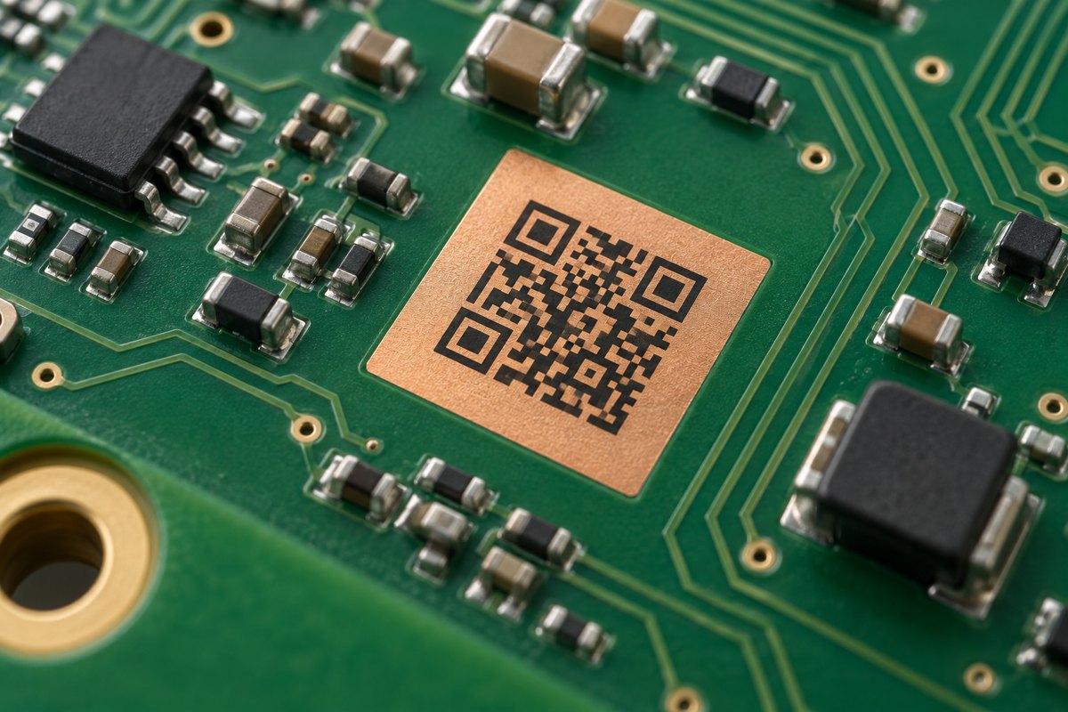
Check the physical symbol. Inspect module edges, corner patterns, the quiet zone, and visible surface damage. Read the code with the intended reader at the working distance and lighting used in production. Include relevant finishing, cleaning, assembly, and coating steps in the evaluation.
Check the quality requirement. A successful phone scan demonstrates that one device decoded the symbol under those conditions. It does not establish a specified quality grade. Where grading is required, agree on the applicable verification method and lighting. ISO/IEC 15415 addresses two-dimensional symbol quality, while ISO/IEC 29158 addresses direct part marking quality. Select the applicable method and lighting for the actual marking application; do not assign a grade from a casual scan.
Check the identity and product. In the hypothetical example, B260914001 should retrieve the intended board’s record. A second board accidentally carrying that same identifier might scan perfectly while undermining individual traceability. Check for duplicate or incorrect values, and complete the physical or electrical checks required by the marking process.
How Can PCB Laser Marking Support PCB and PCBA Traceability?
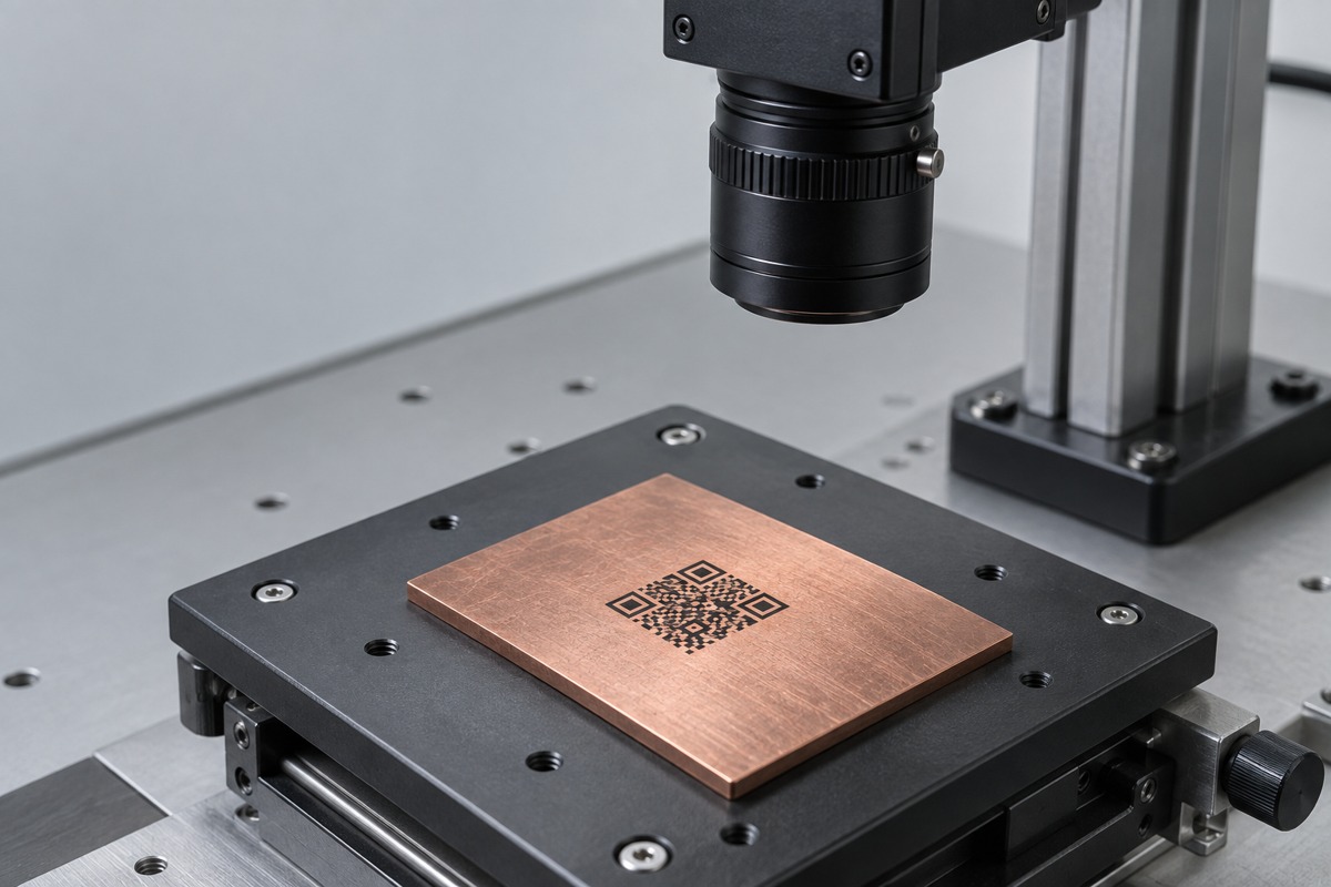
PCB laser marking gives production records a physical reference on the board. Its value to a buyer is being able to connect a delivered assembly or field return to the relevant manufacturing history.
Batch identification helps narrow an investigation. If a material lot or production batch is affected, linked records can help identify which boards belong to that group. The usefulness of the search depends on the records captured during production.
Individual identification supports board-specific history. A unique code can connect one assembly to its inspection results, test results, and rework events. For the example B260914001, the database holds those records; the symbol supplies the identifier used to find them.
PCB-to-PCBA handoff preserves continuity. The assembler needs to retain the fabricator’s identifier or map it to the assembly identifier. Otherwise, PCB fabrication history and assembly records may remain separate even though both operations use codes.
A manufacturing execution system, or MES, can manage these associations. The marker applies the identifier, the reader checks it, and the production system connects it to records. The QR code does not collect manufacturing data by itself; each relevant operation must record its results against the correct identifier. Smaller operations can use controlled records without a full MES, as long as each code retrieves the correct history.
For your next PCB or PCBA order, define what you need to retrieve when a board is scanned: a production batch, an individual test result, or a repair history. Then specify whether the code must remain accessible after assembly. These decisions help avoid an obscured code or a readable identifier that leads to incomplete records.
FAQs about QR code marking on copper
Can a QR code be marked directly on copper?
Yes. Laser marking can create a readable pattern directly on copper. The process must produce sufficient contrast without exceeding the surface change the part can tolerate. Thin PCB copper needs a different assessment from a solid copper part.
What is the minimum size for a QR code on copper?
There is no universal minimum. It depends on the encoded data, module size, marking accuracy, and reader resolution. Include a quiet zone four modules wide on every side when calculating the required area.
Will a copper QR code remain readable after surface finishing?
Not automatically. Plating or coating can change its appearance and contrast. Evaluate readability after the planned finishing sequence, using the intended reader and lighting conditions.
Does a QR code need an MES to support traceability?
No. Controlled records can support traceability without a full MES. Each identifier must remain linked to the correct production history. An MES can manage those associations, but the code itself does not collect production data.
Should every PCB have a different QR code?
Use a unique identifier when you need individual test results or rework history. A shared batch code can support batch-level tracking, while a fixed product code identifies the model rather than an individual board.
Discuss your PCB fabrication or assembly requirements with EBest Circuit (Best Technology) at sales@bestpcbs.com. Send your Gerber files and quantity, plus the BOM for assembly work, and describe the identification you need. State whether copper marking is mandatory or another board location is acceptable, so the proposed marking approach can be assessed as part of the order. You do not need to choose a laser before making an enquiry. Discuss QR code marking on copper requirements with your enquiry.