Use a copper Invar copper PCB when controlling how much the board expands across its surface matters more than simply maximizing heat flow through its thickness. The copper faces spread heat along the plane and the Invar center restrains expansion. But the same center can limit heat flow across the clad. Treat board expansion and the vertical thermal path as two separate design checks.
Consider a multilayer board carrying a ceramic package near a chassis heat sink. If the main concern is relative movement at the package joints, a copper/Invar/copper plane is worth screening. If the design is failing its junction-temperature budget, find the layer or interface that consumes that budget before changing the core.
What Is a Copper Invar Copper PCB?
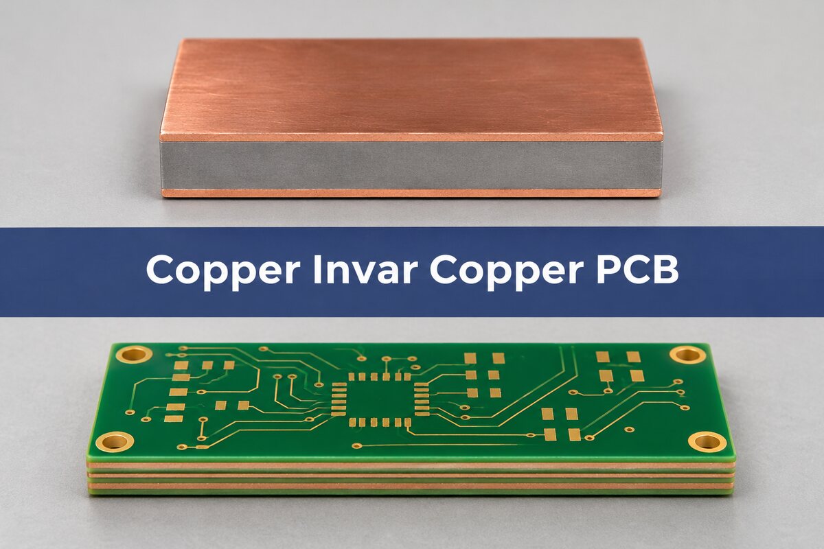
It is a PCB that incorporates a bonded metal composite with copper on both sides of a low-expansion iron–nickel alloy. The material is abbreviated CIC. It can be used as a plane within a multilayer stack or as part of a separately specified metal-backed construction. The supplier’s EMS electronic-materials sheet shows these roles. CIC by itself is conductive; any required electrical isolation comes from the surrounding construction, not from the Invar center.
The copper faces and center are bonded, so the layers do not expand freely and independently in the plane. The result depends on thickness fraction, mechanical properties and temperature. More importantly, a CIC sheet is only one layer in a PCB. Glass reinforcement, resin, patterned copper and the placement of the clad all affect the finished board.
Copper Invar Copper Cladding: What the Ratios Mean
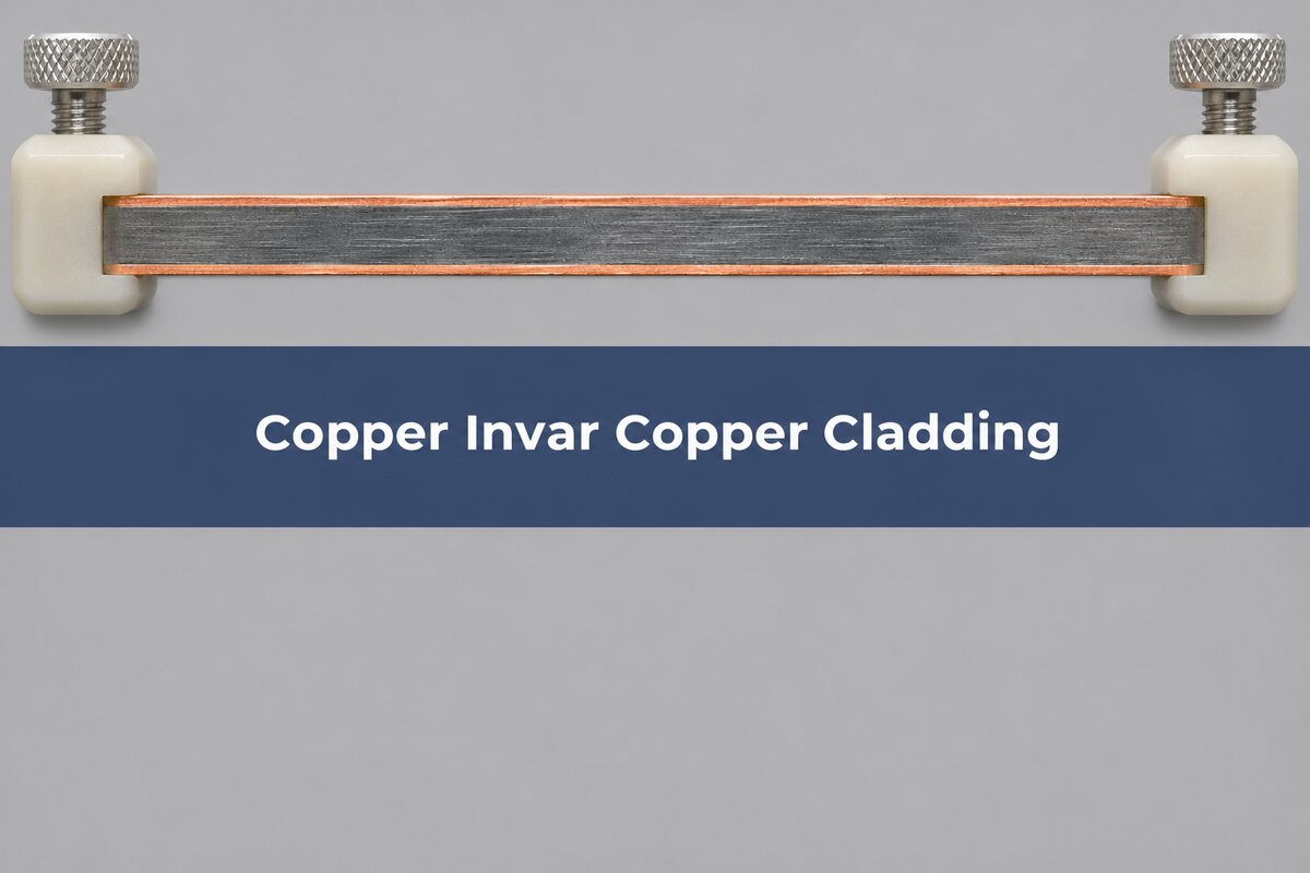
A ratio such as 12.5/75/12.5 describes the proportions of copper, Invar and copper, in that order. It is not a copper weight or a plating specification. Compare the ratio with the overall clad thickness, the resulting foil thickness on each side, and the material condition. Equal copper faces help keep the clad symmetric; they do not make an asymmetric PCB stackup flat.
| Clad property | 12.5/75/12.5 | 20/60/20 |
| Copper fractions | 12.5% per face | 20% per face |
| X/Y conductivity at 20 °C | 110 W/(m·K) | 167 W/(m·K) |
| Z conductivity at 20 °C | 19 W/(m·K) | 20 W/(m·K) |
| Reported linear CTE, −55 to +125 °C | 2.4–5.6 ppm/K | 2.54–5.08 ppm/K |
These are information-only values from Schlenk’s CIC 12.5 sheet and CIC 20 sheet, both rev. 1/2018. They describe bare material, not a finished PCB or guaranteed tolerances. The reported linear CTE ranges overlap; they do not establish a winner for a particular board. EMS lists different CTE figures for its 20/60/20 product. Keep supplier, grade and reported conditions attached to the values instead of merging them into a universal range.
In Plane vs Through Plane Thermal Conductivity
Choose the conductivity value for the direction in which heat actually moves. For lateral heat spreading, the copper faces and center provide parallel paths. Through the thickness, heat crosses the layers in series. Higher X/Y conductivity therefore does not imply an equal improvement in Z conductivity. In the Schlenk comparison, the reported X/Y value rises by 57 W/(m·K), about 52% relative to 110, while the reported Z value rises by only 1 W/(m·K), about 5% relative to 19.
A teaching estimate makes the difference concrete. Assume a 0.10 mm clad sheet, a 5 × 5 mm effective heat-transfer area, uniform one-dimensional flow and the tabulated 20 °C Z values. For clad alone, R = t/(kzA): at 19 W/(m·K), R is about 0.211 K/W; at 20 W/(m·K), R is 0.200 K/W. The difference is about 0.011 K/W, or about 0.11 °C at 10 W in this model. That would not solve a several-degree system shortfall on its own. The real path also includes solder, insulating layers, interface resistance and heat spreading; model or measure those separately.
PCB Coefficient of Thermal Expansion: Match the Assembly
Match the finished board’s expansion to the parts it is attached to, not to the lowest number on a datasheet. For package joints, start with X and Y along the board, the package’s corresponding expansion data, and the temperature range experienced by the assembly. For plated barrels or vias, treat through-thickness expansion as a separate mechanism. A low X/Y value cannot establish through-hole reliability.
The coefficient of thermal expansion, or CTE, expresses how much a dimension changes per degree relative to its starting length. For example, 1 ppm/K means 1 µm of change per meter of initial length for a 1 K change when the coefficient is constant. A long package can therefore show more relative movement than a short one even when both use the same pair of materials.
Distinguish a clad-only CTE, a finished board CTE and the motion of a mounted assembly. A chassis that restrains the board can redistribute movement rather than remove it. Package geometry, joint stand-off and the actual temperature history affect whether a difference is important. For a wider view of plated interconnect and solder-joint failures, see the PCB thermal cycling test guide.
CTE Mismatch Equation: Estimate Relative Movement
Use a free-expansion estimate to decide whether a lower-CTE stack deserves a prototype. For constant effective CTEs over the relevant interval, the magnitude of the differential movement is approximately L × |αboard − αpackage| × ΔT, with CTE in 1/K. Choose L to match the location being evaluated; a complete span and a center-to-corner distance are not interchangeable.
Teaching example: assume a 30 mm span, a 100 K temperature change and a package CTE of 7 ppm/K. An assumed board CTE of 15 ppm/K gives 24 µm of free differential movement. An alternative finished board assumed at 8 ppm/K gives 3 µm, a reduction of 21 µm across the same span. These are assumed effective board values, not a prediction from the clad table. Use the result to prioritize a build and decide where to measure; it does not give solder stress, crack probability or cycles to failure. For a large interval with temperature-dependent behavior, use expansion curves for the relevant materials rather than extending one coefficient beyond its range.
Metal Core PCB Stackup: Place the Core With Intent
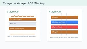
Define whether the clad is an internal plane or a metal base before assigning its electrical and thermal functions. An internal plane may be tied to a net or intentionally isolated. A metal base needs a defined path to the heat sink and a clearly identified insulation boundary. For drills passing near or through the metal, document clearances and which features are intended to connect. Agree with the fabricator on the proposed construction and inspection evidence before the stackup is released.
Copyable review worksheet: use this before releasing a drawing. Fill in the proposed and baseline constructions, then compare the evidence against your actual requirement. Close each unanswered item before committing to that material for production.
| Question | Record | Next decision |
| What expansion must be matched? | Contact span, axes, temperature range and package/board data. | Screen relative movement; measure the proposed build if only foil data is available. |
| Where does the heat leave? | Heat load, clad thickness, path area, dielectric and sink interface. | Check direction-specific values and the full thermal budget. |
| What does the released board need? | Clad location, net, hole clearances, layer symmetry and acceptance tests. | Request a complete stackup and verification plan, not approval of a material name. |
| Example decision | Source lists only X/Y heat flow while the sink is under the board. | Hold the thermal decision; obtain Z data and check the mounting interface. |
PCB Bow and Twist Measurement: Check the Finished Build
Check flatness on the board geometry you will actually assemble. Equal copper cladding on one material layer does not compensate for uneven copper distribution elsewhere, unequal dielectric sections or asymmetric placement of a stiff core. Document whether the sample was a panel or a singulated board, the support condition and when flatness was checked relative to thermal exposure.
When the procurement documentation invokes IPC-6012F (September 2023), use the applicable performance class and agreed procurement conditions under §§1.3.1–1.3.1.1 and check the applicable bow-and-twist requirement under §3.4.3. Confirm the invoked amendment or addendum and customer drawing before quoting a limit. A bow-and-twist measurement is not a replacement for assembled coplanarity or package strain evidence.
PCB Thermal Cycling Test: Read the Evidence
Qualify the candidate at the level of the risk. Bare-board X/Y expansion can explain the direction of a change, but solder-joint behavior requires a representative assembly. Compare the baseline and candidate at the same board revision and package design wherever possible. Request actual temperature endpoints, specimen identity and count, monitoring or inspection method, and the specified failure rule, not just the number of cycles.
If IPC-TM-650 2.4.41.2 Rev. A (May 2004) is specified for in-plane CTE, use its specimen rules in §3 to judge whether the report applies. The method describes strain-gage measurements on suitable specimens in X and Y; it is not a cycling life or acceptance criterion. A thin loose foil alone is not a substitute for the specified finished construction. When results are close, ask whether the lab’s repeatability and specimen spread are small enough to support a ranking.
Example report check: if the supplier provides a bare-board expansion plot but the decision is whether the package joints survive an assembly-level cycling requirement, use the plot for screening only. Hold the assembly release decision until representative joint evidence and the approved acceptance criterion are available.
Frequently Asked Questions
Does CIC mean the same thing as a copper coin?
No. CIC names a bonded copper–Invar–copper material; a coin describes a localized insert geometry. A solid copper coin addresses a local heat path. A CIC plane can change expansion across a larger board region. The two should be compared by their specific roles, not treated as interchangeable materials.
Can a CIC layer also carry current?
It is metallic, but electrical use needs an intentional net connection and verified conductor performance. Identify current entry and exit, which layers are connected, and whether the copper faces deliver the expected current path. Do not substitute the electrical properties of solid copper for the whole clad structure.
Is copper–molybdenum–copper a direct substitute?
No. Compare the actual grade, thickness, X/Y expansion over the required interval, Z conductivity and available fabrication route. A similar name does not establish equivalent drilling, bonding or electrical behavior. Treat any replacement as a stack change until the drawing and required verification have been reviewed.
Can I estimate the two copper-face thicknesses from the ratio?
For a uniform flat sheet, the nominal fractions can provide a first estimate. A 0.10 mm sheet at 12.5/75/12.5 gives 12.5 µm nominal copper on each face. Use the supplier’s guaranteed dimensions if the finished face thickness affects current, processing or drawing acceptance.
Does a low-CTE board eliminate the need for compliant joints?
No. The package, joints, board and mounting constraints work together. A closer expansion match may reduce one contributor to movement, but it does not validate joint geometry, assembly conditions or survival under the product’s load profile.
Is a single room-temperature conductivity value enough?
It can screen candidates if the test direction and material identity are known. If the actual temperature range, heat path or interfaces differ from the assumptions, use applicable properties and check the complete assembly. An information-only clad value is not a guaranteed product thermal resistance.
Should the prototype use the same clad supplier planned for production?
Keep material identity and condition traceable. If the source, temper, construction or thickness changes, agree on the evidence needed to show continued equivalence. Approval based on an unidentified coupon cannot be inherited by a different production stack.
Can a CIC board still use normal PCB data files?
Standard fabrication files can describe copper patterns and holes, but separately include a stackup drawing for material grade, clad orientation, metal connection or isolation, and acceptance requirements. Confirm the actual supplier data package before ordering.
Technical References
- EMS Cu/Invar/Cu electronic materials: construction and physical properties.
- Schlenk CIC 12.5 data sheet, rev. 1/2018, and CIC 20 data sheet, rev. 1/2018.
- IPC-6012F: rigid-board requirements and performance classifications; IPC-TM-650 2.4.41.2 Rev. A: strain-gage CTE test method.
Discuss Your PCB Stackup Before Release
Need a board that holds its dimensions without trapping heat? Before you lock the stackup, send Best Technology your layer drawing, package footprint, operating temperature range and heat-sink interface. Tell us where you need to control movement and how the board will be cooled. Request a stackup review and a quote for your build: sales@bestpcbs.com. Confirm CIC material availability and the verification scope with us before committing it to your design.