Wireless products depend on a stable RF path from the radio circuit to the antenna. An antenna PCB connector looks small, but it can affect signal range, impedance matching, cable reliability, assembly yield and final wireless testing. For WiFi, GSM, IoT, GPS, medical and industrial devices, connector choice should be reviewed together with the PCB layout, antenna cable, enclosure and production test plan.
What Is an Antenna PCB Connector in Wireless PCB Assembly?
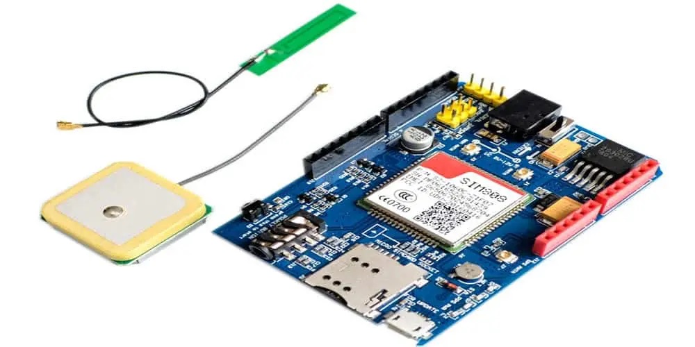
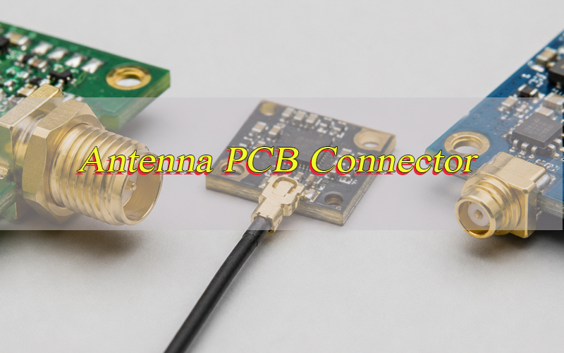
An antenna PCB connector is a board-mounted RF interface that links a wireless circuit to an antenna, coaxial cable or RF test point. It carries high-frequency signals between the radio module, matching network and antenna system.
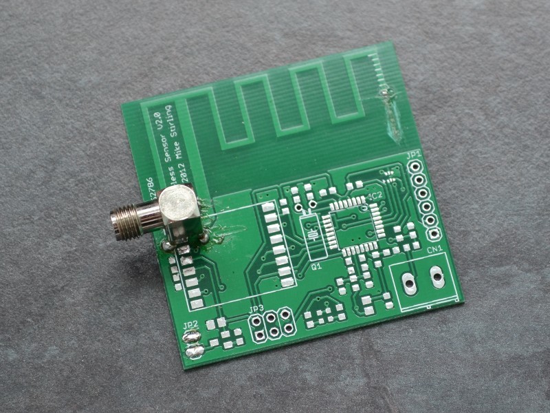
The core function is to maintain a controlled RF path, usually 50Ω, while giving the product a reliable mechanical connection. It may be a U.FL/I-PEX socket, SMA connector, MMCX connector, RF switch connector or board-edge coaxial launch.
In PCBA projects, this part is common in WiFi modules, GSM trackers, IoT gateways, GPS devices, smart meters, medical wireless devices and industrial controllers.
What Types of Antenna PCB Connectors Are Commonly Used?
Common antenna PCB connector types include SMA, RP-SMA, U.FL/I-PEX/MHF, MMCX, MCX, board-edge launch connectors and RF switch connectors. Each option fits a different balance of size, strength, frequency, cost and antenna structure.
For compact wireless PCBA, U.FL or MHF is common. For external antennas and repeated field mating, SMA or RP-SMA is usually safer. MMCX and MCX offer stronger snap-on retention than micro coax connectors while staying smaller than SMA.
| Type | Mount | Strength | Common Use |
|---|---|---|---|
| SMA | Through-hole / edge / panel | High | Routers, gateways, test ports |
| RP-SMA | Through-hole / panel | High | WiFi antennas, consumer wireless |
| U.FL / I-PEX | SMT | Low to medium | IoT, GPS, WiFi modules |
| MHF4 / MHF5 | SMT | Low | Compact 5G, M.2, wearable devices |
| MMCX | SMT / through-hole | Medium | Drones, GPS, RF modules |
| MCX | SMT / through-hole | Medium | RF equipment, test interfaces |
| RF switch | SMT | Low | Production test, diagnostics |
What Are the Advantages and Limits of Antenna PCB Connector?
A connector gives the product flexibility, but it also adds a new RF and mechanical risk point. The benefit is strongest when the product uses external antennas, replaceable antenna cables or production RF test fixtures.
The advantage is design flexibility; the limit is added loss, cost and handling risk. A direct PCB antenna feed may be cheaper, while a connector-based design is easier to tune, test, service and adapt to different markets.
Advantages include:
- External antenna options for weak-signal environments.
- Easier WiFi, GSM, GPS or Bluetooth testing.
- Flexible antenna cable routing inside the enclosure.
- Faster product variants using one PCB platform.
Limits include:
- Extra insertion loss in the RF path.
- Higher BOM and assembly cost.
- Limited mating life for micro connectors.
- Risk of cable damage during PCBA testing.
SMA vs U.FL vs MMCX: Which PCB Antenna Connector Should You Choose?
Choose SMA for strength, U.FL for compact internal cables and MMCX when the product requires a small connector with better retention than U.FL. The right PCB antenna connector depends on enclosure access, mating cycles, vibration, board space and antenna position.
Use SMA for external access, U.FL for internal space saving and MMCX for compact products that still require stronger snap-on retention. This simple rule helps reduce selection errors during early design.
| Option | Size | Mating Style | Advantage | Limit |
|---|---|---|---|---|
| SMA | Large | Threaded | Strong field connection | More board and panel space |
| U.FL | Very small | Snap-on | Saves PCB space | Limited mating cycles |
| MMCX | Small | Snap-on | Better retention than U.FL | Higher cost and larger footprint |
For terms such as SMA-F male antenna PCB connector or SMA-female antenna PCB connector, confirm the exact drawing. SMA gender may describe the body, center contact or reverse-polarity version.
How Should You Select a WiFi Antenna Connector for PCB Assembly?
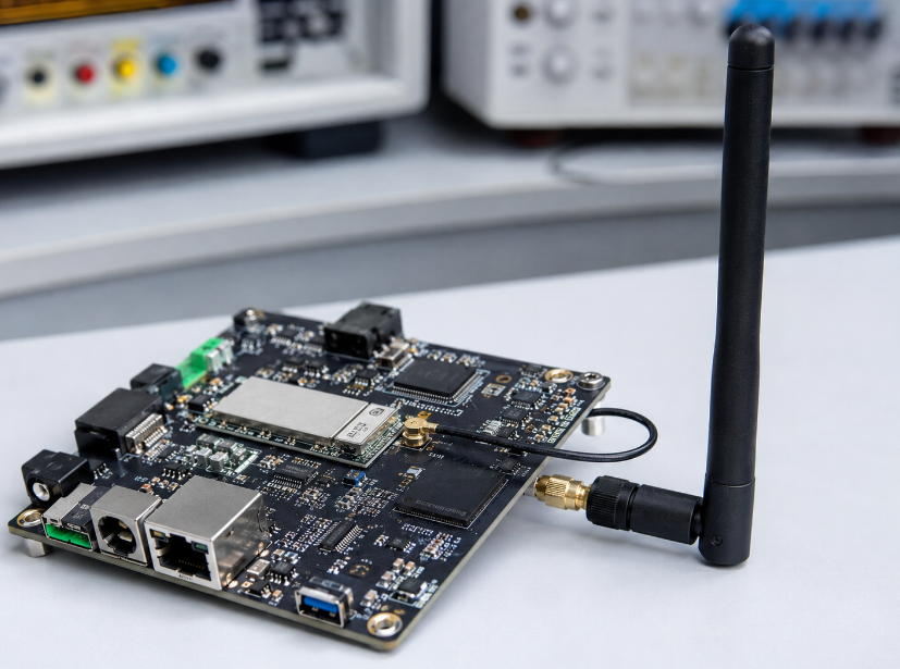
A WiFi antenna PCB connector should match the WiFi band, antenna cable, enclosure, wireless module and final test method. Modern WiFi devices may use 2.4 GHz, 5 GHz or 6 GHz, so the connector and coaxial cable must support the highest working band.
For routers and gateways, SMA or RP-SMA is practical for external antennas. For compact IoT devices, U.FL, I-PEX, MHF4 or MHF5 is usually preferred. In MIMO products, each RF path should follow the same impedance target and cable discipline.
Selection points:
- Use 50Ω RF connectors and coaxial cable.
- Keep the antenna cable short when space allows.
- Confirm mating height and cable plug series.
- Reserve space for cable bending and operator access.
- Test with the final enclosure installed.
How Should GSM Antenna Connectors Be Chosen for Wireless PCB Projects?
A GSM antenna PCB connector should support cellular bands, antenna power level, coaxial cable routing and the mechanical environment. GSM, LTE, NB-IoT and Cat-M products often work across low and high cellular bands, so connector loss and antenna matching must be reviewed together.
For trackers, smart meters and industrial cellular devices, connector retention and cable strain relief matter as much as RF performance. U.FL is common inside compact devices, while SMA is better for external antennas mounted outside the housing.
Practical checks include:
- Confirm all target bands before approving the connector.
- Keep the feed path away from batteries, shields and metal frames.
- Use cable support when the product may vibrate.
- Review antenna gain, cable loss and connector loss together.
- Run conducted and over-the-air tests before mass production.
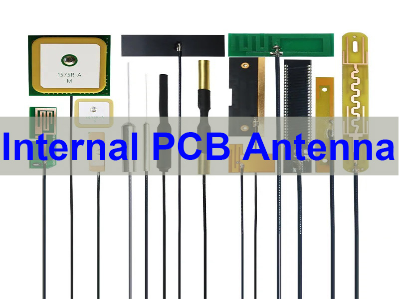
What Type of Connectors Do You Need for PCB Antenna Designs?
The right connector depends on antenna type, board space, enclosure structure, frequency band and test method. Some PCB antenna designs use a direct RF feed, while others need a removable coaxial interface.
PCB antenna designs do not always require the same connector type, and the final choice should match the antenna structure and production test plan.
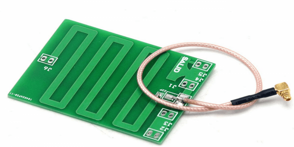
- PCB trace antenna: Usually uses a direct feed from the matching network. An RF test connector may be added for tuning and validation.
- Chip antenna: Often uses a direct feed with a strict keep-out area. The connector is mainly used for testing or alternative antenna versions.
- Flexible antenna: Commonly uses U.FL, I-PEX, MHF4 or MHF5 because these connectors save PCB space and support internal cable routing.
- External antenna: Usually uses SMA, RP-SMA, MMCX or MCX. These connectors are better for products that require stronger mating, external access or field replacement.
- PCB antenna array connector: Used when multiple antenna paths require controlled coaxial feeds, consistent cable length and stable RF matching.
- Compact IoT design: Micro coax connectors are suitable, but mating life, cable bending and assembly access must be checked early.
- Industrial wireless design: SMA or MMCX is safer when the product faces vibration, repeated service or outdoor installation.
The final choice should balance 50Ω matching, antenna position, cable strain, enclosure space and production test reliability.
How to Add Antenna Connectors to a PCB During PCBA Assembly?
Adding antenna connectors to a PCB should be controlled from design review to final wireless testing. Most assembly problems come from wrong footprints, poor soldering, cable stress or uncontrolled mating force. A stable assembly process should confirm the connector footprint, RF layout, solder quality, cable mating method and final wireless test result.
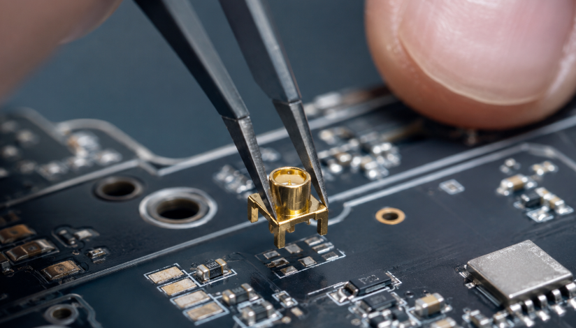
Step 1: Review the connector datasheet, footprint, mated height, cable plug, impedance target and antenna type before PCB fabrication. Confirm that the land pattern matches the selected connector series.
Step 2: Check the RF layout before SMT production. The feed line, ground vias, keep-out area, matching network and cable exit direction should be reviewed together.
Step 3: Print solder paste with controlled volume. Micro RF connectors need accurate paste coverage because excessive solder can cause tilt, while insufficient solder can weaken retention.
Step 4: Place the connector by SMT machine with correct orientation and alignment. Manual correction should be avoided unless inspection rules are clear.
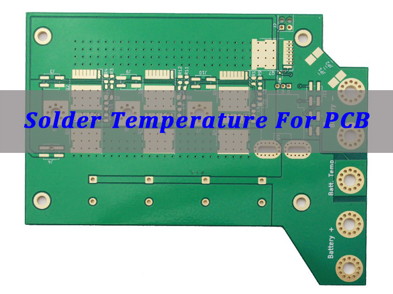
Step 5: Reflow the PCB with a verified temperature profile. The connector body, plastic insulator and solder pads must tolerate the process window.
Step 6: Inspect the connector after reflow. Use AOI, microscope inspection or manual visual inspection to check solder joints, shell position, pad wetting and connector flatness.
Step 7: Mate the antenna cable with controlled vertical force. Avoid angled pressing, twisting or pulling the cable near the connector.
Step 8: Add cable retention when required. Adhesive, foam, clips or enclosure support can reduce cable movement during vibration or final assembly.
Step 9: Run RF and wireless function tests before shipment. The connector should be checked as part of the full antenna system, not as an isolated component.
What Layout Rules Matter for Antenna Connector PCB Design?
Antenna connector PCB design should protect the RF signal path from the wireless IC to the antenna. A correct footprint is not enough if the feed trace, ground return or antenna keep-out area is poorly designed.
Good layout reduces signal reflection, wireless range loss, connector stress and late-stage antenna tuning problems.
- Keep the RF feed controlled at 50Ω. Use the correct trace width, dielectric thickness and ground reference based on the PCB stackup.
- Place the matching network close to the antenna feed. This improves tuning control and reduces extra parasitic effects.
- Keep the RF trace short and direct. Avoid unnecessary bends, stubs, vias and layer transitions.
- Use solid ground reference under the RF path. Broken ground can increase impedance variation and signal loss.
- Add ground vias near the connector. Dense via stitching helps create a stable return path around the connector launch area.
- Reserve antenna keep-out space. Copper, metal shields, batteries and large components near the antenna can detune wireless performance.
- Avoid routing noisy signals near the RF path. Switching power traces, clocks and high-current lines can introduce interference.
- Control cable exit direction. The antenna cable should leave the connector without sharp bending or pressure from the enclosure.
- Check mechanical clearance. The connector must have enough space for mating tools, cable bending and final assembly.
- Validate with the final enclosure. Plastic walls, metal coating, screws and batteries can change RF performance after assembly.
How Does Connector Placement Affect Wireless Signal Performance?
Connector placement affects wireless performance because the RF feed, antenna cable and enclosure create one working system. A connector placed near metal, batteries, displays, motors or switching power circuits can increase loss or detune the antenna.
Place the antenna feed area near a PCB edge or corner when the antenna requires open space. Keep the cable path free from sharp bends, cover pressure and moving parts.
For MIMO WiFi, LTE diversity or antenna array products, separate antenna paths to reduce coupling. In compact devices, verify the final position with the real plastic housing, battery, shielding can and cable path installed.
What PCBA Assembly Challenges Happen With RF Antenna Connectors?
The main PCBA challenges are connector tilt, insufficient solder, lifted pads, cable damage and wrong mating parts. Micro connectors are especially sensitive because the center contact and shell can deform under angled force.
In batch PCBA production, many RF failures come from mating force, cable routing and footprint mismatch, not from the connector body alone. These problems increase rework cost and delay shipment.
Control points include:
- Use the supplier’s recommended land pattern.
- Control solder paste volume on small SMT pads.
- Avoid hand pressure on the center contact.
- Use a mating tool for micro RF connectors when possible.
- Add cable fixtures, adhesive or foam support for vibration products.
- Define rework limits before mass production.
How Should Antenna PCB Connectors Be Tested After Assembly?
Antenna PCB connectors should be tested through visual inspection, mechanical checking, electrical inspection and RF verification. The test method should match the wireless standard, shipment volume and field reliability risk. A reliable test flow should confirm solder quality, mating stability, RF continuity and final wireless performance before mass shipment.
Step 1: Inspect the connector visually after reflow. Check solder wetting, shell flatness, pad alignment, solder bridges, lifted pads and visible body damage.
Step 2: Check the connector position under microscope when using U.FL, I-PEX, MHF or other micro RF connectors. Small tilting can cause poor mating or unstable contact.
Step 3: Test for open and short circuits. The signal pin and ground should not be shorted, and the RF feed should connect correctly to the matching network.
Step 4: Verify cable mating quality. The antenna cable should sit fully on the connector without angled mating, loose retention or shell deformation.
Step 5: Check cable routing and strain. The cable should not be sharply bent, pinched by the enclosure or pulled during product assembly.
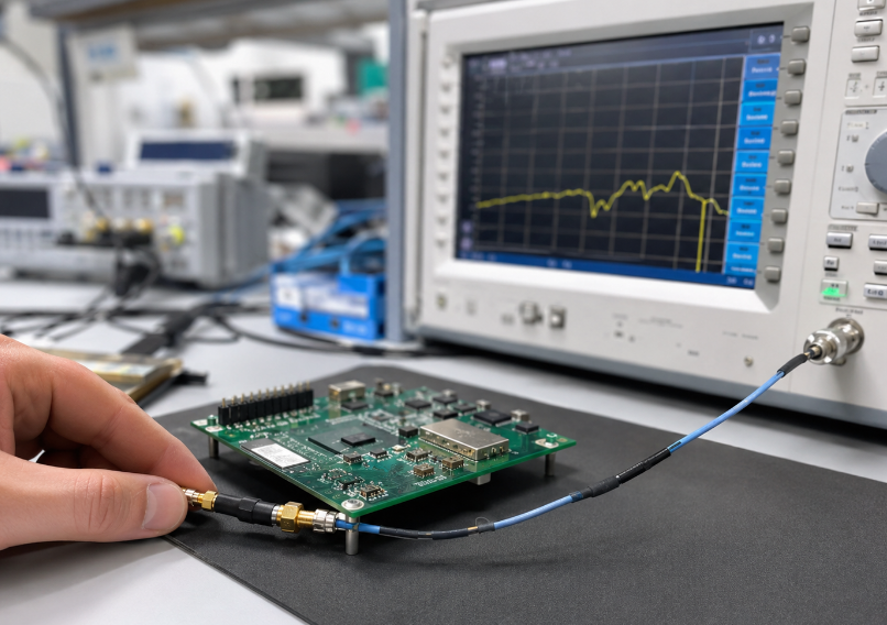
Step 6: Run conducted RF testing when the product design allows it. Return loss, insertion loss or VSWR sampling can help find hidden connector or matching problems.
Step 7: Perform wireless function testing. WiFi, GSM, GPS, Bluetooth, LoRa or NB-IoT tests should confirm that the assembled board communicates normally.
Step 8: Test with the final enclosure installed. The housing, battery, display, metal parts and antenna cable position can all affect real wireless performance.
Step 9: Record failures by type. Separate soldering defects, cable defects, connector damage, antenna tuning problems and enclosure interference to guide process improvement.
What Cost Factors Affect Antenna PCB Connector Projects?
Cost is affected by connector brand, size, plating, frequency rating, cable assembly, antenna type, assembly yield and RF testing level. A cheaper connector may increase total cost if it causes poor mating, unstable RF results or high rework.
The best cost decision compares connector price, cable price, assembly yield, testing time and field reliability together. For volume orders, approved alternatives can reduce supply risk, but they must be validated before substitution.
Main cost factors include:
- Original brand vs qualified equivalent.
- SMA, U.FL, MMCX or custom cable assembly.
- Gold plating and contact durability.
- SMT placement accuracy and inspection level.
- Conducted RF testing or over-the-air testing.
- MOQ, lead time and lifecycle stability.
How to Choose an Antenna PCB Connector Supplier for Wireless PCBA Projects?
Choose a supplier that can support connector selection, PCB manufacturing, PCBA assembly, antenna cable matching and wireless testing. For RF projects, the lowest connector price is not always the lowest project cost.
The best supplier should help prevent connector mismatch, RF instability, assembly rework and procurement delays before they become production problems.
- Check connector sourcing capability. The supplier should provide original brands, qualified alternatives and clear lifecycle control for SMA, U.FL, I-PEX, MHF, MMCX and MCX options.
- Confirm footprint and mating review. The supplier should verify the connector land pattern, mated height, cable plug and drawing before production.
- Evaluate controlled impedance capability. Wireless PCB projects often require 50Ω RF traces, stable stackup and clear impedance reports.
- Review SMT process experience. Micro RF connectors require accurate placement, solder paste control and careful reflow inspection.
- Check antenna cable support. A good supplier can match connector, cable length, cable diameter, antenna type and enclosure routing.
- Ask about RF testing. Conducted testing, wireless function testing and over-the-air checks can reduce shipment risk.
- Review quality traceability. BOM records, incoming inspection, soldering inspection, test reports and failure analysis help control batch consistency.
- Confirm export and compliance support. RoHS materials, IPC-based assembly control and customer-specific inspection rules are important for global projects.
- Check engineering communication speed. RF issues often involve PCB layout, antenna tuning, enclosure design and cable routing, so fast technical feedback matters.
- Choose a real manufacturing partner. A China source factory with PCB, PCBA and sourcing capability can reduce coordination cost and support custom wireless products from prototype to mass production.
FAQs About Antenna PCB Connector Selection and Assembly
Q1: What is the safest antenna connector for a new wireless PCB project?
A1. If the antenna is external, SMA or RP-SMA is safer because it is stronger. If the antenna cable stays inside a compact device, U.FL, I-PEX or MHF is more suitable. Always confirm 50Ω impedance, frequency band, cable plug and enclosure space before layout.
Q2: Can one connector support WiFi, Bluetooth and Zigbee?
A2: Yes, when the product shares one 2.4 GHz antenna path. The connector, cable and antenna must match the same RF design. For MIMO WiFi or separate wireless modules, separate antenna paths may be required.
Q3: Why does the wireless signal become weak after PCBA assembly?
A3: Common causes include poor solder joints, connector tilt, wrong cable, damaged micro connector or cable pressure from the enclosure. Testing should check solder quality, cable mating, RF continuity and final wireless function.
Q4: Is U.FL better than SMA for small products?
A4: U.FL is better for compact internal antenna cables because it saves PCB space. SMA is better for external antennas, repeated mating and field service. The choice depends on space, strength and how the antenna is used.
Q5: Can I replace one RF connector with another brand?
A5: Yes, but only after checking the datasheet. Similar connectors may have different footprints, mated heights and cable plugs. For mass production, approve one main part and one tested alternative before substitution.
Q6: Why does the antenna fail after the enclosure is closed?
A6: Plastic, metal parts, batteries, screws and cable position can change antenna performance. The connector may also be too close to metal. Wireless testing should be done with the final enclosure and antenna cable position.
Q7: Does antenna cable length matter?
A7: Yes. A longer cable can increase RF loss, while a short cable may create sharp bending or connector stress. The best length should balance signal loss, cable routing, bending radius and assembly access.
Q8: What causes a micro antenna connector to pop off?
A8: Angled mating, wrong cable plug, repeated testing, sharp cable bending and missing strain relief are common causes. Use trained operators, vertical mating and cable support to reduce connector and cable damage.
Q9: Should antenna connectors be hand soldered in prototypes?
A9. Hand soldering can work for simple prototypes, but SMT reflow is better for RF validation. It gives more stable results for solder strength, connector flatness and RF testing.
Q10. How do I know if the problem is the connector or antenna design?
A10. Connector problems often show as loose mating, poor soldering, open circuits or damaged cable. Antenna design problems usually show as poor matching or weak signal. Use visual inspection, continuity testing and RF testing together.
Q11. Can one PCB support both internal and external antennas?
A11. Yes. A PCB can use an RF switch, solder jumper or matching option to support different antenna versions. Each version should be tested separately to avoid unused RF stubs and tuning errors.
Q12. What files are needed for an antenna connector PCBA quotation?
A12. Send Gerber files, BOM, connector part number, antenna type, cable drawing, frequency bands, enclosure drawing and test requirements. Clear files reduce wrong connector selection and RF test failure.
Q13. Are low-cost antenna connectors safe for mass production?
A13. They can be used only after testing. Poor plating, weak retention or unstable mating may increase rework cost. A qualified option should pass sample testing, cable mating checks and production trial approval.
Q14. Do outdoor wireless products need special connector protection?
A14. Yes. Outdoor products may need enclosure sealing, panel SMA hardware, gaskets, cable glands or sealed antenna assemblies. Waterproof reliability should be checked at the complete product level.
Antenna PCB connector selection should be reviewed together with RF design, PCB layout, PCBA assembly and final wireless testing. A good choice balances 50Ω matching, frequency range, PCB space, mechanical strength, cable routing and enclosure structure. This helps reduce weak signal, connector damage and assembly rework.
EBest Circuit supports wireless PCB and PCBA projects from connector selection to controlled impedance PCB manufacturing, antenna cable matching, SMT assembly and functional testing. Send your RF PCB, BOM, antenna files or PCBA requirements to sales@bestpcbs.com for a quotation.