

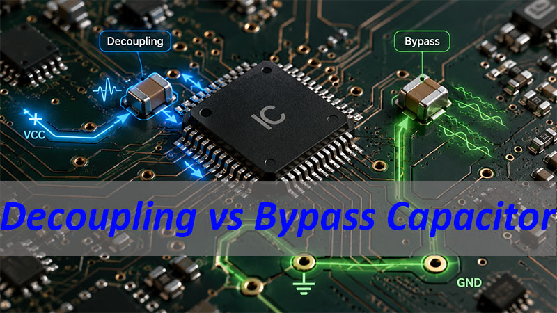
Decoupling vs bypass capacitor is a common question in PCB design because the two terms are often used together. In many circuits, they may even refer to the same physical capacitor placed near an IC power pin.
The simple answer is this: a decoupling capacitor helps reduce the effect of power supply disturbances between circuit blocks, while a bypass capacitor gives high-frequency noise a low-impedance path to ground.
In practical PCB design, one capacitor can often perform both functions. For example, a 100 nF ceramic capacitor placed close to an IC power pin can help stabilize the local power supply and bypass high-frequency noise to ground.
The key difference is not only the capacitor itself. It is more about why the capacitor is used, where it is placed, and what type of noise or power disturbance it needs to control.
What Is a Decoupling Capacitor?
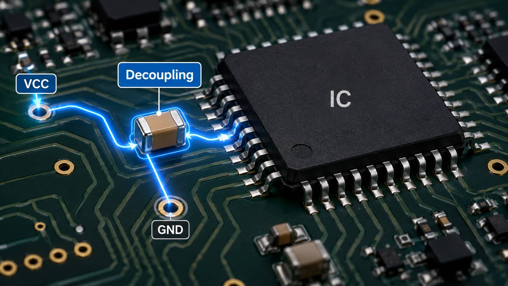
A decoupling capacitor is used to reduce the interaction between different parts of a circuit through the power supply. It helps one circuit block avoid being affected by voltage noise or current changes from another circuit block.
When an IC switches, it may draw current very quickly. This sudden current demand can cause voltage dips or noise on the power rail. A decoupling capacitor provides local charge near the IC, so the power supply voltage stays more stable.
In PCB design, a decoupling capacitor is usually placed between the power pin and ground pin of an IC.
Its main purposes are:
- Stabilize the power supply near the IC
- Reduce voltage dips during switching
- Provide local energy storage
- Reduce noise coupling between circuit blocks
- Improve digital and mixed-signal circuit reliability
For example, microcontrollers, FPGAs, memory chips, high-speed logic ICs, and mixed-signal devices usually need decoupling capacitors close to their power pins. Without proper decoupling, the circuit may have unstable operation, signal noise, reset problems, or EMI issues.
What Is a Bypass Capacitor?
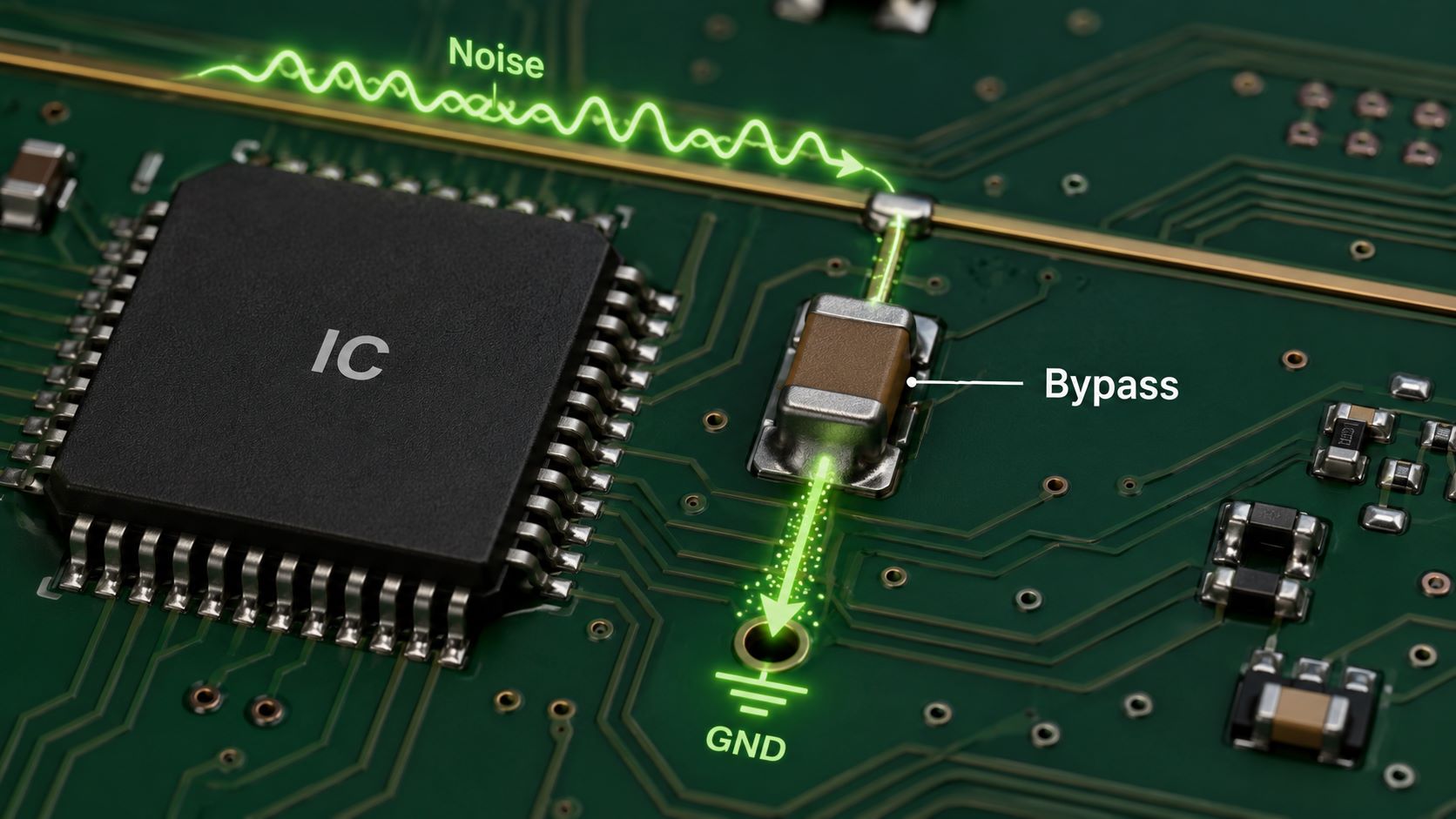
A bypass capacitor is used to send unwanted AC noise to ground. It provides a low-impedance path for high-frequency noise, so the noise does not continue through the power rail or enter sensitive parts of the circuit.
In many PCB circuits, a bypass capacitor is also placed between VCC and ground. For DC voltage, the capacitor blocks current after it is charged. For high-frequency noise, the capacitor behaves like a low-impedance path and allows the noise to return to ground.
Its main purposes are:
- Bypass high-frequency noise to ground
- Reduce ripple on the power rail
- Keep unwanted AC noise away from sensitive circuits
- Improve power integrity
- Reduce high-frequency interference
A bypass capacitor is commonly used near ICs, analog circuits, amplifiers, sensors, power supply inputs, and other noise-sensitive areas.
The word “bypass” emphasizes the noise path. The capacitor allows unwanted high-frequency noise to bypass the active circuit and return to ground.
Decoupling vs Bypass Capacitor: Are They the Same?
Decoupling capacitors and bypass capacitors are closely related, but they are not always exactly the same.
In many PCB designs, the same capacitor can be called both a decoupling capacitor and a bypass capacitor. For example, a 100 nF ceramic capacitor near an IC power pin can decouple the IC from power rail disturbance and also bypass high-frequency noise to ground.
However, the two terms focus on different functions:
| Term | Main Focus | Typical Meaning |
|---|---|---|
| Decoupling capacitor | Isolation between circuit blocks | Reduces power rail disturbance and local voltage fluctuation |
| Bypass capacitor | Noise path to ground | Provides a low-impedance path for high-frequency noise |
| In PCB practice | Often the same component | A capacitor near an IC power pin may perform both functions |
A simple way to understand the difference is:
- Decoupling focuses on keeping the local power supply stable.
- Bypassing focuses on sending unwanted high-frequency noise to ground.
This is why engineers often use the two terms together. The physical capacitor may be the same, but the explanation depends on which problem it is solving.
What Is the Main Difference Between Decoupling and Bypass Capacitors?
The main difference between a decoupling capacitor and a bypass capacitor is the design purpose.
A decoupling capacitor is mainly used to maintain a stable local supply voltage. It provides short bursts of charge when the IC suddenly needs current. This helps reduce voltage drops and prevents one circuit block from disturbing another through the power rail.
A bypass capacitor is mainly used to reduce high-frequency noise. It gives AC noise a short path to ground, so the noise does not travel through the circuit.
The difference can be explained like this:
- Decoupling capacitor: “Keep the IC power supply stable.”
- Bypass capacitor: “Send unwanted high-frequency noise to ground.”
In real PCB design, these two functions often happen at the same time. A capacitor close to the IC power pin can supply local current and reduce high-frequency noise. That is why the two terms are often mixed.
For design work, the more important questions are:
- Is the capacitor close enough to the IC power pin?
- Is the ground connection short and low impedance?
- Is the capacitor value suitable for the noise frequency?
- Is the package suitable for high-frequency performance?
- Is the power and ground plane structure designed properly?
In many cases, good PCB layout matters more than the name used for the capacitor.
How Do Decoupling and Bypass Capacitors Work in a Circuit?
Decoupling and bypass capacitors work because a capacitor behaves differently with DC voltage and AC noise.
For DC power, the capacitor charges and acts like a small local energy reservoir. When the IC suddenly switches and needs current, the capacitor can provide charge quickly. This helps reduce voltage droop at the IC power pin.
For high-frequency noise, the capacitor provides a low-impedance path to ground. This helps keep noise away from the power rail and sensitive signal paths.
A simple process looks like this:
- The IC switches and creates a fast current demand.
- The local capacitor supplies part of this current.
- The voltage change on the power rail is reduced.
- High-frequency noise flows through the capacitor to ground.
- The circuit becomes more stable and less noisy.
The capacitor does not work alone. Its actual performance also depends on:
- Capacitance value
- Capacitor package
- Equivalent series resistance, or ESR
- Equivalent series inductance, or ESL
- Distance from the IC power pin
- Via placement
- Power and ground plane design
- PCB stack-up
For high-frequency circuits, physical layout is very important. Even if the capacitor value is correct, the capacitor may not work well if it is placed too far away from the IC.
Where Should Decoupling and Bypass Capacitors Be Placed on a PCB?
Decoupling and bypass capacitors should be placed as close as practical to the IC power pin and ground return path. The goal is to keep the current loop short and low impedance.
Good placement rules include:
- Place the capacitor close to the IC power pin.
- Connect the capacitor to ground with a short path.
- Keep traces short and wide where possible.
- Avoid long, thin traces between the capacitor and IC.
- Use nearby vias to connect to power and ground planes.
- Place high-frequency, small-value capacitors closest to the IC.
- Place larger-value bulk capacitors near the power rail, regulator output, or power input.
For a typical IC, a common practice is to place a small-value ceramic capacitor, such as 100 nF, near each power pin or power pin group. Here, “small-value” refers mainly to capacitance value, not only physical size.
Larger-value capacitors, such as 1 µF, 4.7 µF, 10 µF, or higher, may be placed near the power rail, regulator output, power input, or a group of ICs. These capacitors help support lower-frequency voltage changes and provide more local energy storage.
Poor placement can reduce capacitor effectiveness. A decoupling capacitor placed far from the IC may still appear in the schematic, but it may not help much at high frequency because the trace inductance is too high.
For PCB layout, the practical rule is simple: the capacitor should be close to the noise source and close to the ground return path.
What Capacitor Values Are Commonly Used?
Common capacitor values depend on the circuit speed, power rail, IC type, noise frequency, and PCB layout. There is no single value that works for every design.
However, some values are widely used in PCB design:
| Common Value | Also Written As | Typical Use |
|---|---|---|
| 10 nF | 0.01 µF | Higher-frequency bypassing |
| 100 nF | 0.1 µF | Common IC decoupling capacitor |
| 1 µF | 1,000 nF | Local power rail support |
| 4.7 µF | 4,700 nF | Bulk decoupling near IC groups |
| 10 µF | 10,000 nF | Power input or rail stabilization |
| 47 µF or higher | 47,000 nF or higher | Bulk energy storage and low-frequency filtering |
A common design approach is:
- Use a 100 nF ceramic capacitor near the IC power pin for local high-frequency decoupling.
- Add 1 µF to 10 µF capacitors near power rails, regulator outputs, or IC groups for local energy support.
- Use 47 µF or larger bulk capacitors near power inputs or regulator outputs for lower-frequency filtering and energy storage.
In this context, “small capacitor” and “large capacitor” usually refer to capacitance value. A 100 nF capacitor is a small-value capacitor. A 10 µF or 47 µF capacitor is a larger-value capacitor.
Capacitance and physical size are related, but they are not exactly the same. In the same capacitor type, voltage rating, dielectric material, and product series, a larger capacitance value often requires a larger package. However, physical size also depends on capacitor type, voltage rating, dielectric, temperature performance, DC bias behavior, and manufacturer design.
For example, a 10 µF ceramic capacitor may be available in a small SMD package, but its effective capacitance can drop under DC bias. A larger package or different capacitor type may be needed if stable capacitance is important.
How to Choose the Right Decoupling or Bypass Capacitor?
Choosing a decoupling or bypass capacitor requires more than selecting a common value. The right choice depends on the circuit, frequency, power rail, capacitor type, and PCB layout.
Check these points first:
- Circuit function
Digital ICs, analog circuits, RF circuit boards, and power circuits may need different capacitor values and placement methods. - Capacitance value
100 nF is common for local IC decoupling, but larger or smaller values may be needed depending on the frequency range. - Capacitor type
MLCC ceramic capacitors are widely used for high-frequency decoupling. Tantalum, aluminum electrolytic, and polymer capacitors may be used for larger capacitance or bulk support. - Dielectric type
X7R and X5R MLCCs are common for decoupling. C0G/NP0 capacitors are more stable, but they usually have smaller capacitance values. - Voltage rating
Choose a voltage rating higher than the working voltage. Avoid using capacitors too close to their rated voltage limit. - DC bias behavior
MLCC capacitance can drop when DC voltage is applied. This is important for power rail decoupling. - Package size
Smaller packages often have lower ESL and better high-frequency performance, but they may have lower effective capacitance. - Placement
A well-placed capacitor often performs better than a theoretically correct capacitor placed far away. - Ground connection
Use a short, direct ground return path. Poor grounding can reduce bypass performance.
For many digital PCB designs, a practical starting point is to place a 100 nF ceramic capacitor close to each IC power pin or power pin group. This small-value capacitor helps reduce high-frequency noise near the IC.
Larger-value capacitors, such as 1 µF, 4.7 µF, or 10 µF, may be added near the power rail, regulator output, or IC groups to support lower-frequency voltage changes and provide more local energy storage.
For critical high-speed, RF, automotive, medical, or industrial products, capacitor selection should be checked against the IC datasheet, power integrity requirements, PCB stack-up, and layout review.
Common PCB Layout Mistakes with Decoupling and Bypass Capacitors
Many decoupling problems are not caused by the capacitor value. They are caused by PCB layout.
Common mistakes include:
- Placing the capacitor too far from the IC
Long traces add inductance and reduce high-frequency performance. - Using a long ground return path
A poor ground path increases loop area and noise. - Using long, thin traces unnecessarily
Long and narrow traces increase impedance. - Putting vias in the wrong location
Via placement affects the current loop. Ground vias should be close and direct. - Using only one bulk capacitor for many ICs
A bulk capacitor alone cannot handle local high-frequency switching noise at each IC. - Ignoring capacitor package parasitics
Larger physical capacitors may not work well at high frequency because of higher ESL. - Confusing capacitance value with physical size
A larger capacitance value does not automatically mean better high-frequency performance. Package size, ESL, ESR, and placement also matter. - Copying the schematic without layout review
A correct schematic does not guarantee good power integrity. - Not checking the IC datasheet
Some ICs require specific decoupling values and placement instructions.
A better layout approach is:
- Place small-value ceramic capacitors closest to the IC power pins.
- Keep the loop between the power pin, capacitor, and ground as short as possible.
- Use a solid ground plane when possible.
- Add larger-value bulk capacitors near regulators or power entry points.
- Review decoupling placement during DFM and layout checking.
For PCB assembly, capacitor polarity, package, footprint, and placement should also be checked before production. A wrong footprint or wrong capacitor orientation can cause assembly defects or circuit failure.
FAQs About Decoupling vs Bypass Capacitor
What Is the Difference Between a Decoupling Capacitor and a Bypass Capacitor?
A decoupling capacitor helps isolate circuit blocks from power supply disturbances. A bypass capacitor provides a low-impedance path for high-frequency noise to ground. In many PCB designs, the same capacitor can perform both functions.
Are Decoupling and Bypass Capacitors the Same?
They are often the same physical capacitor, especially when placed near an IC power pin. The difference is mainly in the function being described. Decoupling focuses on supply stability, while bypassing focuses on noise removal.
Why Is a 100 nF Capacitor Commonly Used?
A 100 nF capacitor, also written as 0.1 µF, is commonly used because it works well for local IC decoupling in many digital circuits. It is small in capacitance value, widely available, and effective for reducing high-frequency noise when placed close to the IC.
Does “Small Capacitor” Mean Small Size or Small Capacitance?
In decoupling discussions, “small capacitor” usually means small capacitance value, such as 10 nF or 100 nF. The physical size may also be small, but size depends on package, voltage rating, dielectric type, and manufacturer design.
Are Larger-Value Capacitors Always Physically Larger?
Not always. In the same capacitor type and voltage rating, larger capacitance often needs a larger package. However, physical size also depends on dielectric material, capacitor structure, voltage rating, temperature performance, and DC bias behavior.
Where Should a Bypass Capacitor Be Placed?
A bypass capacitor should be placed close to the IC power pin and connected to ground through a short, low-impedance path. Poor placement can reduce its high-frequency performance.
Where Should a Decoupling Capacitor Be Placed?
A decoupling capacitor should be placed near the power pin of the IC or circuit block it supports. The goal is to provide local charge and reduce power rail disturbance.
Can I Use One Capacitor for Both Decoupling and Bypassing?
Yes. In many PCB designs, one capacitor can serve both purposes. A ceramic capacitor close to an IC power pin can stabilize the local supply and bypass high-frequency noise to ground.
What Value Should I Use for a Decoupling Capacitor?
A common starting value is 100 nF for local IC decoupling. Larger values such as 1 µF, 4.7 µF, or 10 µF may be added for lower-frequency support or bulk decoupling.
Is a Larger Capacitance Value Always Better?
No. Larger capacitance does not always mean better high-frequency performance. Package size, ESL, ESR, placement, and frequency behavior also matter.
Do All ICs Need Decoupling Capacitors?
Most digital ICs and many analog ICs need decoupling capacitors. The exact value and placement should follow the IC datasheet and PCB layout requirements.
What Happens If I Do Not Use Decoupling Capacitors?
The circuit may suffer from voltage dips, noise, unstable logic operation, EMI problems, false triggering, reset issues, or poor signal integrity.
In a nutshell, decoupling vs bypass capacitor is mainly a difference in function. A decoupling capacitor helps stabilize the local power supply, while a bypass capacitor provides a low-impedance path for high-frequency noise to ground.
In practical PCB design, the same SMD ceramic capacitor often performs both jobs, especially when placed close to an IC power pin. For many digital circuits, a 100 nF ceramic capacitor is a common starting point for local high-frequency decoupling, while larger-value capacitors may be added near power rails or regulator outputs for extra energy support.
The key is not only choosing the right capacitance value. Placement, package size, ground path, power plane design, and circuit frequency all affect capacitor performance. For high-speed, RF, industrial, medical, or automotive electronics, capacitor selection and PCB layout should be reviewed carefully before production.
Need medical PCB assembly services, BOM review, capacitor selection, or DFM checking? Pls feel free to send your Gerber files, BOM, stack-up, and project requirements to EBest Circuit (Best Technology) at sales@bestpcbs.com.
You may also like

Tags: bypass capacitor, decoupling capacitor, Decoupling vs Bypass Capacitor