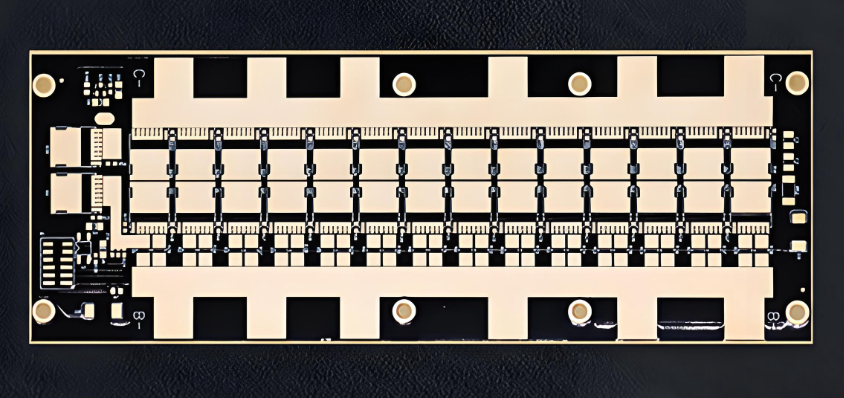
Looking for an ISO 9001 SinkPAD PCB manufacturer in China? EBest Circuit manufactures custom copper-core SinkPAD PCBs with direct thermal paths for high-power LEDs and power electronics.
With free DFM checks, controlled manufacturing, quality testing, and PCB assembly services, we help you address copper pedestal accuracy, thermal contact, and production consistency before they become costly problems.
What SinkPAD PCB Manufacturing Services Does EBest Circuit Offer?
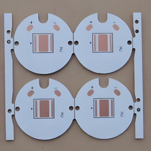
EBest Circuit provides custom SinkPAD PCB fabrication, prototyping, and assembly services, from engineering samples to mass production. Whether you need bare PCBs or fully assembled boards, our services cover the essential stages of your project.
- PCB Engineering Review & Free DFM Review: Check copper pedestal dimensions, thermal pad compatibility, electrical insulation, and stackup before fabrication.
- Custom SinkPAD PCB Fabrication: Manufacture single-layer, double-sided, and multilayer copper-core PCBs with direct thermal paths.
- PCB Prototyping: Produce engineering samples for dimensional, electrical, and thermal evaluation.
- Mass Production: Manufacture production orders using approved drawings, materials, and inspection requirements.
- Component Sourcing: Source LEDs, power semiconductors, connectors, and other electronic components.
- PCB Assembly & Testing: Provide SMT/THT assembly, soldering inspection, and functional testing according to your product requirements.
Gerber files, component specifications, and assembly drawings can be submitted together for a complete PCB manufacturing and assembly quotation.
Why Choose EBest Circuit as Your ISO 9001 SinkPAD PCB Manufacturer in China?
An ISO 9001 SinkPAD PCB manufacturer should offer more than a quality certificate. Your supplier must also understand how copper pedestal accuracy, electrical insulation, and manufacturing consistency affect the finished product.
EBest Circuit brings more than 20 years of PCB manufacturing experience, with engineering support and production services tailored to metal-core PCB projects.
- Stable Manufacturing Quality: Controlled materials, production specifications, and inspection records help maintain consistency between prototype and production orders.
- Free DFM Check: Identify copper pedestal, insulation, and assembly problems before fabrication to reduce unnecessary redesign and production delays.
- Direct Thermal Path Manufacturing: Obtain custom copper-core structures matched to your component’s thermal pad and circuit layout.
- Engineering Support: Get practical recommendations on pedestal geometry, stackup, tolerances, and manufacturing limitations.
- One-Stop PCB & PCBA Services: Reduce supplier coordination by combining PCB fabrication, component sourcing, assembly, and testing.
- Prototype to Mass Production: Verify your design with samples before committing to larger production quantities.
Your board specifications, critical dimensions, and quality requirements can be reviewed before quotation, giving you a clearer manufacturing plan from the start.
Which Quality Certifications Does EBest Circuit Hold for PCB Manufacturing?
EBest Circuit’s quality management certifications include ISO 9001:2015, ISO 13485:2016, IATF 16949, and AS9100D. These certifications support different customer and industry requirements, while SinkPAD PCB quality is assessed against the approved product specifications.
- ISO 9001:2015: Supports quality management, production control, material traceability, inspection, and corrective actions.
- ISO 13485:2016: Covers quality management requirements relevant to medical device manufacturing.
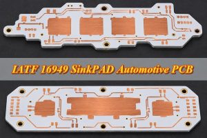
- IATF 16949: Supports automotive quality management requirements within the applicable certification scope.
- AS9100D: Addresses quality management requirements associated with aerospace manufacturing.
- UL: Applicable product recognition can be checked against the relevant listing and product scope.
- RoHS and REACH: Compliance documentation is available for review according to the specified materials and product requirements.
Applicable certificate copies and quality documentation can be requested during supplier qualification. The certified entity, production site, scope, and validity should match your project.
ISO 9001:2026 is the current edition of the standard. Existing ISO 9001:2015 certifications may remain valid during the transition period, subject to their certification status.
What Types of SinkPAD PCB Can EBest Circuit Manufacture?
EBest Circuit manufactures copper-core SinkPAD PCBs in different circuit-layer configurations. The best construction depends on routing density, component placement, and how the board connects to its heat sink.
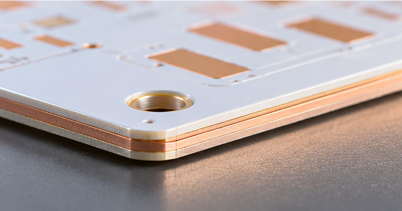
- 1-Layer SinkPAD PCB: One circuit layer on one side of the copper base, suitable for high-power LED and COB modules with straightforward routing.
- 2-Layer Same-Side SinkPAD PCB: Two circuit layers on the same side of the copper base, providing additional routing space.
- 2-Layer Double-Sided SinkPAD PCB: One circuit layer on each side of the copper base, supporting components on both sides.
- 4-Layer Same-Side SinkPAD PCB: Four circuit layers on one side of the copper base for more complex circuit layouts.
- 4-Layer Double-Sided SinkPAD PCB: Two circuit layers on each side of the copper base for designs requiring denser double-sided routing.
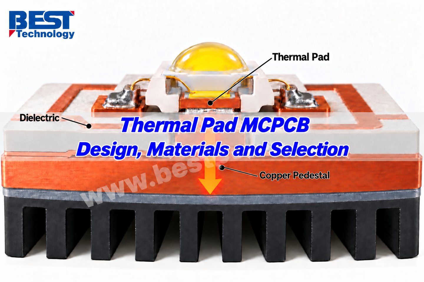
Unlike conventional MCPCBs, SinkPAD PCBs use a copper pedestal to create a direct thermal path from a compatible component thermal pad to the copper base.
For double-sided structures, heat-sink placement and electrical connections between opposite sides require particular attention. Conventional plated through-holes through the copper core are not used in EBest Circuit’s standard double-sided SinkPAD construction.
What Are EBest Circuit’s SinkPAD PCB Manufacturing Capabilities?
EBest Circuit offers custom copper-core SinkPAD PCB manufacturing with different board thicknesses, circuit copper weights, and surface finishes.
| Manufacturing Parameter | 1-/2-Layer SinkPAD PCB | Multilayer SinkPAD PCB |
|---|---|---|
| Copper Base Thickness | 0.8, 1.0, 1.2, 1.4, 1.5 mm | 1.2, 1.4, 1.5, 1.6 mm |
| Finished Board Thickness | 1.0–2.0 mm | 1.6–2.0 mm |
| Circuit Copper Thickness | 0.5, 1, 2 oz; special 3–10 oz subject to confirmation | 0.5, 1, 2, 3 oz |
| Maximum Panel Size | 600 × 500 mm | 600 × 500 mm |
| Surface Finish | Immersion Gold, ENEPIG, Immersion Tin, OSP | Immersion Gold, ENEPIG, Immersion Tin, OSP |
| Profile Processing | Routing, Punching, V-Cut | Routing, Punching, V-Cut |
Copper pedestal height, flatness, position, trace width, spacing, and other critical tolerances are evaluated against your actual drawings. Special constructions and copper weights require engineering confirmation.
What SinkPAD PCB Manufacturing Challenges Can EBest Circuit Solve?
A SinkPAD PCB can meet its electrical specifications yet still develop thermal or assembly problems if the copper pedestal is poorly designed. EBest Circuit addresses these risks through DFM review, precision fabrication, and inspection of critical features.
- Poor Thermal Contact: An uneven or incorrectly sized pedestal can leave gaps beneath the component’s thermal pad, increasing thermal resistance. We check pedestal height, contact dimensions, and machining tolerances to improve the mounting interface.
- Electrical Insulation Failure: Insufficient clearance between the copper pedestal and surrounding circuits can cause short circuits. We review electrical connections, insulation requirements, and circuit spacing before production.
- Copper Pedestal Misalignment: An offset pedestal can interfere with component placement and soldering. Controlled machining, layer alignment, and dimensional inspection help maintain the specified position.
- PCB Warpage: Uneven copper distribution and manufacturing stress can affect board flatness and heat-sink contact. Stackup review and process control help reduce these risks.
- Inconsistent Batch Quality: Material substitutions or dimensional variations can affect repeat orders. Approved specifications, revision control, and inspection records help maintain manufacturing consistency.
These checks are particularly useful when converting a conventional MCPCB design into a direct thermal path PCB or preparing a new SinkPAD construction for volume production.
How Does EBest Circuit Inspect and Test SinkPAD PCB Quality?
EBest Circuit checks critical materials, circuit features, copper pedestal dimensions, and electrical performance during SinkPAD PCB manufacturing. Additional thermal or reliability testing can be arranged when your application requires it.
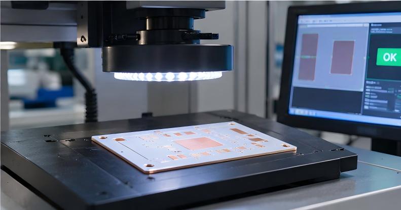
- Incoming Material Inspection: Verify copper-base thickness, insulation materials, and material specifications.
- Copper Pedestal Inspection: Check pedestal height, position, flatness, and contact dimensions against the approved drawing.
- AOI Inspection: Detect circuit pattern defects, including unwanted copper, opens, and shorts.
- Electrical Testing: Verify circuit continuity and required electrical isolation.
- Microsection Inspection: Examine layer structures and critical interfaces when required for the design.
- Thermal Testing: Measure temperature or thermal performance under specified power, mounting, and environmental conditions.
- Final Inspection: Check board dimensions, surface finish, solder mask, and appearance before shipment.
Inspection reports, electrical-test records, and certificates of conformity can be included as agreed order deliverables. Thermal and other specialized tests should be defined before production, including the test method and acceptance criteria.
How Did EBest Circuit Support a Copper-Base LED PCB Project?
Project Background
A U.S. customer was developing a compact high-power LED lighting module and needed a copper-base PCB that could fit the enclosure and maintain effective heat transfer.
The project required prototype verification before moving to a larger production order.
Project Requirements & Challenges
The PCB specifications included:
- Copper Base: 1.5 mm thick.
- Circuit Copper: 2 oz.
- Dielectric Film: 100 μm thick, rated at 3 W/(m·K).
- Surface Finish: OSP.
- Other Requirements: White solder mask, black silkscreen, and individual-board delivery.
The main challenge was maintaining the specified thermal and insulation structure. The customer did not permit pure adhesive substitution, as it would change the approved material construction.
The board also needed to fit the LED module and provide suitable contact with the heat-spreading surface.
EBest Circuit’s Solution
- Material Verification: Confirmed the copper base, dielectric film, circuit copper, and surface finish before fabrication.
- Engineering Review: Submitted production files for customer approval to avoid discrepancies in materials and board construction.
- Prototype Manufacturing: Produced 10 sample boards for LED mounting, enclosure fit, thermal contact, solderability, and electrical evaluation.
- Production Control: Retained the approved material specifications and design revision for the subsequent order.
Project Results
- Prototype Delivery: 10 boards completed within 10 working days.
- Repeat Order: 500 boards completed within 15 working days after sample approval.
- Quality Documentation: Certificate of conformity and electrical-test report supplied with the order.
- Customer Outcome: The project progressed from sample validation to repeat production using the approved materials and board construction.
This project involved a thermoelectric-separation copper-base PCB rather than a confirmed raised-pedestal SinkPAD design. For SinkPAD projects, EBest Circuit also checks copper pedestal geometry, thermal-pad compatibility, and electrical isolation before manufacturing.
How Long Does SinkPAD PCB Manufacturing Take at EBest Circuit?
EBest Circuit provides prototype and mass-production services for different SinkPAD PCB structures. Manufacturing lead time varies with circuit layers, copper pedestal complexity, materials, and order quantity.
| SinkPAD PCB Type | Prototype lead time | Mass-production lead time |
|---|---|---|
| 1-Layer SinkPAD PCB | 1.5–2 weeks | 2–3 weeks |
| 2-Layer Same-Side SinkPAD PCB | 1.5–2 weeks | 2–3 weeks |
| 2-Layer Double-Sided SinkPAD PCB | 1.5–2 weeks | 2–3 weeks |
| Multilayer SinkPAD PCB | 3–4 weeks | 4–6 weeks |
Manufacturing lead time starts after the design and production requirements are approved, subject to material availability and order scheduling.
Component procurement, PCB assembly, international shipping, and customs clearance are not included in the bare-board manufacturing periods.
What Information Is Needed for an Accurate SinkPAD PCB Quotation?
A SinkPAD PCB quotation needs more than Gerber files and board dimensions. The copper pedestal, component thermal pad, and electrical isolation requirements must also be defined to avoid unexpected manufacturing changes.
Please provide:
- PCB Design Files: Gerber or ODB++ files, drill data, board outline, and stackup.
- Copper Pedestal Details: Shape, dimensions, height, location, and critical tolerances.
- Component Information: LED or semiconductor part numbers, thermal-pad specifications, and operating conditions.
- Manufacturing Requirements: Copper-base thickness, circuit copper weight, surface finish, and insulation specifications.
- Quality Requirements: Critical acceptance criteria, inspection reports, and any additional testing.
- Order Details: Prototype or production quantity, required delivery date, and delivery location.
- Assembly Files: BOM, placement files, assembly drawings, and functional-test requirements if PCBA is needed.
EBest Circuit can review your files, identify manufacturing concerns, and prepare a quotation for the agreed board structure and service scope.
FAQs About ISO 9001 SinkPAD PCB Manufacturing
Q1: Can aluminum replace copper in a SinkPAD PCB?
A1: EBest Circuit’s standard SinkPAD constructions use copper. Aluminum does not support the same pedestal-forming process as readily, so an aluminum-based alternative requires a different manufacturing assessment.
Q2: Is lead-free HASL suitable for a 1-layer SinkPAD PCB?
A2: Lead-free HASL is generally not recommended for this construction because of thermal-processing and reliability concerns. OSP or another compatible surface finish is usually preferred.
Q3: Can a SinkPAD PCB use a recessed copper contact instead of a raised pedestal?
A3: Yes, recessed copper features can be considered for suitable designs. The contact geometry and manufacturing method must be reviewed before fabrication.
Q4: Can a 1-layer SinkPAD PCB support chip-and-wire assembly?
A4: Yes. Suitable structures can support chip-and-wire applications, provided the die-attach surface, bond-pad finish, and assembly temperatures meet the component requirements.
Q5: Can the back of a copper-core SinkPAD PCB remain exposed?
A5: Yes. Exposed copper can provide direct contact with a heat sink or mounting surface. Surface protection, corrosion risk, and electrical safety must be considered.
Q6: Do copper-core SinkPAD PCBs require different SMT reflow settings?
A6: They may. Copper’s high thermal mass affects heating and cooling, so the reflow profile should be checked on representative assemblies to protect solder joints and components.
Q7: Can LEDs be replaced on an assembled SinkPAD PCB?
A7: Rework may be possible using controlled preheating and soldering temperatures. Excessive heat or mechanical force can damage the thermal interface and nearby components.
Q8: How should SinkPAD PCBs be stored before assembly?
A8: Store the boards in clean, protective packaging and follow the handling requirements of the selected surface finish. Avoid contamination of solderable pads and copper contact surfaces.
For custom ISO 9001 SinkPAD PCB manufacturer services in China, contact EBest Circuit at sales@bestpcbs.com. We provide copper-core SinkPAD PCB fabrication, free DFM checks, prototyping, mass production, and PCB assembly services. Send your design files, quantity, required delivery date, and delivery location to receive a manufacturing review and quotation.