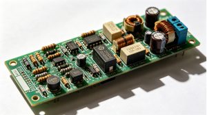
IC package types are the physical formats that protect a semiconductor die and connect it to a printed circuit board. The package determines how many terminals are available, how much board area the component occupies, how heat reaches the PCB, and whether solder joints remain visible after assembly. DIP, SOP, QFP, QFN, LGA, BGA, and CSP packages therefore require different footprints, routing methods, stencil decisions, reflow controls, and inspection plans.
Do not release a footprint from the package name alone. Check the manufacturer’s drawing for terminal dimensions, pitch, coplanarity, thermal-pad requirements, and the recommended land pattern. Match the library part to the full ordering code, then confirm that printing, placement, reflow, cleaning, and inspection can produce and verify the joints.
What Are IC Package Types and Why Do They Matter in PCB Design?
An IC package type defines the component’s body and terminals, which directly control its footprint, routing, thermal path, assembly, and inspection. It is different from the silicon function inside the package. The same circuit may be offered in several packages so a designer can trade board area, thermal performance, electrical parasitics, assembly accessibility, and cost.
Keep three things separate. The physical package is the purchased component. The land pattern or footprint defines its copper pads, solder mask, paste, courtyard, and assembly data. The solder joint is the connection produced on the line. A correct component on the wrong footprint can still fail.
Package choice also changes routing. Perimeter-leaded devices let traces escape outward, while an area-array BGA may require routing channels between pads, via-in-pad, blind microvias, or additional signal layers. A package with an exposed thermal pad may need a controlled copper area and thermal-via pattern. These decisions affect stackup, fabrication cost, assembly process windows, rework access, and inspection coverage.
How Many IC Package Types Are Commonly Used and How Are They Classified?
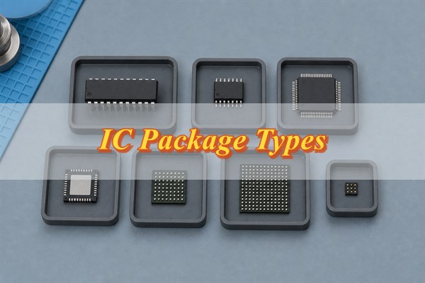
Seven broad families are compared here—DIP, SOP, QFP, QFN, LGA, BGA, and CSP—but no fixed total exists because each family has many variants. A practical classification starts with mounting method and terminal structure instead of trying to count every body size.
- Classify the mounting method. Through-hole packages use leads inserted into drilled holes. Surface-mount packages connect to pads on the board surface. Direct-attach and advanced packages may use bumps, balls, or redistribution structures closer to the die scale.
- Classify the terminal location. Terminals may appear on two sides, four sides, around the underside perimeter, or across an underside grid.
- Classify the terminal form. Common forms include straight pins, gull-wing leads, J-leads, flat lands, solder balls, and bottom contacts.
- Classify the body scale. Conventional molded packages, chip-scale packages, and wafer-level formats create different handling, warpage, and board-design constraints.
- Confirm the exact variant. Body width, lead span, pitch, height, thermal pad, ball map, and pin count can differ within one family.
DIP, SOP or SOIC, QFP, QFN or DFN, LGA, BGA, and CSP cover many routine assembly jobs. Each label is only a family name, not a manufacturing definition. Release decisions still depend on the manufacturer’s exact package code and controlled drawing.
How Do DIP, SOP, QFP, QFN, LGA, BGA, and CSP Packages Compare?
These packages mainly differ in mounting style, terminal geometry, connection density, thermal path, inspectability, and routing demand. The comparison below supports initial selection, but it does not replace the package drawing or assembly capability review.
| Package | Terminal Format | Mounting | PCB / Routing Impact | Assembly and Inspection | Typical Trade-Off |
| DIP | Two rows of pins | Through-hole | Drilled holes and wider body; simple routing | Visible joints; hand, wave, or selective soldering may be used | Easy to inspect and service, but consumes board area |
| SOP / SOIC | Gull-wing leads on two sides | Surface mount | Moderate density with accessible fan-out | Joints are generally visible to AOI | Practical assembly, but lower density than bottom-terminated packages |
| QFP | Gull-wing leads on four sides | Surface mount | Moderate-to-high perimeter pin count; outward fan-out | Lead coplanarity and bridge control matter; joints remain visible | Inspectable, but fine leads can bend and demand precise printing |
| QFN | Bottom lands, often with exposed pad | Surface mount | Compact footprint and short connections; thermal-pad design may dominate | Limited side fillet; X-ray may support hidden-joint evaluation | Good density and, with a designed exposed pad, an effective thermal path; process visibility is lower |
| LGA | Flat underside lands | Surface mount | Dense bottom contacts; escape strategy depends on land map | Hidden joints require process control; X-ray and electrical tests provide complementary evidence | Low profile, but solder volume, coplanarity, and warpage need control |
| BGA | Underside solder-ball grid | Surface mount | High I/O density; may require fine vias, via-in-pad, or more layers | Joints are hidden; X-ray and electrical tests become important | High I/O count per board area, but routing and rework are more demanding |
| CSP | Package-dependent lands or balls within chip-scale size limits | Surface mount | Very small footprint; fan-out depends on whether the CSP uses lands, balls, or a wafer-level layout | Printing, placement, warpage, moisture, and inspection need close control | Chip-scale size, but construction-specific manufacturing limits must be checked |
DIP and SOP are easier to probe, route, and rework. QFP accommodates more connections while keeping the leads visible. QFN and LGA save space and shorten connections, but their critical joints sit beneath the body. BGA and CSP raise connection density further, making footprint control, fabrication, reflow, X-ray inspection, and repair planning more demanding.
How Can You Identify IC Package Types by Body, Leads, Pitch, and Markings?
Identify a package by combining its body geometry, terminal form, terminal count, pitch, dimensions, and manufacturer marking. Visual appearance alone is unreliable because different families can share similar outlines, and one family may contain several pitches or body sizes.
- Read the complete device marking. Record the top code, logo, orientation mark, and any secondary lot or date information without assuming the shortest code is the orderable part number.
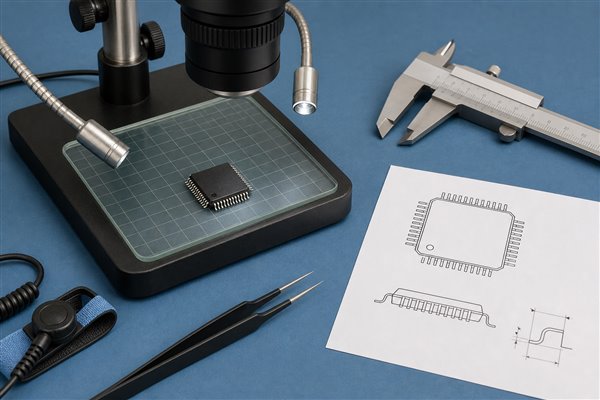
- Inspect the terminal structure. Look for through-hole pins, two-sided gull-wing leads, four-sided leads, bottom lands, or a ball grid. Use magnification when the body hides terminal edges.
- Measure the body and lead span. Check length, width, height, lead-to-lead span, terminal width, and exposed-pad dimensions with suitable calibrated equipment.
- Determine pitch correctly. Measure center-to-center terminal spacing across multiple terminals when possible, then divide by the number of intervals to reduce single-point error.
- Locate the manufacturer package drawing. Match the measured features, pin count, orientation scheme, and dimensional tolerances to the exact orderable code.
- Verify the footprint source. Confirm that the CAD library item was built from the same drawing revision and not from a visually similar package.
If the underside is accessible, a bottom view can separate QFN or LGA lands from a BGA ball grid; X-ray can help when the joints are hidden. Body size alone is poor evidence. A mistaken identification can reverse pin numbering, omit an exposed pad, use the wrong pitch, or produce a plausible-looking footprint that will not solder reliably.
Which IC Chip Package Types Suit Different PCB Assembly Requirements?
The best IC chip package type is the one that meets electrical, thermal, mechanical, inspection, repair, and production-volume requirements together. Selecting only for minimum board area can create a package that the available PCB stackup or assembly line cannot build consistently.
- Prototypes and educational hardware: DIP, larger-pitch SOP, and accessible QFP packages simplify probing, manual rework, and visual inspection.
- General industrial control: SOP, QFP, and appropriately sized QFN packages can balance density, cost, sourcing, and serviceability.
- Compact portable products: QFN, LGA, BGA, and CSP reduce area, but need verified fine-pitch fabrication, printing, placement, reflow, and inspection capability.
- High-I/O processors and FPGAs: BGA often supports the required connection count, although fan-out may force additional layers, smaller vias, or HDI construction.
- Power devices: Packages with exposed pads or dedicated thermal connections can transfer heat into the PCB when copper, vias, interface conditions, and airflow are designed as one thermal path.
- Repair-sensitive equipment: Visible-lead packages may reduce inspection and rework difficulty, even when they use more board area.
Geometry is only half of the selection. Check the full manufacturer part number, lifecycle status, authorized sources, moisture sensitivity, packing method, and any alternate-package plan. A functionally equivalent device in another package is not a drop-in replacement: its footprint, pin map, thermal path, firmware assumptions, and assembly route all need a fresh review.
How Do IC Package Types Affect PCB Footprints, Fan-Out, and Stackup Design?
IC package types determine pad geometry, routing exits, via strategy, reference-plane continuity, layer count, and fabrication difficulty. The design should begin with the exact package drawing and an approved land-pattern method, then be checked against the PCB fabricator’s real capabilities.
- Build or verify the footprint. Confirm terminal numbering, nominal and tolerance dimensions, toe/heel/side goals where applicable, exposed pads, solder-mask openings, paste layers, courtyard, polarity, and component height.
- Plan fan-out before routing the board. Two-sided and four-sided leaded packages usually escape outward. QFN and LGA may need short neck-down routes or local vias. BGA escape depends on ball pitch, depopulated channels, via pad size, anti-pad clearance, and layer allocation.
- Select vias with the fabricator. Through vias are economical when geometry permits. Fine-pitch arrays may require blind microvias or filled and capped via-in-pad. These processes must be defined in the fabrication data and quotation.
- Protect return paths. High-speed signals need continuous reference planes and nearby return transitions. Package escape should not create long stubs, plane splits, or uncontrolled neck-down sections.
- Design the thermal path. Exposed pads, copper spreading, thermal vias, internal planes, board thickness, interface materials, heat sinks, and airflow must be evaluated together.
- Freeze the stackup with real geometry. Impedance, drill aspect ratio, microvia depth, copper thickness, dielectric selection, and registration capability can change the feasible fan-out.
A generic library footprint can save drafting time, but it does not prove manufacturability. CAD checks may pass even when paste coverage, mask webs, via treatment, or the courtyard conflicts with the chosen process. Verify the source drawing, complete DFM review, and approve the controlled library item before release.
How Do IC Package Types Affect Stencil Design, Reflow Soldering, and Inspection?
Package geometry changes the solder-paste volume, aperture strategy, placement tolerance, thermal profile, and inspection method. Fine-pitch and bottom-terminated components generally provide less margin for printing variation and less direct visual access after reflow.
- Review pad and aperture geometry. Start from the approved footprint, then adjust aperture size, shape, segmentation, and local stencil treatment for the solder-paste process and component termination.
- Control exposed-pad paste. Large center pads are commonly divided into smaller apertures to manage deposited volume and outgassing. The appropriate coverage depends on package guidance, board design, paste, stencil, and process capability.
- Verify printing performance. Inspect paste deposits for release, alignment, bridging, insufficient volume, and contamination. Solder paste inspection can provide process feedback before components hide the deposits.
- Place within the real tolerance window. Nozzle selection, component pickup, vision recognition, board support, and placement force must suit the body and terminal structure.
- Develop the reflow profile. Use solder-paste guidance, component temperature limits, board thermal mass, package moisture controls, and measured board locations. Avoid copying a profile from a different assembly.
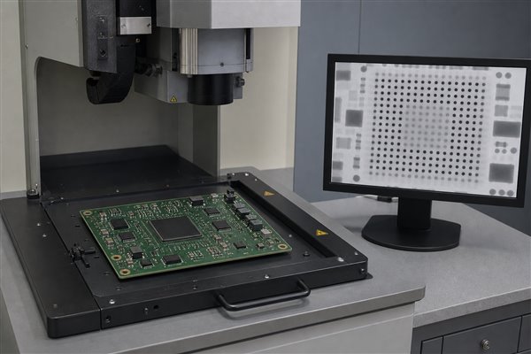
- Inspect by joint visibility. AOI can evaluate many gull-wing joints. QFN, LGA, BGA, and CSP connections may require X-ray, electrical test, boundary scan, or functional test because critical joints are hidden.
- Close the loop. Relate defects to paste, placement, reflow, footprint, board finish, component condition, and handling instead of changing one parameter without evidence.
Which IPC and JEDEC Standards Apply to IC Packages and PCB Land Patterns?
IPC documents mainly guide PCB land patterns, assembly processes, and acceptance, while JEDEC documents address semiconductor package outlines, terminology, handling, and reliability topics. The applicable revision and customer contract must be checked before a requirement is treated as mandatory.
| Reference | Primary Scope | Engineering Use | Important Boundary |
| IPC-7351 and IPC-7352 | Surface-mount land-pattern principles and current design guidance | Use IPC-7351 as a legacy framework and check IPC-7352 when establishing current land-pattern practice | IPC lists IPC-7351 as no longer maintained; use the exact package drawing and the revision required by the customer contract |
| IPC-7093 and IPC-7095 | Design and assembly guidance for bottom-termination components and BGAs | Reviews package implementation, PCB design, assembly-process, inspection, and reliability considerations | Use IPC-7093 for QFN/LGA-style bottom terminations and IPC-7095 for BGA applications; confirm the current revision |
| IPC-7525 | Stencil-design guidance | Supports aperture and stencil decisions for solder-paste printing | Device guidance, paste behavior, board design, and demonstrated process capability still control the released stencil |
| J-STD-001 | Soldered electrical and electronic assemblies | Process and workmanship requirements under the agreed product class and contract | It does not supply the component manufacturer’s package dimensions |
| IPC-A-610 | Electronic-assembly acceptance | Post-assembly acceptance criteria, including visual examples and product-class interpretation | Hidden joints may need additional methods and customer-defined evidence |
| JEDEC JEP95 registered outlines | Registered semiconductor-device package outlines | Provides standardized outline references when adopted by the component supplier | The component datasheet and orderable package drawing control the purchased part |
| J-STD-020 | Moisture/reflow sensitivity classification for plastic surface-mount devices | Supports component reflow qualification and classification review | It is not a replacement for the assembly’s measured reflow profile |
| J-STD-033 | Packaging and handling of moisture-sensitive nonhermetic solid-state surface-mount devices | Controls exposure, storage, dry packing, and recovery actions | IPC lists Revision D as no longer maintained; apply the contractual revision, component classification, and actual floor-life history |
Record the component-drawing revision, land-pattern source, assembly class or agreed acceptance criteria, X-ray or void limits, moisture controls, and required test evidence in the release package. If the drawing, standard, and purchase specification disagree, resolve the conflict before production starts.
What Limitations, Assembly Defects, and Reliability Risks Affect Each Package Type?
Every package type exchanges one advantage for another, and its dominant risks follow the terminal geometry and assembly process. Visible leads improve inspectability but can bend. Hidden lands increase density but reduce direct inspection. Fine pitch saves area but narrows printing, placement, routing, and rework margins.
- DIP: bent pins, incomplete hole fill, solder bridging, barrel damage during rework, and excessive board area.
- SOP / SOIC: bridges, opens, lifted leads, insufficient solder, polarity errors, and lead coplanarity problems.
- QFP: bent fine-pitch leads, bridging, opens, lead-to-pad misalignment, and handling damage.
- QFN: insufficient edge-joint formation, center-pad voiding, floating from excess paste, opens, shorts, and thermal-path inconsistency.
- LGA: hidden opens, uneven solder volume, warpage sensitivity, contamination, and limited rework visibility.
- BGA: head-in-pillow where a ball and paste deposit do not fully join, non-wet opens, bridging, voiding, pad cratering, warpage-related defects, and difficult fault localization.
- CSP: very narrow process margins, board-flex stress, underfill trade-offs, moisture/reflow sensitivity, and fatigue under thermal or mechanical cycling.
The operating environment can overturn an otherwise sensible package choice. Vibration, board bending, drops, thermal cycling, high junction temperature, contamination, and repeated rework stress different joints in different ways. There is no universally most reliable family; qualify the package together with the board, alloy, assembly process, enclosure, and actual load profile.
How Should Engineers Review IC Package Selection and Assembly Failures?
Review package selection before layout release, then investigate assembly failures by tracing the exact part, footprint, PCB data, process history, inspection evidence, and electrical symptom. Selection prevents avoidable incompatibilities; failure review isolates the mechanism after a defect appears.
- Define the selection requirements. Record I/O count, electrical speed, power dissipation, board-area limit, height limit, environment, inspection access, repair strategy, production volume, and approved sourcing constraints.
- Compare feasible package options. Check each candidate’s pin map, thermal path, fan-out demand, footprint availability, PCB stackup impact, assembly process, inspection coverage, lifecycle status, and total manufacturing risk before approval.
- Freeze the evidence. Record the exact part number, manufacturer, package code, lot information, board revision, BOM revision, placement data, paste, stencil revision, reflow profile, and inspection records.
- Compare source dimensions. Check the package drawing against the controlled footprint, including pin map, body size, lead span, pitch, terminal dimensions, exposed pad, solder mask, and paste layers.
- Check board manufacturability. Review pad registration, solder-mask web, via treatment, copper balance, local warpage risk, surface finish, fan-out, and stackup constraints.
- Reconstruct the assembly process. Examine paste printing, board support, placement offsets, component handling, moisture exposure, measured reflow temperatures, cooling, cleaning, and rework history.
- Use complementary inspection. Combine visual inspection, AOI, X-ray, electrical test, continuity checks, boundary scan, functional test, microscopy, cross-sectioning, or destructive dye-and-pry analysis only when each method fits the suspected failure.
- Separate symptom from cause. An intermittent signal may originate from a solder joint, via, trace, component, connector, firmware state, or test fixture. Confirm the physical failure mechanism before changing the design.
- Control the corrective action. Update the footprint, stencil, profile, handling rule, test limit, or supplier instruction through revision control, then verify the change on an appropriate build.
A useful review ends with marked package drawings, a footprint comparison, relevant X-ray or section images, test records, a confirmed failure mechanism, named corrective-action ownership, and a controlled release package. “Difficult to assemble” is not a finding; the records must show what failed, why it failed, and how the correction will be verified.
FAQs About IC Package Types
Q1: Why must the complete orderable part number be checked?
A1: A shared device name does not guarantee the same package, pin map, temperature grade, or packing option. Suffixes are manufacturer-specific and may identify body dimensions, terminal finish, reel quantity, orientation, or qualification grade. Match the complete code to the current datasheet, package drawing, approved BOM, and purchase order before releasing the footprint or substitute.
Q2: How should tape-and-reel orientation be confirmed?
A2: Confirm the supplier’s packing drawing, pin-one orientation, pocket direction, and reel feed direction. The component drawing alone may not define how the part arrives at the placement machine. Compare the packing specification with centroid rotation, feeder setup, assembly drawing, and first-article inspection. This prevents systematic rotation errors across an entire reel.
Q3: What is package coplanarity and why does it matter?
A3: Coplanarity is the variation in height among terminals that should contact the PCB during soldering. Excessive variation can leave one or more leads, lands, or balls above the paste deposit and create opens. Use the component specification for the allowable value, then consider PCB flatness, paste height, placement force, and reflow warpage before assigning the cause.
Q4: Should thermal vias be placed inside an exposed pad?
A4: Thermal vias can improve heat transfer, but their size, pitch, fill, and surface treatment must be controlled. Open vias may draw solder away from the joint or release trapped gas during reflow. Agree on via construction with the PCB fabricator and assembler, segment the paste pattern where appropriate, and verify the thermal design against the component supplier’s guidance.
Q5: Should fine-pitch package pads be solder-mask-defined?
A5: No single solder-mask strategy is correct for every fine-pitch package. Mask-defined and copper-defined pads change exposed copper geometry, mask registration sensitivity, solder behavior, and repair risk. Follow the component and land-pattern guidance, check the fabricator’s minimum mask web and registration capability, and review the complete pad array instead of applying one rule to every terminal.
Q6: How should package height and mechanical clearance be verified?
A6: Use the maximum package height and tolerance from the controlled drawing, not only the nominal 3D model. Check enclosure clearance, heat sinks, shields, connectors, test fixtures, and neighboring components. Include PCB thickness and warpage tolerances where they affect the assembly envelope. A mechanical interference review should be completed before the board and enclosure are released.
Q7: When should underfill be considered beneath a BGA or CSP?
A7: Underfill may help when drop, bending, vibration, or thermal-fatigue loads exceed the unsupported joint margin. It also changes reworkability, inspection, material compatibility, cure conditions, and stress distribution. Select it through product-level reliability analysis and qualification, not as an automatic repair for poor soldering. Confirm keep-outs and dispensing access before layout release.
Q8: How many times can an IC package be reworked safely?
A8: There is no universal safe number of rework cycles. The limit depends on component temperature exposure, moisture condition, pad integrity, laminate damage, solder alloy, warpage, cleaning, and the approved repair procedure. Record every heat cycle, inspect the site and surrounding parts, and stop when the component or PCB no longer meets the defined acceptance criteria.
Q9: Can any lead-free IC package use the same lead-free reflow profile?
A9: No; “lead-free” does not define one universal thermal limit or process window. Check the component’s declared reflow classification, package thickness, moisture sensitivity, terminal finish, and supplier limits. The assembly profile must also suit the solder paste and measured board temperatures. Verify both component exposure and solder-joint formation instead of relying on the alloy label alone.
Q10: What evidence should accompany X-ray inspection results?
A10: Retain the inspected location, image orientation, acceptance criteria, machine settings, and disposition. A single image without traceability may not show which component, board, or joint was evaluated. Link X-ray findings to visual inspection, electrical symptoms, process records, and destructive analysis when needed. State clearly which suspected defects the image can and cannot confirm.
Q11: How should an opened moisture-barrier bag be controlled?
A11: Record the opening time, ambient exposure, component moisture classification, and remaining floor life. Store, reseal, dry-pack, or bake parts only according to the applicable handling procedure and component limits. Do not reset exposure records by assumption. Maintain lot identity through kitting, return unused parts promptly, and keep humidity-indicator and desiccant evidence when required.
Q12: Can a downloaded CAD model be trusted for final mechanical release?
A12: Treat a downloaded model as a convenience file until its geometry and revision match the controlled package drawing. Check body dimensions, terminal position, seating plane, pin one, exposed pad, and maximum height. Library source names can be ambiguous, and models may omit tolerances. Approve the footprint and enclosure clearance from controlled dimensions, not appearance alone.
Need a quotation for PCB fabrication or assembly using DIP, QFP, QFN, LGA, BGA, or CSP components? Send your Gerber files, BOM, assembly drawings, and production requirements to sales@bestpcbs.com. EBest Circuit will review the package-related manufacturing requirements and prepare a quotation.