





High speed PCB design is the discipline of controlling how fast signal edges travel through a real interconnect. A successful board needs more than clean routing: the stackup, dielectric system, trace geometry, reference planes, vias, connectors, power distribution network, and fabrication tolerances must work as one electrical structure.
This guide explains the decisions that should be settled before routing, the checks that protect signal and power integrity, and the manufacturing information a PCB supplier needs. The goal is not to promote one universal spacing or length rule. It is to show how interface requirements become a controlled, testable board construction.
What Is High Speed PCB Design?
High speed PCB design begins when an interconnect can no longer be treated as an ideal wire. During a fast transition, the trace, return plane, vias, pads, connectors, and package behave as a transmission path with distributed inductance, capacitance, resistance, and dielectric loss.
The important design questions are therefore electrical and physical at the same time:
- Will the channel maintain the required characteristic impedance?
- Can return current follow the signal without crossing a plane split or large discontinuity?
- Are insertion loss, reflection, crosstalk, jitter, and skew within the interface budget?
- Can the selected material, stackup, via structure, and trace geometry be manufactured repeatedly?
- How will the finished board be tested against the released requirements?
When Does a PCB Signal Become High Speed?
A signal becomes a high-speed layout problem when its transition time is short enough for the physical interconnect delay to matter. Clock frequency alone is not a reliable boundary. A moderate-frequency clock with a sharp edge may require transmission-line treatment, while a higher-frequency but slower edge on a short connection may be less demanding.
Start with the driver rise and fall times, not only the advertised data rate. Compare the edge time with the propagation delay of the complete path, including packages, traces, vias, connectors, and cables. When the signal can encounter a meaningful impedance change before the transition has settled, reflection and return-path control become design constraints.
| Evidence | What It Changes |
| Fast edge relative to channel delay | Treat the route as a transmission line |
| Long channel or high data rate | Evaluate insertion loss and equalization margin |
| Parallel high-speed buses | Control timing, skew, coupling, and reference planes |
| Dense BGA escape | Plan layer transitions, via geometry, and return vias early |
| Low-voltage high-current ICs | Design the PDN against a target-impedance requirement |
High Speed PCB Design Guidelines
The most reliable high speed PCB design guidelines form a sequence: classify interfaces, plan placement, freeze the stackup with the fabricator, define impedance and timing constraints, route the most critical nets first, simulate where margin is uncertain, and verify the released fabrication data.
- Classify signal groups. Record interface standard, data rate, edge rate, target impedance, topology, timing limits, and expected channel length.
- Place around signal flow. Keep high-speed paths short and direct while reserving space for termination, decoupling, escape routing, and test access.
- Agree on a manufacturable stackup. Confirm laminate family, dielectric thickness, copper weight, layer order, finished board thickness, and impedance structures before final routing.
- Protect return paths. Route each critical signal over a continuous reference plane and provide a local return transition when the signal changes reference layers.
- Control discontinuities. Review connector launches, pads, neck-down sections, vias, stubs, test points, and plane voids as part of the channel.
- Verify, do not guess. Use the interface vendor’s layout guide, field-solver results, SI/PI simulation, DRC constraints, and fabrication feedback.
These high speed PCB design rules are a framework, not a substitute for the component manufacturer’s limits. A generic rule should never override a tighter PCIe, DDR, USB, Ethernet, HDMI, MIPI, SerDes, or FPGA requirement.
How Should the PCB Stackup Be Planned?
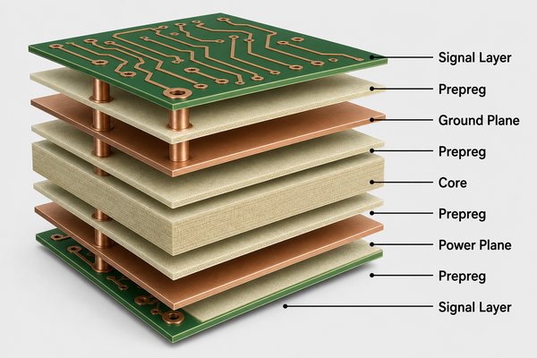
The stackup should be planned before detailed routing because it determines the available reference planes, impedance geometry, layer-transition behavior, dielectric loss, copper roughness exposure, and routing capacity. Changing it after routing can invalidate trace widths, differential spacing, propagation delay, and loss estimates.
Each critical signal layer should have a nearby continuous reference plane. Avoid placing two high-speed signal layers next to each other without a plane between them unless coupling has been evaluated. Power and ground planes placed close together can also improve high-frequency plane capacitance, but the PDN still needs a complete impedance analysis.
Do not select layer count from a generic chart alone. I/O density, escape routing, number of high-speed interfaces, power rails, board thickness, via structures, shielding needs, and cost all influence the construction. Before routing, ask the fabricator to confirm that the proposed dielectric thicknesses, copper weights, materials, and trace geometries are available and controllable.
Which Materials Work for High Speed PCB Design?
The right material is the lowest-cost system that still meets the channel’s loss, impedance, thermal, reliability, and fabrication requirements. Standard FR-4 can support many short, moderate-speed channels, while longer routes and higher Nyquist frequencies may require lower-loss laminates.
| Material Decision | Engineering Impact |
| Dk and its tolerance | Affects impedance and propagation delay |
| Df at the relevant frequency | Contributes to dielectric insertion loss |
| Copper roughness | Increases conductor loss as frequency rises |
| Glass-weave construction | Can influence differential skew in sensitive channels |
| Resin system and Tg | Affect fabrication, thermal reliability, and lead-free processing |
| Material availability | Changes achievable stackup, cost, and production continuity |
Material data must be evaluated at the frequency and test method relevant to the design. Marketing labels such as “high speed” or “low loss” do not by themselves prove that a laminate meets the channel budget. Hybrid constructions can reduce cost, but bonding, z-axis expansion, copper treatment, drill behavior, and stackup symmetry still need fabrication review.
How Do Controlled Impedance and Return Paths Work?
Controlled impedance depends on the complete transmission-line geometry: trace width and thickness, dielectric height, Dk, nearby copper, reference-plane continuity, and differential-pair spacing. The target comes from the interface specification; the final trace geometry should come from the released stackup and an appropriate field solver.
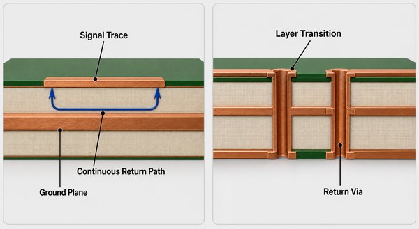
A continuous return path is equally important. High-frequency return current concentrates near the signal route on its reference plane. If the trace crosses a split, void, anti-pad field, connector discontinuity, or poorly planned reference-layer change, the current must detour. That larger loop increases inductance, radiation, coupling, and impedance disturbance.
For a deeper manufacturing view, see our impedance control PCB guide. The fabrication drawing should state the controlled nets, target values, tolerance, reference layer, coupon requirement, and any reporting requirement rather than relying on trace width alone.
What Are the Key Differential Pair and Length-Matching Rules?
Differential-pair routing should preserve the impedance, symmetry, return path, and timing budget defined by the interface. Pair spacing and length tolerance are not universal numbers; they depend on the stackup, coupling mode, data rate, receiver margin, and vendor specification.
- Route both conductors on the same layer with consistent width and spacing where possible.
- Keep reference-plane conditions and via transitions symmetrical.
- Limit unnecessary uncoupled sections around pads, vias, and connectors.
- Apply intra-pair and inter-lane tuning only to the groups that require it.
- Avoid dense serpentine tuning that creates self-coupling or moves delay into an electrically different area.
- Check skew in time, not only in physical length, when layers or materials differ.
Our differential pair PCB guide explains impedance, routing, and length matching in more detail. For final verification, inspect the complete channel rather than judging a pair only by its visual symmetry.
How Should Vias and Layer Transitions Be Managed?
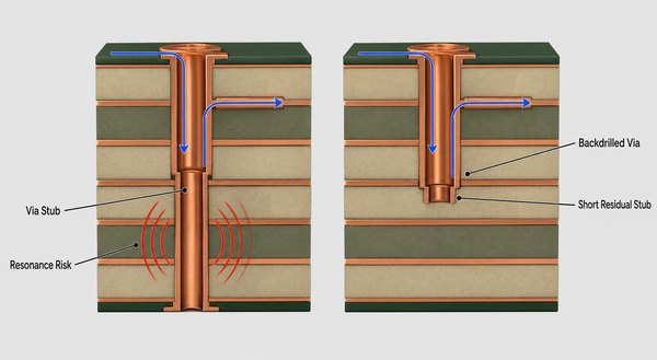
Every high-speed via transition adds an impedance discontinuity and changes the return-current path. The effect depends on barrel length, pad and anti-pad geometry, unused stub length, layer assignment, nearby return vias, and the frequency content of the signal.
Keep the number of transitions as low as the routing allows. When a signal changes layers, provide a nearby ground return via if its reference plane changes. For demanding serial channels, model the launch and review whether backdrilling, blind vias, or HDI microvias are justified. These options can improve the channel, but they also change manufacturing cost, registration requirements, and inspection needs.
Read our PCB backdrill guide before specifying stub removal. The drawing should define the drilled-from side, target layer, residual stub requirement, applicable holes, and inspection method.
How Do Power Integrity and Decoupling Affect the Layout?
Power integrity affects timing margin because high-speed receivers and transmitters rely on stable supply rails and low-noise references. The PDN should remain below its target impedance across the frequency range where the voltage regulator, bulk capacitors, MLCCs, package, and plane structure supply transient current.
Place decoupling capacitors to minimize the current loop through the capacitor pads, vias, planes, and IC power pins. Select values and packages from an impedance model rather than assuming that more capacitance always solves the problem. Anti-resonance between components, via inductance, plane spreading inductance, and package effects can create unexpected peaks.
Our high-speed PCB power integrity guide covers PDN analysis and simulation. SI and PI reviews should share the same stackup because return planes, reference noise, and power-plane cavities can affect the observed eye.
Which High Speed PCB Design Software and Simulation Tools Are Useful?
High speed PCB design software should support constraint-driven routing, stackup and impedance definition, differential pairs, length and delay tuning, design-rule checking, and manufacturable output. Simulation tools are most valuable when they answer a specific risk question rather than producing plots without acceptance criteria.
| Tool Function | Question It Should Answer |
| 2D field solver | Which trace geometry meets the impedance target? |
| Pre-layout SI simulation | Which topology, termination, stackup, and material provide margin? |
| Post-layout channel simulation | Do routing, vias, connectors, and loss meet the eye or channel requirement? |
| PI/PDN simulation | Does the supply network stay below target impedance? |
| EMI/EMC analysis | Where do return discontinuities and resonant structures create risk? |
| Manufacturing DRC/DFM | Can the released geometry be fabricated and inspected consistently? |
Use the component vendor’s IBIS or other approved models where available, and document assumptions such as material properties, copper roughness, package models, connector models, temperature, and process tolerance. A simulation is only as credible as its model boundaries.
What DFM Data Should Be Agreed With the Fabricator?
High-speed DFM should begin before final routing, not after Gerber export. The designer and PCB manufacturer must agree on the stackup and impedance construction because a small change in dielectric thickness, copper weight, material, or etching compensation can change the electrical result.
- Released stackup with material family, core and prepreg selection, copper weights, and finished thickness
- Controlled-impedance table with net class, target, tolerance, layer, and reference plane
- Critical trace, pair, spacing, delay, and skew constraints
- Via types, backdrill details, filled-via requirements, and residual-stub limits
- Coupon design, impedance test method, report format, and acceptance criteria
- Material substitution rules and the approval path for any stackup change
- Gerber or ODB++ data, drill files, netlist, fabrication drawing, and revision control
These high speed PCB design considerations also affect quotation. Low-loss laminates, tighter impedance tolerance, additional layers, HDI structures, backdrilling, extra coupons, and specialized testing may improve performance but can increase material cost, process steps, and lead time.
What Common Failures Should Be Checked Before Fabrication?
The most expensive high-speed failures are often created before fabrication data is released. A focused review should look for discontinuities and requirement gaps that a normal connectivity DRC cannot detect.
| Failure Risk | Pre-Fabrication Check |
| Reflection or poor eye opening | Review impedance changes, launches, stubs, termination, and channel loss |
| Crosstalk | Check parallel exposure, layer assignment, spacing, and reference-plane shielding |
| Unexpected skew | Compare electrical delay through layers, vias, packages, and fiber weave |
| EMI failure | Trace return-current paths and inspect splits, voids, connectors, and loop areas |
| PDN resonance | Review target impedance, capacitor models, mounting inductance, planes, and package |
| Fabrication mismatch | Freeze the approved stackup, material, impedance table, coupons, and substitution rules |
Post-layout simulation and prototype measurements should target the interfaces with the least margin. Depending on the product, verification may include TDR, impedance coupons, VNA measurements, eye diagrams, jitter analysis, bit-error-rate testing, protocol compliance testing, and functional stress tests. Our eye diagram signal integrity guide explains how to interpret eye height, width, jitter, and closure.
FAQ About High Speed PCB Design
Is every high-frequency clock automatically a high-speed PCB signal?
No. The decision depends on edge time, channel delay, interconnect geometry, and required margin. A lower-frequency signal with a fast edge and long trace may need transmission-line treatment, while a physically short route with slower transitions may be less sensitive.
Can a four-layer PCB support high-speed interfaces?
It can support some interfaces when the stackup provides continuous references and sufficient routing space. The correct layer count depends on I/O density, power rails, interface count, loss targets, via strategy, and EMC requirements. Do not select four layers only because a generic example worked elsewhere.
Are 50-ohm and 100-ohm impedance values always required?
No. They are common targets, but the correct single-ended or differential impedance comes from the interface specification. Some standards use other values. The drawing and impedance table should state the exact target, tolerance, layer, reference plane, and controlled nets.
Does every high-speed PCB require a low-loss laminate?
No. Material selection depends on channel length, Nyquist frequency, insertion-loss budget, copper roughness, temperature, reliability, and cost. Shorter channels may work on suitable FR-4 systems, while longer or faster links may need lower-loss materials.
Should all differential pairs be length matched?
Match only to the tolerance required by the interface and timing budget. Unnecessary tuning can add loss, coupling, and routing congestion. The design should distinguish intra-pair skew, lane-to-lane skew, bus timing, and absolute maximum length.
What files help a PCB manufacturer review a high-speed design?
Provide Gerber or ODB++ data, drill files, netlist, fabrication drawing, released stackup, material requirements, impedance table, critical constraints, backdrill details, coupon requirements, quantity, and revision information. Share the substitution and approval rules before material procurement.
How Can EBest Circuit Support High Speed PCB Design and Manufacturing?
At EBest Circuit, we support a manufacturable high speed PCB design from stackup and DFM review through prototype fabrication, testing, repeat production, and optional PCB assembly. Our verified capabilities include high-speed PCB, high-frequency PCB, HDI, multilayer FR-4, impedance control, AOI, electrical testing, impedance testing, microsection inspection, and copper-thickness testing.
Send your Gerber or ODB++ data, stackup, impedance table, material preference, via and backdrill requirements, quantity, and test requirements to sales@bestpcbs.com. We will review the construction and identify questions that should be resolved before material release and production.







