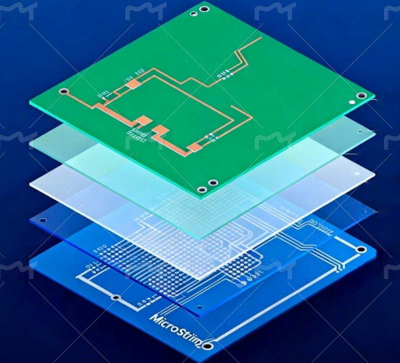
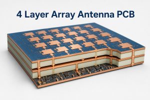
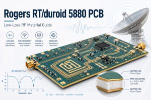
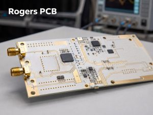
EBest Circuit provides multilayer PCB manufacturing for telecom systems, supporting standard 1–10 layer FR-4 PCBs and special multilayer constructions up to 32 layers. Our capabilities include controlled impedance, HDI structures, high-frequency materials, PCB prototyping, and turnkey assembly.
For 5G base stations, network switches, routers, and optical communication equipment, we provide custom fabrication, DFM review, component sourcing, and PCBA services. Send your specifications to sales@bestpcbs.com for a manufacturing feasibility review and quotation.
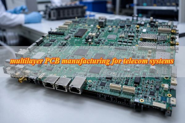
Why Choose Multilayer PCBs for Telecom Systems?
Multilayer PCBs provide the routing density, dedicated reference planes, and power distribution needed for complex telecom equipment. They accommodate high-speed interfaces, RF circuits, and dense components while keeping board dimensions manageable.
| Telecom Equipment | Why Multilayer PCBs Are Used | Main Requirements |
| 5G Base Stations | Integrate RF, digital control, and power circuits | Controlled impedance, suitable RF materials, thermal reliability |
| Network Switches | Support dense components and high-speed data channels | Low-loss signal paths, reliable vias, stable stackups |
| Routers and Gateways | Combine processors, memory, and communication interfaces | Compact construction, EMI control, continuous reference planes |
| Optical Communication Equipment | Connect optical transceivers to high-speed digital circuits | Signal integrity, connector accuracy, dielectric stability |
| Telecom Power and Control Boards | Separate control, monitoring, and power distribution | Copper thickness, thermal management, electrical insulation |
More layers do not automatically improve performance. The appropriate layer count depends on routing density, operating conditions, component packages, and electrical requirements. For high-speed and RF applications, laminate properties and stackup construction also influence signal performance.
What Are EBest Circuit’s Multilayer PCB Manufacturing Capabilities?
EBest Circuit supports multilayer PCB fabrication up to 32 layers, including fine-line circuits, high-density interconnections, heavy copper, and special laminate constructions.
| Manufacturing Parameter | Standard Capability | Special Process Capability |
| PCB Layer Count | 1–10 layers | 10–32 layers |
| Minimum Line Width / Spacing at 1 oz Copper | 4/4 mil | 3/3 mil |
| Minimum Finished Mechanical Hole | 0.20 mm | 0.15 mm |
| Minimum Laser Blind Via Diameter | 0.10 mm | Special HDI structures require review |
| Inner-Layer Copper Thickness | 0.5–5 oz | Up to 20 oz |
| Outer-Layer Copper Thickness | 1–5 oz | Up to 20 oz |
| PTH Hole Diameter Tolerance | ±3 mil | ±2 mil |
| NPTH Hole Diameter Tolerance | ±2 mil | ±1 mil |
| Surface Finishes | HASL, OSP, ENIG, immersion silver/tin | ENEPIG, hard gold, and other specified finishes |
Manufacturing limits depend on the complete PCB construction. Fine-line capabilities vary with copper thickness, while finished hole diameter, aspect ratio, material properties, and board thickness determine whether a multilayer stackup can be manufactured.
For example, a 16-layer telecom PCB combining heavy copper and fine-pitch signal routing requires separate evaluation of the copper distribution, lamination structure, and drilling requirements.
EBest Circuit supports the following specialized constructions:
- High-Layer-Count PCBs: Custom multilayer stackups with specified dielectric thickness, copper weights, and finished board thickness.
- High-Speed PCBs: Controlled-impedance structures and low-loss laminate options.
- RF and High-Frequency PCBs: Rogers, Isola, Taconic, PTFE, and other specified materials, subject to sourcing and process compatibility.
- HDI PCBs: Blind and buried vias, laser microvias, and high-density interconnections.
- Backdrilled PCBs: Through-hole stub removal for applications requiring reduced signal discontinuities.
For controlled-impedance PCBs, provide the target impedance, tolerance, layer references, dielectric requirements, and approved stackup. Our engineering team can assess whether the specified construction meets manufacturing capabilities before fabrication.
What PCB Manufacturing and Assembly Services Does EBest Circuit Offer?
EBest Circuit provides bare multilayer PCB fabrication and turnkey PCBA services, covering prototypes, small batches, and volume production.

Our services include:
- Custom Multilayer PCB Fabrication: FR-4, HDI, high-speed, high-frequency, and special-stackup PCB manufacturing.
- PCB Prototyping: Engineering samples for electrical verification, mechanical evaluation, and assembly trials.
- DFM Review: Manufacturing checks for stackups, drill structures, clearances, material compatibility, and tolerances.
- Component Sourcing: BOM review, procurement, component availability checks, and approved alternative sourcing.
- PCB Assembly: SMT, BGA, through-hole, and mixed-technology assembly.
- Inspection and Testing: Bare-board electrical testing, AOI, applicable X-ray inspection, and customer-defined functional testing.
- Volume Production: Repeat manufacturing using approved specifications, controlled revisions, and inspection requirements.
For telecom assemblies containing fine-pitch BGAs, RF connectors, shielding components, or press-fit connectors, PCB fabrication and assembly requirements are reviewed together. This helps identify potential conflicts involving board thickness, finished holes, solderability, and component placement before production.
We provide DFM guidance and manufacturing reviews based on customer-supplied designs, rather than original circuit or PCB layout design services.
What Quality Certifications and Inspection Reports Can EBest Circuit Provide?
EBest Circuit maintains quality management certifications including ISO 9001:2015, ISO 13485:2016, IATF 16949, and AS9100D. Applicable UL recognition and RoHS/REACH compliance documentation are also available according to product and project requirements.
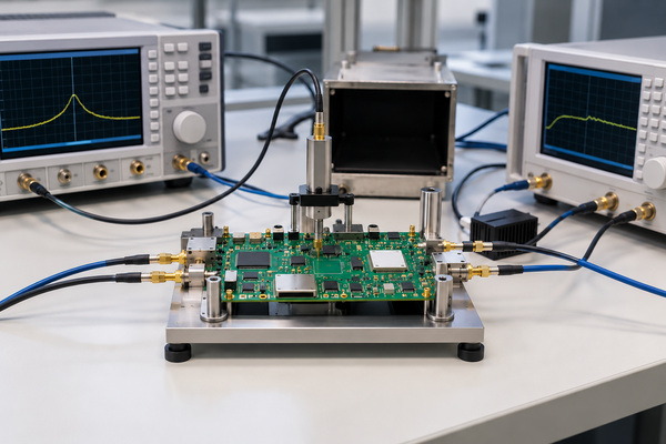
Customers can request relevant certification documents and inspection records during supplier qualification.
For multilayer telecom PCBs, quality inspection can include:
- Inner-Layer AOI: Detects conductor defects before multilayer lamination.
- Electrical Testing: Verifies continuity and isolation in finished bare PCBs.
- Microsection Inspection: Evaluates plated-hole construction, copper thickness, and internal layer structures.
- Impedance Testing: Verifies controlled-impedance structures against agreed test requirements.
- PCBA Inspection: Uses AOI and X-ray inspection where appropriate for solder joints and concealed connections.
- Functional Testing: Follows customer-defined procedures and acceptance criteria.
Electrical testing alone does not verify RF performance. If your telecom PCB requires insertion-loss, return-loss, or other RF measurements, the testing scope and acceptance limits must be agreed upon before manufacturing.
EBest Circuit also supports up to 15 years of production traceability, including relevant material, production, and inspection records according to the agreed documentation requirements.
How Long Does Multilayer Telecom PCB Manufacturing Take?
Standard FR-4 multilayer PCB prototypes can qualify for expedited manufacturing, while complex HDI, high-frequency, and hybrid-material constructions require project-specific scheduling.
| PCB Layer Count | Standard Lead Time | Fastest Service |
| 4 Layers | 10 days | 48 hours |
| 6 Layers | 10 days | 72 hours |
| 8 Layers | 12 days | 72 hours |
| 10 Layers and Above | Confirm per project | Confirm per project |
The expedited schedules apply to qualifying standard FR-4 prototypes with 0.4–1.6 mm board thickness, 0.5 oz or 1 oz copper, lead-free HASL, line width/spacing above 8 mil, and finished holes above 0.3 mm, subject to the applicable layer-count and board-size limits.
Special materials, blind and buried vias, sequential lamination, and additional testing can extend manufacturing lead time.
For PCBA orders, component availability, assembly complexity, and functional testing must also be included in production scheduling. International shipping time is quoted separately.
If you have a fixed delivery deadline, send your PCB specifications, order quantity, and required shipment date. Our team will confirm the available production schedule before order acceptance.
What Affects the Cost of Multilayer Telecom PCB Manufacturing?
Layer count, laminate selection, via structures, copper thickness, and manufacturing tolerances directly affect multilayer telecom PCB production cost. Even boards with the same dimensions and layer count can require different materials and manufacturing processes.
| Cost Factor | Manufacturing Impact |
| Layer Count and Stackup | Additional materials, layer registration, and lamination requirements |
| Low-Loss Materials | Specialized laminate sourcing, processing, and compatibility requirements |
| HDI and Via Structures | Laser drilling, blind/buried vias, sequential lamination, and backdrilling |
| Copper Thickness | Changes to etching limits, conductor geometry, and resin filling |
| Manufacturing Tolerances | Tighter control of fine lines, critical dimensions, and impedance structures |
| Order Quantity | Prototype setup, material utilization, and production planning |
| Assembly and Testing | Component sourcing, SMT complexity, inspection, and functional verification |
An 8-layer FR-4 telecom control board and an 8-layer hybrid RF PCB may have substantially different manufacturing costs because of their material, signal, and processing requirements.
When an approved design allows alternative materials or manufacturing constructions, our engineering team can assess their feasibility. Any change affecting electrical performance or approved specifications requires customer authorization.
Why Choose EBest Circuit for Multilayer Telecom PCB Manufacturing?
EBest Circuit helps telecom equipment manufacturers reduce production risks, simplify supplier coordination, and maintain consistent PCB quality across orders. With manufacturing experience dating back to 2006, we provide practical engineering and production support for complex multilayer PCB projects.
- Fewer Manufacturing Issues: Our DFM review identifies potential problems with stackups, materials, drill structures, and board thickness before fabrication, helping you avoid unnecessary revisions and production delays.
- Faster Technical Communication: Every EBest PCBA project is supported by a 1+3 technical team (PE + DFM + Process + Quality), giving you coordinated support for engineering questions, manufacturing requirements, and quality concerns.
- Simplified Purchasing and Production: PCB fabrication, component sourcing, assembly, and testing can be handled through one supplier, reducing communication gaps and the time spent coordinating multiple manufacturers.
- More Consistent Repeat Orders: Approved manufacturing files, revision control, and production traceability help maintain the required specifications across production batches and reduce the risk of unauthorized changes.
- Experienced Manufacturing Support: With 20+ years of PCB manufacturing experience, EBest Circuit helps you evaluate complex multilayer specifications, identify practical manufacturing options, and prepare projects for production.
Case Study: Multilayer PCB Manufacturing for 5G Telecom Equipment
Project Background
A telecom equipment customer required a high-frequency multilayer PCB for a 5G tower application. The board integrated RF, antenna, digital control, and power circuits, with both PCB fabrication and assembly requirements.
Requirements and Challenges
The customer required:
- Controlled impedance with a ±5% target tolerance.
- Low insertion loss and stable RF signal transmission.
- A complex multilayer stackup using suitable low-loss materials.
- Thermal management and shielding.
- Dense SMT and through-hole component assembly.
- Coordinated fabrication, assembly, and performance verification.
The challenge was to preserve the specified electrical and mechanical characteristics through PCB manufacturing and assembly.
EBest Circuit’s Manufacturing Solution
EBest Circuit reviewed the fabrication files, stackup, laminate requirements, and assembly specifications before prototype manufacturing.
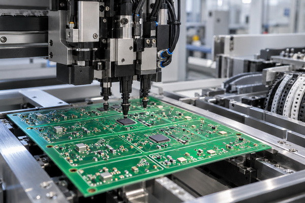
The project included:
- Material Review: Evaluating low-loss laminate requirements for the RF circuitry.
- Prototype Validation: Checking the PCB against electrical, thermal, and assembly requirements.
- PCB Fabrication and Assembly: Coordinating multilayer fabrication, SMT assembly, and through-hole assembly.
- Quality Inspection: Performing agreed inspection and verification procedures.
Project Results
The prototype met the customer’s RF, thermal, and assembly requirements and progressed into batch production. Manufacturing and assembly requirements were carried forward into production, supporting consistent quality and on-time delivery.
What Information Is Needed for a Multilayer Telecom PCB Quote?
You can request an initial manufacturing assessment with your basic PCB specifications and expected quantity. Complete fabrication files are useful for detailed engineering review but are not required for the first inquiry.
For an initial quotation, provide:
- PCB Specifications: Layer count, dimensions, finished thickness, copper weights, and preferred materials.
- Special Requirements: Controlled impedance, HDI structures, backdrilling, special finishes, or additional inspection.
- Order Details: Prototype quantity, expected production volume, delivery location, and required shipment date.
- Service Scope: Bare PCB fabrication or PCB manufacturing with component sourcing and assembly.
For detailed manufacturing approval, provide Gerber or ODB++ files, drill data, fabrication drawings, and stackup specifications. PCBA orders also require the relevant BOM, placement data, assembly drawings, and testing instructions.
Send your requirements to sales@bestpcbs.com. Our engineering team will review manufacturing feasibility, clarify technical specifications, and prepare a quotation based on your project.
Frequently Asked Questions About Multilayer Telecom PCBs
Q1: Can I specify IPC Class 3 acceptance for telecom PCBs?
A1: Yes. IPC Class 3 acceptance can be specified when required by the product. Confirm the applicable standard, revision, inspection criteria, and documentation before production.
Q2: Can different dielectric materials be combined in one multilayer PCB?
A2: Yes. Hybrid stackups can combine compatible materials, provided their electrical properties, thermal behavior, and lamination requirements are suitable.
Q3: Can I supply my own RF components for PCB assembly?
A3: Yes. Customer-supplied components can be used after confirming package compatibility, handling requirements, quantities, and incoming inspection conditions.
Q4: Are impedance test coupons required for every telecom PCB?
A4: No. They are used when controlled-impedance verification is specified. Coupon construction, target values, and acceptance criteria should be defined before fabrication.
Q5: Can EBest Circuit combine high-density BGA routing and high-current circuits on one PCB?
A5: Yes, subject to manufacturing review. Copper distribution, routing density, via structures, thermal requirements, and assembly constraints must be compatible.
Q6: Can the laminate brand be changed between production batches?
A6: Not without customer approval when the material is specified or controlled. Any proposed alternative must be evaluated for electrical, thermal, mechanical, and manufacturing compatibility.
Q7: What happens if the Gerber files conflict with the fabrication drawing?
A7: The conflicting requirements must be resolved before production. Fabrication proceeds using the confirmed file revision and approved manufacturing instructions.
Q8: Can EBest Circuit provide production lot identification for repeat orders?
A8: Yes. Production lot identification and related manufacturing records can be arranged according to the project’s traceability requirements.
Q9: Are customer-provided test fixtures or firmware needed for functional testing?
A9: They may be required. Functional testing often depends on customer-defined procedures, fixtures, firmware, and pass/fail criteria that should be confirmed before assembly.
Conclusion: Get a Quote for Your Multilayer Telecom PCB Project
Reliable multilayer PCB manufacturing for telecom systems depends on compatible materials, manufacturable stackups, controlled dimensions, and clearly defined electrical requirements. Confirming these specifications before fabrication helps prevent unnecessary production changes and quality issues.
EBest Circuit provides multilayer PCB fabrication, DFM review, prototyping, component sourcing, PCBA assembly, and inspection services for telecom OEMs and equipment manufacturers. Send your PCB specifications, quantities, and delivery requirements to sales@bestpcbs.com for a manufacturing feasibility review and quotation.