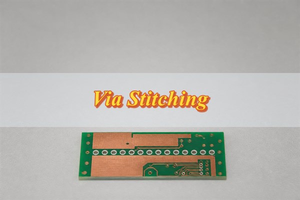
via stitching is the deliberate use of plated vias to connect copper regions on the same net across PCB layers. It is often applied to ground pours and planes so high-frequency return current can change layers with a signal. The same technique can contain board-edge fields, connect isolated copper to a reference plane, and spread heat through more copper. A useful stitching pattern is driven by current path, frequency, stackup, copper geometry, and fabrication limits—not by filling every open area with holes.
What Is Via Stitching in PCB Design?
Via stitching connects two or more copper areas that belong to one electrical net, usually GND, with repeated plated through holes. A via is itself an interlayer electrical connection; “stitching” describes how multiple vias are placed to make separated copper behave more like one three-dimensional conductor. The term overlaps with via fence, but the design task differs. General stitching distributes connections through pours or planes. A fence places a line or perimeter of vias to constrain fields near a board edge, RF trace, shield boundary, or noisy functional block.
The purpose determines whether a via is useful. A ground via beside a signal transition can shorten the return-current detour. A perimeter row can reduce the length of an electrically open board edge. Vias beneath a grounded thermal pad may also spread heat while bonding ground layers. The same-looking via grid placed far from every relevant current path may deliver little electrical benefit and consume routing area, drill capacity, and inspection effort.
What Are Stitching Vias Used For?
Stitching vias are used to control return paths, lower interplane connection inductance, contain electromagnetic fields, connect copper pours, support shielding, and sometimes improve heat spreading. These functions are related but not interchangeable, so the drawing should identify the reason for each local pattern.
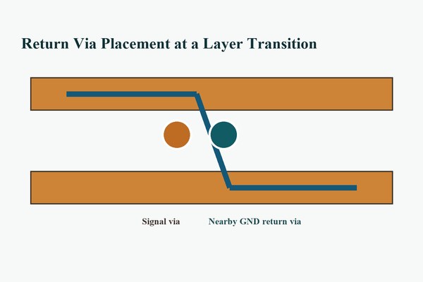
- Signal-layer transition: place a ground return via near a signal via when the signal changes reference layers. This lets high-frequency return current follow the transition instead of circulating around a remote plane connection.
- Ground-pour connection: tie top or bottom copper pours to a solid internal ground plane so the pours do not become floating or weakly connected islands.
- Board-edge containment: use a via fence along selected edges to reduce parallel-plate and edge-field propagation, especially near connectors, clocks, switching nodes, or RF structures.
- Functional shielding: surround a sensitive or noisy region with grounded copper and a compatible via fence, while checking openings, connector penetrations, and enclosure bonds.
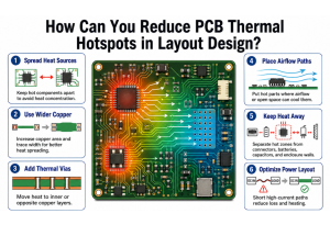
- Thermal spreading: create parallel copper paths through the board when the stitched net and land geometry also support heat flow. Thermal-via design still needs its own current, solder-wicking, assembly, and temperature analysis.
How Does Via Stitching Control the Return Current Path?
Via stitching controls return current by providing a nearby connection between the reference conductors used before and after a signal transition. At low frequency, current distribution is influenced mainly by resistance and available copper area. As edge rate increases, return current concentrates near the signal path because the lowest-impedance path is the one that minimizes loop inductance. If the signal changes layers but its reference connection is remote, the return path spreads out, enlarges the loop, and increases coupling and radiation risk.
A return via should therefore be placed according to the signal via and its reference planes, not according to a decorative grid. For a single-ended transition between layers referenced to connected ground planes, one nearby ground via may be the essential connection. For a differential transition, symmetric ground vias can reduce field imbalance, but their location must preserve pair symmetry and avoid narrowing the escape channel.
Texas Instruments interface guidance provides a device-specific example that calls for ground stitching vias symmetrically within 200 mil center-to-center of signal transition vias. This is evidence for that interface context, not a universal rule for every PCB.
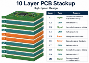
If a trace changes from a layer referenced to ground onto a layer referenced to power, a ground via alone cannot directly connect two different nets. The return-transfer method may require a carefully placed decoupling capacitor between the reference planes, a stackup change, or rerouting so the signal retains one reference. Review the complete field path rather than treating “add a via” as a universal cure.
Where and When to Place Stitching Vias?
Place stitching vias where the electromagnetic or thermal path must cross layers. Priority locations include signal transitions, relevant board edges, ground-pour necks, connector returns, shield perimeters, and unavoidable ground discontinuities. Start with the highest-risk current loops and only then fill lower-priority copper regions.
- Trace the reference: identify the plane or pour beneath each high-speed segment and note every layer change, split, slot, void, connector, and reference-plane change.
- Place transition returns: add the shortest manufacturable ground connection beside each important signal transition. For differential pairs, keep the return structure symmetric.
- Close copper bottlenecks: add connections at narrow ground necks and around antipad fields where a pour may otherwise connect through a long path.
- Define fence boundaries: place edge or shielding rows only where the field-containment objective, enclosure, and copper geometry support them.
- Recheck clearances: confirm antipads do not cut a power or ground plane into a perforated slot, and verify drill-to-copper, hole-to-hole, solder-mask, and component courtyard rules.
Avoid placing vias inside RF transmission structures, antenna keep-outs, creepage paths, flex bend zones, or assembly access areas unless the relevant design rules explicitly allow them. Also inspect via clusters near connectors and BGA escapes; a dense pattern can block routing or weaken the intended plane connection through oversized antipads.
How to Choose Via Stitching Spacing and Fence Pitch?
Via stitching spacing should be calculated from the highest frequency of concern and then checked against stackup geometry, field-containment goals, available copper, and fabrication rules. There is no single pitch that works for every digital, power, RF, or mixed-signal board.
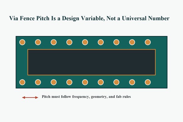
For a fence intended to suppress propagation, designers often begin with a fraction of wavelength. The wavelength in a PCB structure is shorter than in free space and depends on effective permittivity. A screening calculation can use λ = c/(f√εeff), followed by a conservative fraction such as λ/10 or λ/20.
That result is only a starting ceiling. Transitions, enclosure openings, via diameter, row offset, copper width, and the actual field mode can demand a tighter pattern. The “frequency of concern” must include fast harmonic energy associated with signal rise time, not only the data rate or clock fundamental.
For return vias beside signal transitions, wavelength pitch is not the main decision variable. Minimize the loop and keep the return connection close to the signal via while respecting antipad and routing constraints. For low-frequency copper-pour bonding, use enough vias to avoid long narrow current paths and isolated islands; simulation or impedance measurement may be more useful than a wavelength formula. For thermal or high-current stitching, calculate current sharing and temperature rise separately because current crowding, barrel resistance, copper spreading, and uneven heating prevent ideal equal sharing.
Via Size, Stackup, and Fabrication Rules to Confirm
A stitch pattern is manufacturable only when its hole, pad, annular ring, aspect ratio, drill spacing, copper clearance, and mask treatment fit the selected process. Do not copy a software default without comparing it with the fabricator’s capability table and the project’s reliability class.
| Design item | What engineering must define | What the fabricator must confirm |
| Finished hole | Electrical, thermal, and routing objective | Finished-hole tolerance and drill class |
| Pad and annular ring | Required connection and breakout risk | Minimum production annular ring after registration tolerance |
| Board thickness | Stackup and via span | Allowed through-hole aspect ratio and plating process |
| Via pitch | Return-path or shielding need | Minimum hole-to-hole and pad-to-pad spacing |
| Plane antipad | Reference continuity and impedance | Etch and registration allowance |
| Via treatment | Open, tented, filled, or capped requirement | Compatible fill, mask, planarization, and inspection route |
Dense stitching increases drill hits and can add cost or lead time, especially when it introduces a smaller drill class, via fill, sequential lamination, or stricter registration. It can also create unintended copper perforation because every nonconnecting plane needs an antipad around the barrel. Review those voids in every plane layer.
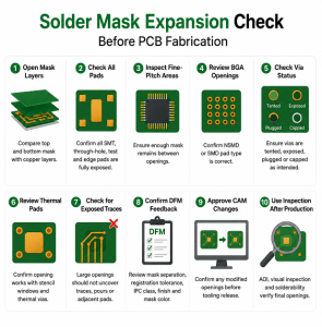
If a pattern sits beneath a component, decide whether tenting or filling is needed to control solder wicking and assembly cleanliness. A procurement package should state the via span, finished hole, pad diameter, treatment, net, and applicable acceptance class rather than relying on appearance alone.
Via Stitching for Differential Pairs and High-Speed Transitions
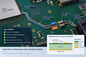
For differential pairs, stitching vias should preserve a balanced reference transition while limiting return-loop area and discontinuity. Place ground vias symmetrically around the pair where feasible and keep the signal-via geometry matched. Avoid a fence arrangement that forces one conductor to take a different escape path.
Review the transition as a three-dimensional structure. Signal-via barrel length and stubs, pad and antipad dimensions, connector launch, reference-plane separation, and nearby ground vias all influence impedance and mode conversion. Treat impedance control as part of the complete transition, not as a trace-width calculation alone. A pair can remain length matched yet become unbalanced if one signal via sees a different ground-via distance or antipad environment.
At multi-gigabit rates, use the connector or IC vendor layout guide first. Then validate the transition with a field solver, channel simulation, or test coupon when the loss and reflection budget demands it.
Do not place ground vias between the two members of a tightly coupled pair unless the transmission-line design explicitly calls for that topology. The inserted conductor changes coupling and impedance. A via fence alongside a coplanar waveguide is also part of the transmission-line geometry. Include its row offset, pitch, pad diameter, and substrate thickness in the impedance model instead of adding it after routing.
Via Stitching for High-Current and Thermal Paths
High-current and thermal via arrays may look like ground stitching, but they require separate sizing. Use current density, temperature rise, copper spreading, and assembly constraints. Increasing via count reduces the ideal parallel resistance, yet real vias do not share current equally when their approach copper, barrel length, pad geometry, or plane connection differs.
For a power path, calculate the current distribution through the complete copper system: surface trace, neck-down, pads, barrels, internal planes, and exit geometry. Check the hottest corner vias rather than dividing total current by via count. For thermal transfer beneath an exposed pad, evaluate the device datasheet pattern, copper area, board stackup, solder paste aperture, voiding risk, and whether open vias can wick solder. Filled or capped vias can improve assembly behavior but add process steps and must be explicitly specified.
Ground-stitching vias should never bridge nets or defeat an intentional isolation boundary. In safety-spaced regions, a via barrel and its internal-layer pads affect clearance and creepage. In analog layouts, stitching cannot compensate for an uncontrolled common-impedance path. The correct action may be to move the current loop, widen the return, change the stackup, or separate noisy power conversion from a sensitive reference region.
How to Add Stitching Vias in Altium, KiCad, and EasyEDA?
EDA tools can generate stitching arrays, but the operator must first select the correct net, layers, keep-outs, spacing, and via template. Automation accelerates placement; it does not decide whether the pattern supports the real return path.
- Altium Designer: define a legal via template and select the intended ground net before using the via-stitching or shielding command. Set grid or fence geometry, clearances, and object boundaries, then repour polygons and run the DRC. If Altium cannot add stitching vias or locate an area, confirm that the target polygons are poured and share the selected net. They must also overlap the chosen layers and leave enough room for the via pad plus clearance.
- KiCad: use the version-appropriate stitching or placement workflow, assign the correct net, and verify that the vias actually connect filled zones on the required layers. Refill zones and inspect connectivity; visually present holes can remain unconnected if a zone excludes them or the net is wrong.
- EasyEDA: place or array vias with the GND net assigned, then rebuild copper areas and run design-rule and connectivity checks. Confirm exported Gerber and drill files, because a screen view alone does not prove the intended plane connections.
After any automated operation, inspect three outputs: the connectivity report, the plane geometry with antipads, and the fabrication files. Remove orphan vias, vias that land only on isolated copper, and dense groups that block escapes. Lock the approved pattern or document regeneration settings so a later polygon edit does not silently remove its purpose.
How to Verify Via Stitching Before Fabrication?
Verify via stitching with connectivity, geometry, electromagnetic intent, fabrication review, and—when risk justifies it—simulation or measurement. A DRC pass proves only that encoded rules were satisfied; it does not prove the return path is short or the fence suppresses the relevant mode.
- Net and layer audit: confirm every stitching via is on the intended net and intersects useful copper on each required layer.
- Reference-path audit: trace return continuity through signal transitions, connectors, plane changes, slots, and split boundaries.
- Plane-integrity audit: view antipads on all nonconnecting layers and check that via rows do not form a slot or narrow a current path.
- Manufacturing audit: compare finished holes, pads, pitch, aspect ratio, mask, fill, and drill classes with the selected process capability.
- Fabrication-output audit: inspect Gerber or ODB++ copper, NC drill data, netlist, and a cross-section view before release.
- Risk-based validation: use 2D/3D field simulation for sensitive transitions and conduct pre-compliance EMI scans, TDR, VNA, or thermal testing when design margins are limited.
Define pass/fail evidence before testing. For a transition, that may be return loss, insertion loss, mode conversion, or eye margin. Plan EMI/EMC testing in PCBs around the applicable limit, detector, bandwidth, antenna geometry, test method, operating mode, and baseline. For thermal performance, record load, ambient condition, stabilization time, and measurement location. Without these controls, a before/after image or single spectrum peak can mislead.
Common Via Stitching Mistakes and Diagnostic Actions
The most common mistake is treating via count as performance. Diagnose the current path and the failure mechanism before adding more holes.
| Observed problem | Likely mechanism | Next engineering action |
| EMI changes little after adding a grid | Vias are remote from the dominant loop or enclosure opening | Locate the source and return path with probing or simulation; move stitching to the coupling boundary |
| High-speed transition shows excess reflection | Signal-via stub, antipad, or reference discontinuity dominates | Model the complete transition and adjust stackup, backdrill, pad, antipad, and return vias together |
| Ground pour remains isolated | Wrong net, zone priority, keep-out, or unfilled polygon | Repour, run connectivity checks, and inspect exported copper |
| Plane impedance increases near a via row | Antipads perforate or neck down the plane | Change pitch, pad stack, row position, or layer routing to restore copper width |
| Solder is pulled from a thermal pad | Open via barrels wick solder | Review via fill/cap, tenting, hole size, and paste aperture with the assembler |
| Fabricator flags drill density or annular ring | Pattern exceeds the selected process window | Use the approved drill class and spacing or request a documented process exception |
FAQs About Via Stitching
Q1: What is the difference between via stitching and a via fence?
A1: Via stitching broadly connects same-net copper across layers. A via fence is a deliberately aligned boundary used for field containment, shielding, or edge control. A fence is one application of stitching, but a general ground grid is not automatically an effective fence.
Q2: Does every signal via need a ground stitching via?
A2: No; prioritize signals whose return current changes reference layers and whose edge rate makes the discontinuity important. Low-speed signals over a continuous reference may not need a dedicated adjacent return via.
Q3: What net should stitching vias use?
A3: Most use GND, but the correct choice is the same net shared by the copper regions being connected. Never stitch different power or ground domains together unless the schematic and isolation plan explicitly requires that connection.
Q4: Can stitching vias cross a split ground plane?
A4: A ground via can only connect copper of the same ground net. It cannot repair a signal crossing between intentionally isolated nets. Reroute the signal or design an approved reference-transfer network.
Q5: Is λ/20 always the correct via spacing?
A5: No; it is only a conservative starting concept for some shielding or fence problems. The relevant frequency, effective permittivity, mode, enclosure, row geometry, and manufacturing constraints determine the final pitch.
Q6: Why is Altium unable to add stitching vias to GND?
A6: Common causes include an unpoured polygon, no overlapping same-net copper on selected layers, a wrong via template or net, and insufficient space after clearance rules. Repour, verify net assignment, and inspect the rule conflict.
Q7: Should stitching vias be tented?
A7: Tenting depends on assembly location, hole size, solder-wicking risk, cleanliness, and fabricator capability. Specify the treatment instead of assuming the solder-mask generator will choose correctly.
Q8: Can stitching vias reduce PCB temperature?
A8: They can improve heat transfer when they connect thermally useful copper, but temperature depends on copper area, barrel geometry, interface resistance, airflow, load, and component package. Validate the complete thermal path.
Q9: Do more stitching vias always reduce EMI?
A9: No; vias help only when they shorten the dominant return path or constrain the relevant field. Poorly positioned vias may add cost, consume routing space, and perforate planes without addressing the emission source.
Q10: What fabrication files should be checked?
A10: Inspect copper layers, NC drill files, netlist, solder mask, fabrication drawing, stackup, and any via-fill or cap notes. Confirm finished hole and pad definitions with the supplier before release.
Conclusion
Effective via stitching begins with a specific job: transfer high-frequency return current, connect useful ground copper, contain an edge field, support a shield, or move heat. Place vias where that path crosses layers, choose pitch from frequency and geometry rather than habit, and verify both the three-dimensional electrical structure and the fabrication outputs. A smaller, well-justified pattern can outperform a dense decorative grid while preserving routing space and process margin.
For a manufacturability review or PCB quotation, send your stackup, Gerber or ODB++ data, NC drill files, netlist, via table, impedance requirements, and via-fill notes to sales@bestpcbs.com. The engineering team can review the proposed stitching geometry against the selected board process.