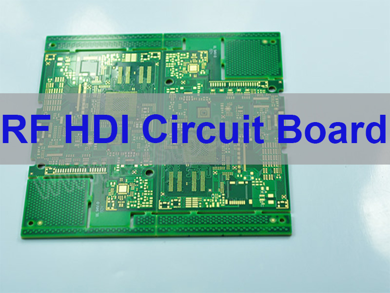
Selecting HDI PCB manufacturers in Indonesia starts with one practical question: can the supplier manufacture your released stackup repeatedly, not merely quote a board described as HDI? Filled via-in-pad, stacked microvias, sequential lamination, fine-line copper and controlled impedance require connected process controls. If one bidder includes those operations while another assumes a simpler construction or reduced testing, their prices do not represent the same product.
This guide shows what to ask before supplier approval and purchase-order release. It explains how to verify the proposed microvia and buildup structure, reconcile the stackup with drill and impedance data, define materials and inspection records, connect fabrication with fine-pitch assembly, and judge whether prototype controls can support pilot and volume production. Use the checks to obtain a reviewed stackup, named materials, a test plan and written deviations from every candidate, then compare evidence and total scope alongside price.

Which Capabilities Should You Verify in HDI PCB Manufacturers in Indonesia?
Qualify the supplier against the released interconnect structure, because an “HDI capable” label is too broad to price or manufacture a complex board safely. The same layer count can hide very different demands: one design may use a single sequential buildup, while another needs multiple buildup cycles, filled via-in-pad structures, fine routing around dense packages, or tightly controlled dielectric thickness.
- Microvia structure: identify blind-via start and stop layers, finished hole expectations, stacked or staggered construction, and whether copper-filled via-in-pad is required.
- Lamination sequence: show each core, buildup dielectric, copper layer, and sequential lamination cycle so feasibility and registration risk can be reviewed.
- Routing geometry: state the released trace width, spacing, annular features, breakout geometry, and impedance requirements rather than asking for a generic “fine line” capability.
- Material system: specify laminate family or approved alternatives, glass transition and thermal requirements where relevant, copper weights, dielectric targets, and finish.
- Via filling and planarization: define which vias must be filled and capped, because incomplete fill or poor planarity can affect both interconnect reliability and BGA assembly.
- Inspection and test: agree on electrical test, microsection locations, dimensional checks, impedance evidence when specified, and final acceptance documentation.
Do not turn these items into a capability-shopping list detached from the design. A supplier that cannot meet an unnecessary stacked-via request may still be the better source after the interconnect is simplified. Conversely, a supplier with a long capability table may still be unsuitable if it cannot explain how the proposed stackup will be built and verified at the nominated production site.
| Released Requirement | Ask the Supplier to Return | What a Useful Answer Shows |
| Via-in-pad under a fine-pitch BGA | Via span, fill type, cap-plating method and planarity acceptance | The fabricator has connected the via process to the assembly land |
| Multiple buildup layers | Numbered lamination sequence and drilling stages | The quotation includes the required sequential process rather than a simpler board |
| Controlled differential pairs | Proposed stackup geometry, tolerance and verification method | Impedance is tied to material and copper, not treated as a note on the drawing |
| Restricted material system | Exact laminate proposal and written substitution boundary | Purchasing cannot silently replace a controlled material after approval |
How Can You Confirm an Indonesian HDI PCB Manufacturer’s Real Production Capability?
The strongest evidence connects the proposed design to a documented manufacturing route, inspection plan, and production site. A certificate, equipment list, or sample photograph can support qualification, but none replaces a stackup-specific technical response.
- DFM disposition: request a marked response to the actual Gerber or ODB++ data, drill files, netlist, drawing, and stackup, including every exception that requires approval.
- Process flow: ask for the planned lamination, drilling, filling, plating, imaging, test, and inspection sequence for the quoted construction.
- Site scope: identify which legal entity and factory performs each operation and which steps, if any, are subcontracted.
- Coupon plan: define the structures used to verify plating, registration, microvia quality, and impedance when those controls apply to the design.
- Lot traceability: confirm how material batches, tooling revisions, fabrication lots, assembly lots, and inspection records remain connected.
- Change control: require approval before material, stackup, process route, fabrication site, or critical subcontractor changes.
For an initial order, compare the supplier’s written DFM response with its quotation. The layer count, buildup sequence, via treatment, material, copper, finish, test scope, and production location should agree. Resolve every deviation before purchase-order release and carry the approved answer into the fabrication traveler or equivalent controlled production record.
A useful DFM response is specific enough to close a decision. For example, it may identify that one stacked transition can be changed to staggered microvias, show the affected layers and explain the routing consequence. “Please confirm our standard process” is not equivalent because it does not disclose what will change. Keep a disposition log with the supplier question, your answer, the affected file revision and the person who approved it.
Which HDI PCB Structures Should Manufacturers in Indonesia Be Able to Build?
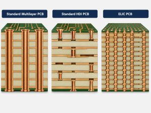
The manufacturer should support the exact buildup required by the layout, from a single microvia buildup to multistep sequential structures. A 1+N+1 construction can suit one buildup layer on each side of a conventional core, while 2+N+2 or a multistep buildup adds lamination cycles, registration demands and more opportunities for process variation. Confirm the layer transitions, not only the total layer count.
- Blind and buried vias: mark their start and stop layers in the drill data and stackup so the supplier can confirm drilling and lamination order.
- Staggered microvias: check whether the offset arrangement satisfies routing while avoiding unnecessary stacked-via complexity.
- Stacked microvias: request a process-specific reliability review because registration, plating and the interface between stacked structures become critical.
- Via-in-pad plated over: define filling, cap plating and finished planarity so the pad is suitable for the intended component.
- Filled and capped vias: identify which holes require conductive or nonconductive fill and what finished surface condition is acceptable.
Do not qualify every construction as one general “HDI level.” Create a small construction matrix for the released board. List each laser-via span, whether it is stacked or staggered, whether it terminates in a component pad, its fill and cap requirement, and the lamination stage in which it is produced. The supplier should mark each line accepted, proposed for change or unsupported. This makes one problematic transition visible before it is hidden inside a multilayer drawing.
What Should You Ask Indonesian HDI PCB Manufacturers About Microvias and Via-in-Pad?
Confirm the finished microvia geometry, laser-drilling consistency, plating condition, filling method and pad planarity against the actual layer transition. If a BGA or CSP breakout depends on via-in-pad microvias, the review should connect the finished via diameter, aspect relationship, fill and cap process to the assembly land pattern.
For stacked microvias, ask how layer-to-layer registration and the stacked interfaces are inspected. Finished-board electrical testing can find open and short circuits, but it does not replace structural evidence for plating quality or internal interfaces. Agree on suitable microsection locations and acceptance criteria before release.
During DFM, compare the microvia map with the component-placement data. Mark BGA power and ground vias, thermal paths and escape vias that cannot move without a layout change. This prevents a fabrication recommendation from being accepted in isolation and then creating an assembly, signal-integrity or thermal problem elsewhere in the design.
Ask for the acceptance method alongside the proposed process. A useful response states which features will be examined in microsection, how filled via-in-pad surfaces will be checked for assembly suitability, and how nonconforming structures will be contained. If the answer covers only nominal drill diameter, it has not addressed plating, fill, cap or finished-pad condition.
How Should You Evaluate Stackup and Sequential Lamination With an Indonesian HDI Supplier?
Review every core, prepreg or buildup dielectric, copper layer, via span and lamination cycle as one controlled construction. The proposed stackup should show dielectric thickness, copper weights, laser-via start and stop layers and the sequence used to expose each drilling step. This reveals whether the quotation and production plan reflect the same board.
Confirm material compatibility and registration controls for each cycle. Prototype and volume orders should retain the approved buildup unless a formal change is reviewed. Sending the stackup with the RFQ allows the supplier to identify feasibility issues before pricing instead of substituting an easier construction after award.
Request a returned stackup that contains more than layer names. It should identify finished thickness intent, core and buildup dielectrics, copper construction, drill stages, plated structures and the impedance geometries used for calculation. Cross-check that document against the drill legend and fabrication notes. A via shown from layer 1 to layer 3 in one file and layer 1 to layer 2 in another is a release conflict, not a shop-floor detail for the supplier to guess.
Which Fine-Line and Impedance Capabilities Matter When Sourcing HDI PCBs in Indonesia?
Ask whether the released trace and spacing can be controlled with the specified copper, laminate and impedance tolerance, rather than requesting an isolated minimum line-width number. BGA breakout, differential pairs and dense escape routing must be evaluated under the actual production conditions.
For controlled impedance, provide target values, tolerances, reference layers and the relevant geometry. Confirm how dielectric tolerance, copper thickness and etching compensation are included in the model. Where required, define impedance coupons and TDR reporting so the quotation includes the verification scope.
Ask the manufacturer to flag traces that meet the nominal design value but fall outside its stable production window after copper plating and etch compensation. The result should be a proposed geometry change or stackup adjustment tied to the affected nets. This is more useful than a marketing minimum because it evaluates repeatability under your copper and material conditions.
When reviewing the returned proposal, check that the impedance calculation and fabrication drawing use the same units, layer references and finished copper assumptions. Ask the supplier to identify which dimensions are design inputs and which will be adjusted for production. That distinction prevents a CAM compensation value from being mistaken for the finished geometry required on the drawing.
Which Materials and Surface Finishes Should Indonesian HDI PCB Manufacturers Offer?
Choose materials and finishes according to electrical loss, thermal exposure, assembly profile and component-pad requirements. High-Tg FR-4 may suit many builds, while higher-speed designs can require a qualified low-loss system. Halogen-free requirements, copper weights and permitted laminate substitutions should be stated rather than assumed.
For fine-pitch assembly, compare ENIG, ENEPIG, immersion silver or another approved finish against planarity, bonding needs, storage and assembly conditions. Require written approval before the manufacturer changes the specified laminate family or surface finish.
For every permitted alternative, record the manufacturer and material designation, the properties that must remain equivalent, and the evidence required before use. “FR-4 equivalent” is too broad for a controlled HDI build. If the project depends on loss behavior, thermal performance or a defined assembly profile, the approval should address that requirement directly rather than relying on a generic datasheet comparison.
Surface-finish review should also reach the assembly plan. Confirm the finish thickness or applicable acceptance basis, intended storage window, packaging and whether the product includes wire bonding, press-fit contacts or fine-pitch components. The supplier’s recommendation should state why the finish suits those interfaces, not merely which option is easiest to source.
What Testing Evidence Should HDI PCB Manufacturers in Indonesia Provide?
An HDI PCB manufacturer should verify microvia integrity, electrical continuity, layer registration, copper plating and controlled impedance against the released fabrication requirements. The test plan should be design-specific rather than presented as the same fixed package for every board.
- AOI and dimensional inspection: detect imaging defects and verify critical geometry at the appropriate production stages.
- Electrical test: confirm continuity and isolation against the released netlist before assembly.
- Microsection: inspect defined structures for plating, microvia and registration evidence when required by the qualification plan.
- Copper and surface checks: verify specified thickness and inspect the finished surface for assembly suitability.
- Impedance verification: use the agreed coupon and TDR method when controlled-impedance evidence is part of acceptance.
- Traceability: connect material, fabrication lot, inspection results and approved deviations to the shipped boards.
Define the records to be delivered with the lot instead of requesting “full quality documents.” A practical package may include electrical-test confirmation, impedance results where specified, material identity, final inspection status and traceability references. Microsection images or measurement data should be tied to the relevant coupon, panel or lot. This gives incoming quality teams evidence they can actually reconcile with the shipment.

Can HDI PCB Manufacturers in Indonesia Support Both Fabrication and Assembly?
Integrated PCB and PCBA support is valuable when fabrication decisions directly affect fine-pitch assembly. Via-in-pad planarity, pad finish, BGA geometry and board thickness should be reviewed before stencil design and placement begin. Connecting these decisions early reduces the risk of receiving a board that passes bare-board inspection but creates avoidable SMT defects.
For assembly, confirm component sourcing controls, stencil and solder-paste planning, fine-pitch placement, X-ray inspection where hidden joints require it, programming and functional-test responsibilities. Each inspection method should be selected because it addresses a defined assembly risk.
A combined DFM review should close the interface before either process begins. The fabrication reviewer confirms pad finish, via treatment and board geometry; the assembly reviewer confirms stencil apertures, component clearances, fiducials and inspection access. Issues should be returned in one coordinated list so the customer does not receive contradictory recommendations from separate teams.
Define the handoff outputs in the quotation: approved bare-board revision, panel format, inspection status, assembly program revision and test ownership. If fabrication and assembly occur under different internal teams or approved partners, one named project owner should control these records and coordinate failure analysis. Commercial integration without connected technical records does not remove handoff risk.
Can an Indonesian HDI PCB Manufacturer Scale From Prototype to Volume?
Yes, but only when the supplier can transfer the approved prototype construction into a controlled production process without silently changing the stackup, material, microvia route, fabrication site or inspection scope. A functional sample proves that one build worked. It does not prove that the same inputs and controls will be used for hundreds or thousands of boards.
Before approving a pilot build, compare the prototype record with the proposed production record. The supplier should return the same approved layer buildup, laser-via spans, filling and cap process, laminate designation, copper construction, surface finish and impedance method. Every prototype concession must be either closed or formally accepted for pilot; otherwise an exception can become an uncontrolled production standard.
| Scaling Check | Evidence Required Before Volume Release | Reason for the Check |
| Product identity | Matching Gerber or ODB++, drill, drawing, stackup and revision list | Prevents pilot or volume production from using a mixed data package |
| Process identity | Confirmed build site, lamination sequence, laser-drill stages, via-fill route and approved subcontracted steps | Shows whether the volume route is the route qualified by the prototype |
| Material control | Approved laminate, copper and finish with a written substitution rule | Stops purchasing changes from altering electrical or assembly behavior |
| Repeatability evidence | Pilot inspection results for microvias, registration, electrical test and impedance where specified | Tests whether the process is repeatable across panels rather than on one sample |
| Change control | Named approval path for site, material, stackup, tooling, process and test changes | Keeps later lots tied to the qualified baseline |
Volume release should follow a successful pilot review, not simply a larger purchase order. Examine lot-level defects, assembly findings, test results and approved deviations, then decide which controls and reports must accompany repeat orders. If the supplier cannot keep the prototype baseline visible in its pilot and volume documents, it has not demonstrated a reliable scaling path.
What Should You Send HDI PCB Manufacturers in Indonesia for an Accurate RFQ?
A quote-ready HDI RFQ must define the interconnect, material, acceptance, quantity, and service scope well enough for suppliers to price the same product. Sending Gerbers and asking for the “best stackup” leaves too many commercial and technical assumptions unresolved.
- Fabrication data: include Gerber or ODB++, NC drill files, IPC-356 or equivalent netlist when available, fabrication drawing, panel constraints, and revision identity.
- Stackup and vias: show layer order, dielectric targets, copper weights, blind and buried via spans, stacked or staggered structure, via-in-pad, fill, cap, and planarization requirements.
- Materials and finish: name the approved laminate or performance requirements, solder mask, legend, surface finish, finished thickness, and permitted substitutions.
- Electrical controls: identify controlled-impedance nets, target values and tolerances, test coverage, and any coupon or report requirements.
- Mechanical controls: provide board outline, cutouts, thickness tolerance, warpage requirement when applicable, edge treatment, and critical dimensions.
- Commercial quantities: separate prototype, pilot, and forecast quantities; state panel or delivery preferences without disguising an uncertain forecast as a firm order.
- Assembly scope: include BOM, centroid data, assembly drawings, package notes, approved alternates, consigned items, programming method, and functional-test requirements when assembly is requested.
- Delivery and documentation: state the ship-to destination, requested schedule, packaging needs, inspection records, certificate requirements, and importer or logistics responsibilities.
A complete RFQ allows the manufacturer to review the actual buildup, microvia structure and assembly scope before pricing. Sending these files together reduces quotation assumptions and repeated engineering questions. Ask every bidder to list deviations, subcontracted steps, tooling or test charges and quotation validity before comparing offers.
Build a bid-normalization sheet after the responses arrive. Place the proposed stackup, material, via-fill treatment, surface finish, test scope, fabrication quantity, assembly quantity, tooling and freight assumptions in separate fields. If one cell is blank, clarify it before comparing totals. This exposes whether a price difference comes from manufacturing efficiency or from missing scope.
How Should You Compare HDI PCB Manufacturers in Indonesia Beyond Unit Price?
Compare suppliers on the complete released scope: construction feasibility, DFM quality, material control, inspection, assembly support, production consistency and change management. A lower quotation may exclude via filling, impedance evidence, specified laminate, microsection work or another required operation, making it impossible to compare fairly.
| Decision Area | Evidence to Compare | Commercial Impact |
| HDI process fit | Stackup-specific DFM and confirmed via construction | Reduces redesign and quotation assumptions |
| Materials and testing | Approved material, inspection plan and required reports | Prevents scope gaps hidden inside unit price |
| Prototype response | Disposition of issues and controlled deviations | Improves pilot readiness |
| Volume consistency | Site, process, change-control and traceability records | Limits uncontrolled production variation |
| Assembly support | Board-to-assembly DFM, inspection and test ownership | Reduces handoff and rework risk |
Score each candidate against mandatory and negotiable requirements before considering price. A missing mandatory item, such as the released microvia construction or defined material, should stop direct price comparison until it is resolved. Negotiable items can be evaluated by their effect on schedule, documentation, assembly risk and total project cost. Record the reason for the award so a later buyer does not select a different scope simply because its unit price is lower.
What Mistakes Should You Avoid When Choosing an Indonesian HDI PCB Manufacturer?
Avoid any selection shortcut that makes different technical scopes look equivalent. The most common mistakes are specific and preventable:
- Comparing only PCB unit price: omitted filling, materials or testing can make a cheaper quote a different product.
- Accepting “HDI capable” without stackup review: the supplier may not have evaluated the actual buildup cycles or via spans.
- Leaving via filling undefined: bidders may price different treatments, changing both cost and assembly risk.
- Ignoring sequential-lamination cycles: quotations can be based on an oversimplified construction that cannot produce the released design.
- Assuming a prototype proves volume readiness: volume production also requires repeatable controls, frozen inputs and change management.
- Omitting impedance verification: a nominal impedance claim is not the same as an agreed coupon, tolerance and report.
- Allowing undefined material substitutions: electrical, thermal and assembly behavior can change without an explicit review.
- Failing to define inspection scope: suppliers may price different acceptance evidence even when the board description looks identical.
Why Choose EBest Circuit for HDI PCB Manufacturing?
EBest Circuit supports HDI PCB fabrication and assembly from prototype through volume production, including laser microvias, blind and buried vias, via-in-pad, sequential buildup, controlled impedance, DFM review, PCB assembly and testing. The value is not a generic capability statement; it is the ability to connect the released board structure with quotation, fabrication, assembly and inspection decisions.
- Review the HDI construction before quotation: evaluate stackup, microvia spans, via-in-pad, BGA breakout, trace and spacing, and impedance requirements so competing assumptions are identified early.
- Support complex fabrication requirements: translate laser microvias, blind and buried vias, sequential lamination, filled vias and fine-line structures into a build-specific process review.
- Keep fabrication and assembly connected: check via planarity, surface finish, BGA pads, assembly clearances and inspection access before the bare board is released.
- Control the prototype-to-volume transition: carry the approved stackup, material, via structure and accepted deviations into pilot and repeat-production records.
- Provide inspection and traceability: align electrical test, microsection, impedance verification, AOI and production records with the project’s defined requirements.
- Reduce supplier handoffs: coordinate PCB fabrication, component sourcing, SMT assembly and testing through one project workflow when the full service is requested.
Send your Gerber or ODB++, stackup, drill files, BOM, quantities and testing requirements to sales@bestpcbs.com for an HDI PCB DFM review and quotation.
FAQs About HDI PCB Manufacturers in Indonesia
Q1: What should a manufacturer return after reviewing an HDI stackup?
A1: Expect a marked DFM response, a proposed production stackup, confirmed laser-via spans, material names, copper construction and a list of deviations. The response should also identify the planned lamination and drilling stages. If the supplier returns only a price and lead time, the most important construction assumptions remain hidden.
Q2: How can you verify that microvia reliability is included in the production plan?
A2: Connect every critical microvia structure to a defined process and inspection record. Confirm drilling, plating, fill and cap requirements, then specify where microsection or other structural evidence is required. Electrical test verifies connectivity but does not by itself demonstrate the condition of an internal microvia interface.
Q3: When should stacked microvias be challenged during DFM?
A3: Challenge them when the same routing can be achieved with a staggered or simpler transition. Ask the supplier to show the affected layers and layout consequence before accepting a change. The goal is not to remove every stacked structure, but to avoid extra lamination and interface risk where it provides no necessary routing benefit.
Q4: What makes two HDI PCB quotations technically incomparable?
A4: Different stackups, materials, via treatments, test scopes or production routes make the prices incomparable. One quotation may include filled via-in-pad and impedance reports while another assumes open microvias and basic electrical test. Normalize each field and require written deviations before comparing totals.
Q5: Which quality records should be requested with an HDI PCB lot?
A5: Request only records tied to the released acceptance plan. These may include material identity, electrical-test confirmation, impedance results, final inspection status, traceability references and microsection evidence for defined structures. Each record should identify the relevant lot, panel or coupon.
Q6: How should controlled impedance be confirmed before ordering?
A6: Provide target values, tolerance, reference layers and relevant net classes, then review the supplier’s proposed geometry and material assumptions. Confirm whether coupons and TDR results are required. The calculation, returned stackup and fabrication drawing must use the same dielectric and finished-copper basis.
Q7: Which changes require approval after an HDI prototype succeeds?
A7: Require approval for changes to the fabrication site, laminate, stackup, microvia span or treatment, lamination route, critical tooling, surface finish and test method. Assembly projects should also control component-source, stencil, program and functional-test revisions where they affect the qualified product.
Q8: When does integrated HDI fabrication and assembly reduce project risk?
A8: It reduces risk when one technical workflow connects via planarity, surface finish, BGA pads, stencil design, placement, inspection and failure analysis. A single invoice is not enough. Confirm that fabrication and assembly teams share the same approved revision and that one owner coordinates cross-process issues.
Q9: Which files help an HDI manufacturer produce an accurate quotation faster?
A9: Send Gerber or ODB++, NC drill files, fabrication drawing, stackup, microvia map, controlled-impedance requirements, material and finish, quantities and required inspection records together. Add the BOM, centroid data, assembly drawings, programming and test requirements when PCBA is included.
Q10: What will EBest check during a free HDI PCB DFM review?
A10: EBest can review the released buildup, microvia transitions, via-in-pad treatment, fine-feature areas, material and finish, impedance requirements and fabrication-to-assembly interfaces before quotation. The review identifies questions and proposed manufacturing assumptions that should be resolved before the board enters production.
Send the released project package for a build-specific review and quotation. Email your Gerber or ODB++, NC drill files, stackup, microvia map, fabrication drawing and prototype or volume quantities to sales@bestpcbs.com. If assembly is required, include the BOM, centroid file, assembly drawing, programming information and test requirements. EBest will review the actual fabrication and assembly scope so the quotation identifies the proposed construction, required tests and any points that need confirmation before production.