If a laser microvia meets the drawing’s opening diameter but plating defects recur, inspect the hole wall before plating. Glass fibers can project into the hole even when its overall dimensions look right. A finished section may show an adjacent void, but it cannot always tell you whether the void started at a rough wall or developed later during metallization.
To separate those causes, compare an as-drilled witness, a witness after cleaning, and a plated section from equivalent features. Record exactly where each section was taken. That sequence gives you a more useful answer than adding a larger drill diameter to the drawing without knowing which process created the defect.
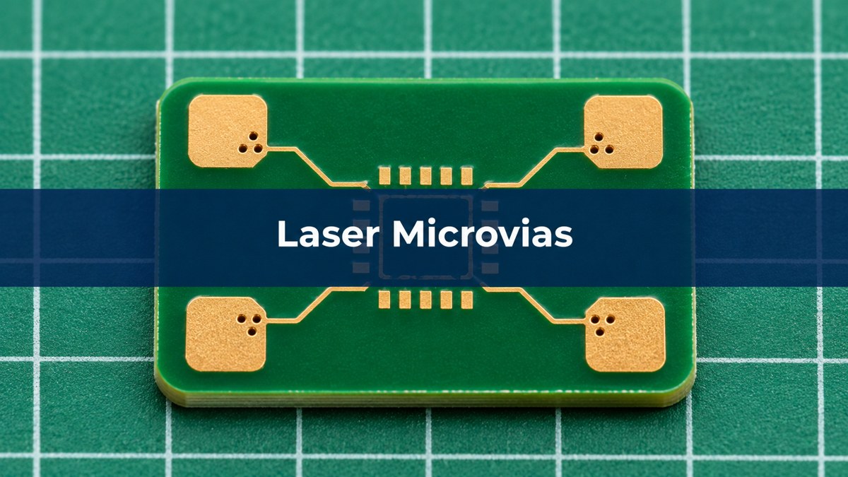
Laser drilled microvias
A laser-drilled blind microvia connects an outer or build-up copper layer to a buried target land. The laser removes material to expose the target. In glass-reinforced dielectrics, the resin and glass do not necessarily retreat by the same amount. The top opening, sidewall profile and exposed target are separate inspection surfaces.
For example, suppose a fine-pitch breakout shows repeatable plating defects on one build-up layer but not on a second layer with the same nominal opening. Start by checking which dielectric construction, laser step and cleaning sequence each group actually saw. Identical CAD openings are not evidence that the processed hole walls are identical.
Glass fiber protrusion
A protruding fiber extends from the hole wall into the cavity, beyond the nearby wall profile. It changes the local geometry where the copper layer must form. Measure the extension from the defined local wall boundary, not from the center of the hole or across the entire glass bundle. Record the largest visible value on each sampled wall and the position where it occurs.
| Parameter | What to record | Decision it supports |
| Opening and base diameters | Both locations, in µm, at an agreed section plane | Shows the overall hole shape, not local wall defects. |
| Maximum visible projection | Distance in µm from the local wall to the fiber tip | Flags a local obstruction; document the depth and side. |
| Target-land condition | Visible residue, irregularity or copper damage | Distinguishes a wall issue from a problem at the electrical interface. |
| Process stage | As drilled, after cleaning, or plated | Limits which causes the image can support. |
In a hypothetical 100 µm opening, an 8 µm projection is 8% of that reference diameter. That calculation describes the observation, not its acceptance. If the inspection plan instead defines a local diameter of 80 µm at the indicated depth, the same projection is 10% on that basis. State the denominator explicitly. The published drilling study separates protrusion, taper and target-copper damage; its research criteria are not a universal production limit.
Laser microvia aspect ratio
Aspect ratio describes a relationship between depth and a specified diameter. It does not measure roughness or projecting fibers. A smooth hole and a hole with one projecting bundle can share the same reported depth and entrance diameter. Likewise, an entrance-to-base diameter ratio describes taper, not the maximum projection.
For the example above, keep the depth and both diameters in the report, but do not use their relationship to clear the 8 µm observation. The approved drawing and inspection plan should state which dimensions and wall observations are required for release. Use the microvia aspect ratio guide for the separate dimensional check.
PCB desmear process
Cleaning prepares the drilled surface for metallization. Its purpose and capability depend on the material system and the qualified process. Resin remaining on the target land and glass projecting from the sidewall are different observations. If a change makes the hole look cleaner from above, that does not establish that the sidewall or target is ready.
Compare as-drilled and after-cleaning witnesses from the same construction. If the projection is already present after drilling, review drilling and material interactions before treating cleaning as the only corrective action. If the drilled witness is clean but the cleaned witness reveals a new wall change, investigate the cleaning step and section preparation. Use the agreed process window rather than increasing treatment until one cross-section looks better.
Microvia plating thickness
Measure copper at the locations identified by the specification and inspection drawing. A surface reading does not establish coverage at the base or around a projecting fiber. The initial conductive layer and the subsequent plating each affect the finished structure. A section should distinguish local coverage, the target interface and the interior of any copper fill.
If the team changes plating without checking the drilled wall, it can improve the average fill while leaving the difficult geometry unchanged. If the wall and base looked sound before plating but an internal void appears afterward, inspect the metallization and fill sequence before changing the laser process.
Microvia voids
A projecting fiber is a geometric feature of the dielectric wall; a void is a gap seen in the finished metal or at an interface. They may occur together, but one does not prove the other. Use the stage and location of the first observation to select the next check.
| Observation | Best next comparison | What it cannot prove |
| Fiber projects into an as-drilled wall | Check equivalent features and compare the same layer after cleaning. | It does not establish the size or presence of a plated void. |
| Gap is visible beside the plated wall | Compare unplated witness geometry and check coverage at the corresponding depth. | A single plated section cannot date the first defect. |
| Gap is inside the fill, away from the wall | Compare similar holes across the panel and review the fill process. | Not every fill void is a result of projecting glass. |
| Dark line at the target land | Inspect another section and the target before metallization. | A line alone does not identify contamination, separation or preparation artifact. |
PCB microsection analysis
Use a section plane that passes through the intended feature center for diameter measurements. If the cut is off center, the apparent opening can be smaller; it can also miss the worst wall region. Request the panel location, layer pair, section orientation and a visible scale bar rather than an isolated cropped picture.

When the projection appears on one wall only, take an additional section at the suspected region or inspect further matched witnesses. Include a known-good feature from the same construction. The IPC-TM-650 Method 2.1.1 describes microsection preparation. Use the specified product acceptance criteria separately; a well-prepared section does not by itself establish conformity.
Microvia reliability
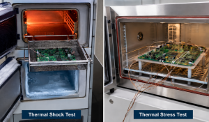
Release the corrected construction only after confirming that the wall geometry and plated structure both meet the agreed criteria. For rigid boards, check the IPC-6012 revision and class specified on the order, together with the approved drawing and inspection plan. Select coupons or boards representative of the build-up, panel positions and relevant feature sizes. If thermal or interconnect reliability testing is required, use the product’s specified protocol and include the affected layer pair in the test structure.
A room-temperature electrical pass establishes continuity at that moment, not the condition of every wall or its behavior through assembly. After a change, compare the same observation before and after the relevant process shift. Record which manufacturing layer, material and feature were validated; do not automatically extend the result to a different build-up.
Frequently asked questions
Can the entire microvia be judged from a top-down image?
No. A top view can be useful for the opening and visible target, but it may hide wall features below the opening. Use a cross-section or another approved inspection method to support claims about the sidewall.
Does a larger opening necessarily eliminate projecting glass?
No. A larger opening changes geometry, but material response to the laser and cleaning still matters. Changes also consume routing area. Compare representative witness holes before changing a board drawing.
Can the same drill qualification cover a glass-free build-up film?
Do not assume that. A glass-free layer does not have reinforcement bundles projecting into the wall in the same way, but the new material can still have residue, taper or target damage. Verify the new construction on its own terms.
Is one clean microsection enough to release all layer pairs?
Not by itself. Layer pairs can differ in dielectric, depth, laser step and plating history. Match sampling to the released construction, the agreed criteria and the risk of the feature.
Should the drawing specify a fiber projection limit?
Where it is a release criterion, agree on the measurement stage, method, dimensional reference and limit. Keep the requirement separate from the finished via diameter, and identify the controlling document and revision.
What should procurement ask for if the first article has a void?
Ask for the layer pair, panel location, calibrated section and affected lot scope. Request a comparison that separates drilled geometry from plating rather than accepting a disposition based solely on continuity.
What if the wall feature only appears after polishing?
Compare another preparation before classifying it as a process defect. Retain images from intermediate stages where available, and ask the lab to account for sectioning and polishing artifacts.
Can a tighter hole diameter tolerance substitute for a wall check?
No. It controls the stated dimension. It does not constrain local fiber geometry unless the inspection agreement specifically defines and verifies that feature.
Technical references
- Ultrashort Pulsed Laser Drilling of Printed Circuit Board Materials: Figure 1 and the accompanying definitions.
- Microvia Process Guidelines: in-process inspection of drilling and target condition.
Discuss your HDI inspection requirements
For a board inquiry, send the stackup, via layer pairs, drawing revision and annotated inspection concern to sales@bestpcbs.com. Include the applicable acceptance criteria and whether the requested evidence is for the drilled feature, plated feature or both.