Gerber to PCB conversion can recover editable physical geometry, but not the original design project automatically. The recovery scope depends on three separate questions: what the Gerber format can encode, what attributes and drill data the actual files contain, and what the chosen software can import or convert. Net, component and pin identities may already be present as Gerber attributes; footprints, schematic hierarchy and design rules still require verification or reconstruction.
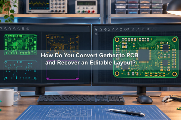
The first decision is whether conversion is necessary. A complete, internally consistent fabrication package with reliable hole and route data can often be used to manufacture the same PCB without rebuilding an editable CAD file. Reconstruction becomes necessary when the layout must be modified, migrated to another CAD system, documented, compared with a physical board or connected to a new schematic.
What Does Gerber to PCB Conversion Actually Recover?
A Gerber file describes a manufacturing layer through flashes, lines, arcs and regions. The Ucamco Gerber specification also defines object attributes: .N for a CAD net name, .P for a component reference and pin, and .C for a component reference. These can carry useful electrical identity when the exporter actually wrote them and the receiving tool preserves them. Their existence in the specification does not mean every delivered file contains them, nor does it restore the original schematic or library.
Inspect the file header and object records before estimating the work. If %TO.N,, %TO.P, or %TO.C, records are present, test whether the import tool exposes and retains those identities; otherwise infer connectivity from copper and verified holes, and use a reference netlist when available. Drill geometry may arrive as NC Drill or as dedicated Gerber drill/rout layers. The reconstructed PCB still needs engineering cleanup before becoming a controlled source.
| Information | Typical source | Recovery level | Required follow-up |
|---|---|---|---|
| Copper shapes | Top, bottom and inner-layer Gerber files | Usually recoverable as 2D geometry | Classify tracks, pads, regions and planes |
| Hole positions and sizes | NC Drill / Excellon files | Recoverable when the matching files are present | Confirm plated/non-plated status and drill spans |
| Board outline | Profile, route or mechanical Gerber | Recoverable if a closed, correctly scaled contour exists | Join segments and confirm cutouts |
| Net connectivity | Copper, drills and optional IPC-D-356 | Extractable, but not always complete | Compare inferred nets with the reference netlist |
| Footprints | Pad patterns, drill data, silkscreen, assembly data | Not preserved as library components | Rebuild and replace primitive groups |
| Schematic and design intent | Schematic, BOM, datasheets and physical-board evidence | Not stored in ordinary Gerber artwork | Recreate manually and verify pin by pin |
What Files Should You Collect Before Reconstruction?
Begin with the complete manufacturing release, not a few visible copper files. Collect every copper layer, solder mask, silkscreen, paste layers when assembly is involved, the board profile, the actual drill/rout files (NC Drill or dedicated Gerber drill layers), stackup and fabrication drawing. Keep original names and folder structure. For the Altium CAMtastic Gerber workflow described below, obtain matching NC Drill files because that workflow requires them; a Gerber drill layer is a format capability, not proof that Altium will accept it as the required drill input.
An IPC-D-356 netlist is especially valuable. It can restore meaningful net names, distinguish some vias from free pads and provide an independent connectivity comparison. A Gerber Job file, ODB++ dataset or IPC-2581 package may also preserve more manufacturing context than a traditional group of RS-274X files. Assembly drawings, pick-and-place data, BOM, board photographs and component datasheets are needed when the task includes footprints or a schematic.
| Input package | What it adds | What it still cannot prove |
|---|---|---|
| Gerber only | Layer graphics, apertures and attributes present in the files | Drill positions, component identities and complete connectivity |
| Gerber + NC Drill | Hole locations, tool diameters and a basis for via connectivity | All drill spans, plated status or original net names |
| Gerber + Drill + IPC-D-356 | Reference nets, test points and improved pad/via classification | Original footprints, schematic hierarchy and design rules |
| Gerber + assembly package | Reference designators, placements, package clues and BOM values | Guaranteed library geometry or original schematic intent |
| Original PCB project | Native objects, nets, components, rules and stackup intent | Whether the released fabrication outputs match the latest source |
Which Gerber Layers Can Be Imported Back into a PCB Editor?
The input table above describes common packages, not a format limitation. A delivered Gerber set can include dedicated drill/rout layers and .N, .P and .C attributes. Inspect the actual files before treating holes or identities as missing; then confirm that the chosen importer supports those records.
Signal copper, plane copper, solder mask, paste mask, silkscreen and mechanical artwork can be imported as layer graphics when the target tool supports those objects. The Gerber format also defines drill/rout files: flashes represent holes, draws/arcs represent slots, and separate files identify drill spans and plated status. A tool may instead require NC Drill as a separate input. Assign each imported file to the correct PCB layer; a filename extension alone is not proof of layer purpose.
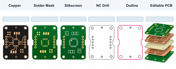
Gerber attributes may identify layer function as well as nets, components and pins, but only if present and supported by the importer. Check the actual .FileFunction and object attributes rather than assuming an X2 label guarantees usable design intelligence. Confirm how the CAM tool interprets negative polarity and split planes. Mask and paste openings help check land patterns, but they do not define a complete native footprint.
How Do You Align and Assign Imported Gerber Layers?
All files must share the correct units, coordinate format, zero suppression, origin, rotation and mirror state. A 10× scale error usually indicates a coordinate-format or unit mismatch. A top layer that appears mirrored relative to the drill data indicates an orientation error. Do not compensate by dragging individual layers until the import settings have been checked.
After alignment, assign physical order from top copper through every internal layer to bottom copper. Identify mask, paste, silkscreen and outline layers separately. Configure each through-hole, blind-via and buried-via drill span from the fabrication data. If the stackup or drill pairs are unknown, mark them unresolved rather than inferring a convenient construction.
| Observed problem | Likely cause | Check before editing geometry |
|---|---|---|
| Every layer is too large or too small by the same factor | Wrong unit or coordinate precision | Header commands, import format and known board dimension |
| Drills do not sit inside pads | Different origin, offset or drill format | Shared datum, units, zero suppression and drill tool table |
| Bottom artwork is reversed | Incorrect mirror convention | Text orientation, asymmetric features and fabrication notes |
| Only one internal layer is misaligned | Wrong source file or local offset | File revision, registration marks and layer filename |
| Outline will not form a board shape | Open or duplicated contour segments | Endpoints, cutouts, route layers and contour polarity |
How Do You Convert Copper Graphics into Editable PCB Objects?
Imported copper starts as CAM graphics: flashes, strokes, arcs and regions. The target workflow must classify these as pads, vias, tracks, polygons or copper regions. Geometry alone does not identify a component or pin; inspect .P and .C attributes before concluding that identity is absent. A large filled region may be a plane, shielding area, thermal feature or embedded conductor.
The official Altium Gerber-to-PCB workflow imports Gerber and drill data into CAMtastic, assigns layer types and order, configures drill sets, extracts a netlist and then exports to the PCB editor. After export, primitive groups still need to be replaced with footprints, polygon regions need review and repour, and drill-pair definitions may require manual recreation.
In KiCad 9.0 GerbView, load the Gerber layers, load Excellon drill files if that is the drill format supplied, use the Layers Manager to check alignment and layer identity, then choose File → Export to PCB Editor. Open the exported PCB in PCB Editor and inspect every converted object. KiCad documents this as a limited export: flashed items become vias, copper lines become track segments, non-copper lines become graphic lines, and rasterized items (often negative objects) cannot be converted. It does not promise native pads, footprints, nets or a schematic.
Can a Netlist Be Rebuilt from Gerber and Drill Data?
First inspect the delivered copper and plated-drill layers for .N net names and .P component-pin attributes. If they are absent or the tool discards them, connectivity can be inferred by tracing touching copper objects through verified plated holes and vias across the assigned stack; unnamed results need comparison against other evidence. Correct extraction depends on layer types, physical order, plane polarity and drill spans. A missing internal layer or incorrect blind-via span can merge or separate nets incorrectly.
When IPC-D-356 is available, import it before finalizing the PCB. Compare the extracted connectivity with the reference netlist and use it to restore original net names where the tool supports that operation. The Altair PollEx Gerber to PCB tutorial likewise treats IPC-D-356 as the intelligent reference used with Gerber graphics.
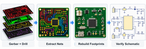
How Do You Rebuild Footprints from Gerber Data?
Group pads by repeated geometry, spacing, hole pattern, silkscreen outline and assembly reference. Then identify the component from the BOM, assembly drawing, board photograph or package dimensions in its datasheet. Build a controlled footprint with pad numbers, holes, courtyard, assembly outline and origin. Replace the imported primitive group only after the new footprint overlays the original pad and drill geometry without displacement.
Do not assume that every repeated pad array is a standard package. Connector pin numbering, polarized electrolytic capacitors, transistor pin order and bottom-contact devices are common sources of a visually plausible but electrically wrong reconstruction. The released footprint should be checked against the component datasheet and the physical board when one is available.
How Do You Reconstruct the Schematic?
The schematic is rebuilt from the verified netlist and component evidence, not converted from copper artwork in one step. Create symbols from the BOM and datasheets, assign the reconstructed footprints, and connect pins according to the extracted nets. Restore component values, part numbers, power symbols, net labels and circuit blocks from the assembly package, product documentation and physical-board inspection.
Next, compare the schematic-generated netlist with the reconstructed PCB netlist. Every mismatch needs a documented resolution. Electrical rule checking can reveal unconnected or incompatible pins, but it cannot prove that the recreated circuit expresses the original designer’s intent. Functional review and, when available, continuity measurements on a known board provide additional evidence.
| Rebuild item | Primary evidence | Verification |
|---|---|---|
| Component identity and value | BOM, marking, assembly drawing and datasheet | Cross-check reference, package and circuit position |
| Pin numbers | Datasheet and verified footprint orientation | Compare each pin with extracted copper connectivity |
| Net names | IPC-D-356, labels in documentation and circuit function | Netlist comparison and controlled naming review |
| Power hierarchy | Datasheets, decoupling network and board measurements | ERC plus voltage-domain review |
| Component blocks | Product function and repeated circuit patterns | Engineer review; do not infer undocumented behavior as fact |
How Do You Validate the Reconstructed PCB?
Validation must compare the reconstruction with the original evidence, not only check whether the new file opens. Generate fresh Gerber and drill files from the reconstructed PCB, normalize their units and origin, then overlay or XOR them against the original release. Compare copper, mask, silkscreen, outline and every drill span separately. Any unexplained difference remains an engineering deviation.
For example, suppose a reconstructed output omits a plated hole under a pad although the original copper trace and pad align. Compare the original and regenerated drill/rout layers at that pad. Check units, origin, plated status and drill span. If the source hole is present, correct the import or reconstructed via, regenerate copper and drill outputs, and compare again. Close the discrepancy only when position, diameter, classification and connectivity match the approved source. If the source hole data are missing, request the drill release or approved drawing and leave the item unresolved rather than guessing a size.
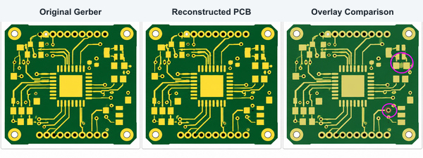
Then run PCB design-rule checks, netlist comparison and connectivity review. For example, a customer-provided IPC-D-356 file can be compared with the netlist extracted from the imported copper and again with the regenerated PCB. Record the tool version, input file revision, comparison result, approved deviations and reviewer. This creates an auditable path from the original manufacturing package to the editable design. A controlled Gerber to PCB reconstruction is accepted from this evidence, not merely because the new file opens.
| Validation stage | Controlled input | Acceptance evidence |
|---|---|---|
| Geometry overlay | Original and regenerated Gerber files | No unexplained copper, mask, legend or outline differences |
| Drill comparison | Original and regenerated NC Drill data | Tool sizes, coordinates, counts and spans agree |
| Connectivity comparison | Extracted netlist and IPC-D-356 where available | Every open, short, renamed or ambiguous net is resolved |
| Footprint review | Datasheets, BOM and pad overlay | Package, pin numbering, orientation and courtyard approved |
| Rule review | Approved stackup and manufacturing requirements | DRC rules reflect the new controlled design, not software defaults |
| Release review | Revisioned source and output package | Named approver and documented deviations |
What Manufacturing Files Should You Regenerate?
After approval, regenerate the complete fabrication package from the reconstructed source: Gerber or Gerber X2, NC Drill, fabrication drawing, stackup, drill table and any required netlist or test data. If assembly is included, also regenerate the BOM, pick-and-place file, assembly drawing, paste layers and programming or test documents. Do not combine old outputs with a revised source project unless each mixed file has been deliberately compared and approved.
Our custom PCB fabrication service reviews the controlled release as one package. For an FR4 rebuild, the FR4 PCB stackup, copper, holes, line/space, finish and test requirements must agree with the regenerated data. When assembly is required, our PCB assembly service also needs the approved BOM, placement and assembly files; these cannot be recovered reliably from ordinary Gerber artwork alone. The regenerated paste layers must also match the approved land patterns before an SMT stencil is released.
When Should You Fabricate Directly from Gerber Instead?
If the goal is to reproduce the same bare board without a design change, rebuilding a PCB project may introduce avoidable risk. A manufacturer can review a complete Gerber, drill, stackup and drawing package directly for fabrication. The source artwork remains the release authority, so no reconstructed object classification or inferred net name is required.
Convert Gerber to PCB when the layout must be edited, when a legacy product needs controlled design ownership, when an obsolete CAD format must be migrated or when the schematic and documentation need to be recreated. If critical layers, drills or dimensions are missing, pause the conversion and request better evidence. Software cannot reconstruct information that was never supplied.
Detailed Gerber-to-PCB Recovery Parameters
We check the original file headers and drawing against the import settings, then measure the same features in the reconstructed output. For example, if a Gerber header specifies millimeters and six decimal coordinate places, its coordinate grid is 0.000001 mm; this is encoding resolution, not the physical accuracy of the original board or a blanket overlay tolerance. A one-grid-unit difference in a regenerated coordinate may be rounding, but a missing hole, changed plated status or altered net is a substantive discrepancy regardless of how small a geometric tolerance is chosen. Record the exact source syntax, comparison method, measured delta and project acceptance criterion rather than selecting a universal threshold.
| Parameter | Source evidence | Decision in the recovery |
|---|---|---|
| Units and coordinate grid | Gerber MO/FS commands; drill-format header or drawing | Compare a known dimension before importing; a coordinate grid does not establish manufacturing tolerance |
| Origin and orientation | Common fiducials, asymmetric features and fabrication datum | Resolve global offset or mirroring before judging local differences |
| Layer function and polarity | .FileFunction, .FilePolarity, stackup | Separate an intentionally clear region from missing copper |
| Electrical identity | Actual .N, .P, .C records or IPC-D-356 | Reuse only identities demonstrably present and retained by the tool |
| Hole type and span | NC Drill or Gerber drill/rout layers, plated classification and stackup | Do not connect layers through an unverified blind/buried hole |
| Geometry comparison | Original and regenerated same-layer files at common origin | Report feature, coordinate and measured difference; apply the project’s approved criterion |
| Revision identity | Input package manifest and output revision | Keep the reconstructed release distinct from the original artwork |
Gerber to PCB Reconstruction vs Original PCB Source Files
| Comparison | Gerber-to-PCB reconstruction | Original PCB source project |
|---|---|---|
| Physical geometry | Recovered from released manufacturing images | Stored as native design objects |
| Net names | May survive in .N attributes or a supplied netlist; otherwise inferred and verified | Native named nets retained |
| Footprints | Rebuilt from pad patterns, available pin attributes and component evidence | Library identity and pin mapping retained |
| Schematic relationship | Must be recreated and compared | Usually linked through the project workflow |
| Design rules | Re-entered from approved requirements | Project-specific rules retained |
| Revision confidence | Depends on manufacturing-package completeness and validation | Depends on confirming that source matches the released outputs |
| Best use | Legacy recovery, migration and controlled modification | Normal design maintenance and new revision release |
Original source is preferable when it can be verified against the released manufacturing data. Reconstruction is the recovery path when that source is unavailable, not an equivalent substitute without validation. In both cases, the fabrication release should be compared with the approved design revision before production.
What Should You Send BestPCBs for a Gerber-Only Project?
Send the complete Gerber and NC Drill package, stackup, fabrication drawing, dimensions, material, copper, finish, quantity and required changes. Add IPC-D-356, ODB++, Gerber Job, BOM, pick-and-place, assembly drawing, schematic PDF, board photographs and datasheets when available. State whether you need unchanged fabrication, an editable PCB layout, a rebuilt schematic, assembly data or a complete new release package.
At EBest Circuit (Best Technology), we can review the supplied evidence, identify missing or ambiguous data, support PCB design and layout work, manufacture the approved PCB and assemble it when the required assembly package is available. For a quotation, send the files, requested deliverables, quantity and target schedule to sales@bestpcbs.com. We will define the reconstruction scope before design changes or manufacturing release.
Gerber to PCB FAQs
Can an online Gerber to PCB converter recover the complete design?
No. A converter may reproduce supported physical layers, drills and outlines, and may preserve net or component attributes when they are present and supported. It does not thereby recover the original footprints, design rules or schematic intent. Check the actual attributes and validate the output against the original manufacturing package.
Can I convert Gerber files directly into a schematic?
No direct conversion can restore a reliable original schematic from ordinary Gerber artwork alone. Rebuild the schematic from verified connectivity, BOM data, component datasheets, assembly information and physical-board evidence, then compare its netlist with the reconstructed PCB.
Do I need NC Drill files for Gerber to PCB conversion?
You need reliable hole positions, sizes, plated status and spans, but not every workflow requires the drill data to be in NC Drill format: Ucamco also defines Gerber drill/rout files. Altium’s documented Gerber-to-PCB CAMtastic workflow does require matching NC Drill files; KiCad GerbView accepts Excellon drill files for viewing. Check the actual file package and target tool before deciding whether conversion or a different workflow is needed.
Why is Export to PCB unavailable after importing Gerber files?
In workflows such as Altium CAMtastic, export depends on completing prerequisites including layer assignment, physical order, drill sets and netlist extraction. Review those items and confirm that mechanical layers and the board outline are classified correctly.
Can BestPCBs manufacture a board from Gerber without reconstructing it?
Yes, when the manufacturing package is complete, internally consistent and approved for unchanged reproduction. We still need the stackup, material, thickness, copper, finish, tolerances, quantity and applicable fabrication requirements. Reconstruction is needed when the design must be edited or documented as a new controlled source.