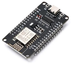
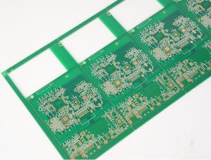
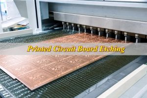
A custom wire-bondable ENEPIG PCB combines the required board structure with a controlled nickel/palladium/gold finish for qualified wire bonding and soldering. EBest Circuit manufactures these boards on FR4, ceramic and metal-core substrates to customer drawings.
EBest Circuit provides ENEPIG PCB fabrication, actual wire bonding and SMT assembly, supported by component sourcing and DFM review. Engineers and purchasing teams can coordinate the board and its interconnections through one manufacturing partner. Send your drawings and assembly requirements to sales@bestpcbs.com for a manufacturing review and quotation.
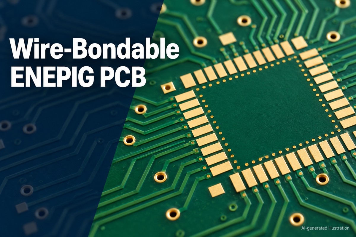
Wire-Bondable ENEPIG PCB Types Manufactured by EBest Circuit
EBest Circuit manufactures the following ENEPIG PCB types for different routing, insulation and thermal-management requirements.
| PCB Type | Construction | Typical Applications |
|---|---|---|
| FR4 / high-Tg FR4 | Single-sided, double-sided or multilayer | Chip-on-board circuits; sensor interfaces; industrial modules |
| Alumina ceramic | Al₂O₃ substrate with copper circuitry | Hybrid circuits; sensors; insulated module substrates |
| Aluminum nitride ceramic | AlN substrate with copper circuitry | Optoelectronics; heat-sensitive electronic modules |
| Metal-core | Copper or aluminum core with insulation | LED assemblies; lighting; thermal-management modules |
Substrate selection determines routing, insulation and thermal behavior. ENEPIG defines the exposed metal finish; both must suit the intended assembly process.
Custom Wire-Bondable ENEPIG PCB Manufacturing Capabilities
FR4 — standard process
The following limits apply to FR4 manufacturing. Trace width and spacing are specified at 1 oz copper; thicker copper requires a separate feature review.
| Manufacturing Parameter | Specification |
|---|---|
| Material | FR4; Tg 130–140°C, 150°C or 170–180°C |
| Layer Count | 1–10 layers; high-Tg material for ≥8 layers |
| Board Thickness | 0.4–3.5 mm with ENEPIG |
| Min. Trace Width / Spacing | 4/4 mil; 1 oz inner or outer copper |
| Min. Finished Hole | 0.20 mm |
| Copper Thickness | Inner: 0.5–5 oz; outer: 1–5 oz |
| Through-Hole Aspect Ratio | Up to 8:1 |
| Outline Tolerance | ±5 mil |
Metal-core — board construction
| Manufacturing Parameter | Specification |
|---|---|
| Material | Aluminum, copper or stainless steel |
| Board Thickness | 0.6–4.0 mm finished thickness |
| Copper Thickness | 0.5–10 oz; feature limits vary with copper thickness |
These limits apply to their respective material systems. The combination of board construction, copper features and ENEPIG finish receives a project-specific review.
Ceramic — alumina and AlN
Ceramic dimensions, metallization and tolerances depend on the selected construction. The case study below provides a detailed double-sided alumina specification; FR4 and metal-core limits do not apply to ceramic boards.
ENEPIG Plating Thickness and Surface Finish Options
EBest Circuit specifies the nickel, palladium and gold layers separately. The following two-layer FR4 order example illustrates a custom plating stack, not a universal production range.
| Layer | Thickness (μin) | Thickness (μm) |
|---|---|---|
| Nickel | 150 | 3.81 |
| Palladium | 8 | 0.2032 |
| Gold | 3 | 0.0762 |
Nickel acts as a barrier, palladium separates it from the outer gold deposit, and gold protects the bonding surface. Thickness, coverage and surface condition all matter; the finish must match the wire material, bonding method and thermal history.
Other available finishes include ENIG, OSP, HASL, immersion silver, immersion tin and hard gold, subject to the board construction. Two distinctions are important:
- Hard gold contacts. A wear-contact finish is not interchangeable with a qualified wire-bond finish.
- Nickel-free EPIG. Removing nickel changes the layer structure and requires a separate application review.
Wire Bonding and SMT Assembly Services for ENEPIG PCBs
ENEPIG fabrication and wire bonding are separate services, and EBest Circuit provides both. SMT and hybrid assembly are also available.
| Service | Process | Application |
|---|---|---|
| ENEPIG PCB fabrication | Ni/Pd/Au finishing; mask openings; bond-pad coverage | Bare-die and mixed-assembly substrates |
| Wire bonding | Device-to-substrate connections to the approved bond map | Bare-die interconnection |
| SMT assembly | Paste printing; placement; reflow soldering | SMD component assembly |
| Hybrid assembly | Coordinated SMT and wire bonding | Mixed-technology modules |
Wire material, diameter, equipment and bonding method are confirmed for each project. SMT supply options include consigned, partial-turnkey and full-turnkey assembly.
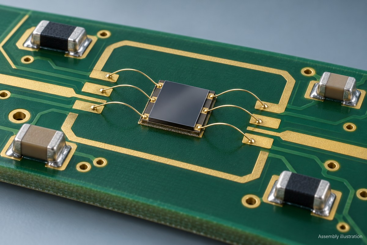
For hybrid builds, the sequence accounts for reflow exposure, flux residues, cleaning and handling. Bond pads must remain accessible and protected from solder, contamination and scratches. A compliant ENEPIG finish alone does not establish bond reliability.
DFM and Engineering Support for Wire-Bondable ENEPIG PCBs
EBest Circuit’s DFM review addresses fabrication and assembly issues before production.
- Pad geometry and access. Review pad size, spacing, mask clearance and nearby components.
- Board support. Assess thickness, flatness, panel format and clamping requirements.
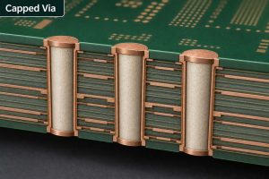
- Vias near bond pads. Identify holes, recesses or filling needs that interrupt usable surfaces.
- Finish specifications. Resolve layer thicknesses, units, coverage and alternative-finish notes.
- Assembly sequence. Review SMT, cleaning and bonding interactions.
- Drawing approval. Submit engineering questions and proposed adjustments before release.
Ceramic reviews also address copper near edges and singulation. FR4 reviews place additional emphasis on stackup and via construction.
Quality Control and Testing for ENEPIG PCBs
ENEPIG inspection covers layer thickness, pad coverage and surface condition, alongside electrical and assembly checks appropriate to the order.
| Inspection Method | Inspection Focus |
|---|---|
| Visual inspection / AOI | Pad features; mask registration; surface defects |
| Visual coverage inspection | Specified pad tops and sides; exposed copper |
| Bare-board electrical testing | Circuit continuity and isolation |
| Finish-thickness verification | Individual nickel, palladium and gold deposits |
| SMT inspection: SPI / AOI / X-ray | Paste deposits; placement; solder joints |
| Optional bond pull/shear testing | Bond integrity and failure characteristics |
Acceptance follows customer-approved drawings, process specifications and test requirements. Thickness measurement methods and suitable equipment are confirmed per order; SMT inspection applies to assembled orders. Pull/shear testing requires an agreed contractual scope, confirmed equipment capability and an approved test plan, including sampling and limits. Plating acceptance does not replace bond qualification.
Custom Wire-Bondable ENEPIG PCB Manufacturing Case Study
Project Requirements
This EBest Circuit manufacturing example uses a double-sided, 96% alumina PCB with ENEPIG-finished copper pads. The specification requires complete exposed-pad coverage, clear solder-mask openings and delivery in the customer-defined panel format. The example describes manufacturing requirements, not verified application or bond-test results.
Manufacturing Challenges & Solutions
The key challenge is coordinating finish coverage, mask clearance and panel geometry within the same build.
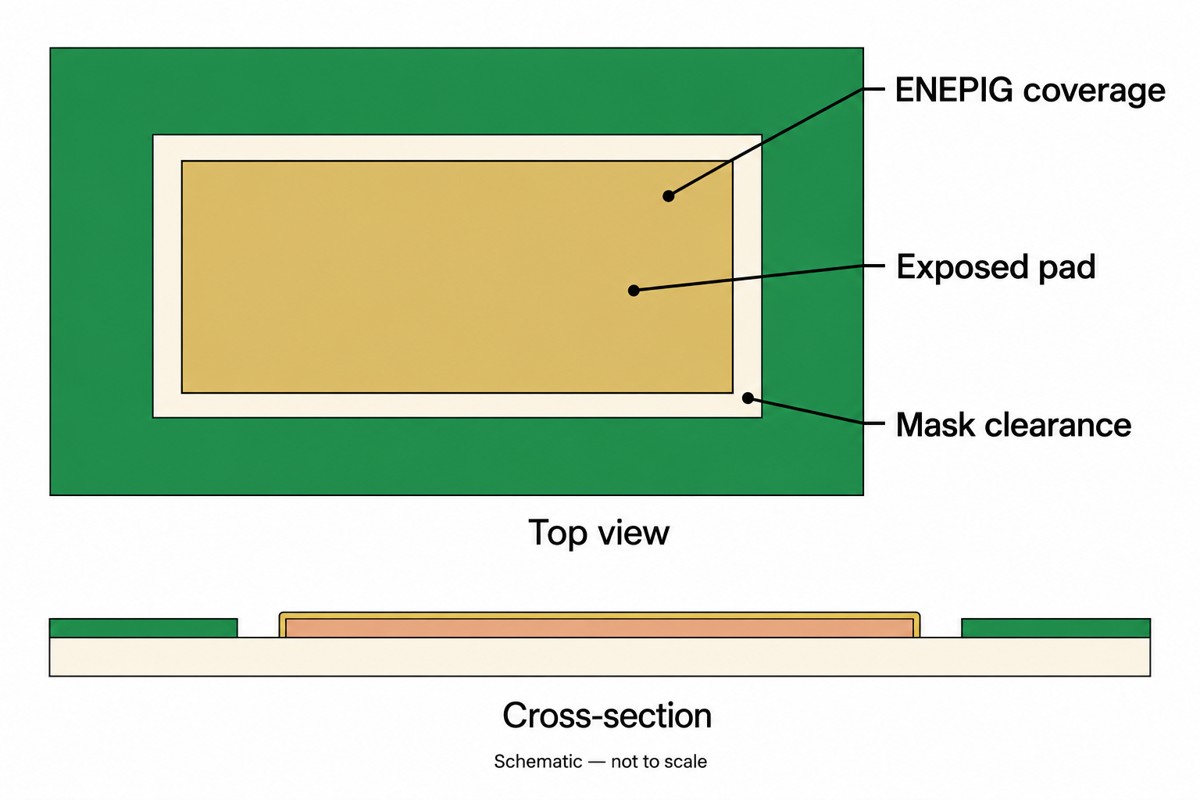
- ENEPIG Pad Coverage. Specify coverage on pad tops and all four exposed sides, with no exposed copper.
- Solder Mask Clearance. Keep green solder mask outside the specified pad area.
- Panel Dimension Control. Follow the approved layout and dimensional tolerance; add no extra holes.
- Inspection & Documentation. Align inspection with the drawing and supply the required test and inspection reports.
Key Manufacturing Specifications
| Parameter | Specification |
|---|---|
| PCB Type | Double-sided ceramic PCB |
| Substrate | 96% alumina, Al₂O₃ |
| Substrate Thickness | 1.0 mm |
| Copper Thickness | 40 ± 8 μm per side |
| Surface Finish | ENEPIG |
| Gold Thickness | >4 μin (>0.1016 μm) |
| Pad Coverage | Top and four exposed sides; no exposed copper |
| Solder Mask | Green; no mask on pads |
| Silkscreen | None |
| Controlled Panel Dimension | 114.173 ± 0.25 mm |
The panel value specifies one controlled dimension; the remaining geometry follows the approved drawing. EBest Circuit’s manufacturing requirements bring pad coverage, mask clearance and panel control together, while subsequent wire bonding remains subject to its own qualification requirements.
ENEPIG vs. ENIG for Wire Bonding
ENEPIG is often the stronger candidate for combined gold wire bonding and SMT soldering. ENIG remains suitable for many soldered assemblies and selected qualified wire-bond processes.
| Parameter | ENEPIG | ENIG |
|---|---|---|
| Layer Stack | Nickel / palladium / gold | Nickel / gold |
| Gold Wire Bonding | Common candidate for qualified gold-wire processes | Thin immersion gold is a less suitable default |
| Other Wire Materials | Wire- and process-specific qualification | Selected qualified processes |
| SMT Soldering | Compatible with controlled deposition and assembly | Widely used for soldered assemblies |
| Nickel Protection | Palladium barrier during gold deposition | Direct gold-on-nickel process control |
| Process / Cost | Added palladium step and process control | Simpler stack; generally lower processing cost |
Palladium reduces direct nickel attack during gold deposition. Neither finish guarantees bond performance by name alone; wire material, pad structure and assembly conditions remain part of qualification.
Why Choose EBest Circuit as Your ENEPIG PCB Manufacturer?
EBest Circuit combines board fabrication with the assembly services needed to turn ENEPIG substrates into populated, interconnected products.
- Fabrication plus actual wire bonding. Coordinate the board finish and wire connections with one manufacturing partner.
- Multiple substrate platforms. Match FR4, alumina, AlN or metal-core construction to the design.
- Detailed finish control. Specify individual metal layers, pad-side coverage and mask clearance.
- Engineering support before production. Address pad access, via placement, panel handling and assembly sequence early.
- Flexible assembly supply. Combine SMT with consigned, partial-turnkey or full-turnkey sourcing.
- Coordinated production records. Keep approved files, inspection requirements and work-in-progress updates connected.
How to Get a Quote for Wire-Bondable ENEPIG PCBs?
Send your files to sales@bestpcbs.com, identifying whether you need bare boards, wire bonding, SMT or a combined build.
- PCB data. Gerber or ODB++, drill files, fabrication drawing and stackup.
- Finish requirements. Ni/Pd/Au limits, applicable pad areas and specified standards or revisions.
- Bonding details. Device information, bond map, wire material and diameter, method and loop constraints.
- SMT data. BOM, placement data and assembly drawing.
- Order requirements. Quantity, testing, reports, packaging and target delivery date.
If specifications are still being developed, send the available files and application requirements for engineering review.
FAQs About Wire-Bondable ENEPIG PCB Manufacturing
Can I order bare boards for bonding by another supplier?
Yes. Include the downstream bonding requirements so the supplied pads and finish can be reviewed against that process.
Can FR4 and ceramic boards use the same ENEPIG specification?
Possibly. Substrate stiffness, thermal behavior, copper construction and fixture support can change bonding conditions even with identical finish layers.
Does a thickness report prove wire bondability?
No. Thickness data does not establish surface cleanliness, adhesion or actual bond performance. Qualification must address the wire and assembly process.
Can one bond-pull limit apply to every assembly?
No. Limits depend on wire diameter, bond geometry and product requirements. Failure location also affects interpretation.
What affects custom ENEPIG project lead time?
Substrate availability, board complexity, plating, component sourcing and qualification scope. EBest Circuit confirms the schedule after reviewing files and material status.
Need a Reliable Manufacturer for Your Wire-Bondable ENEPIG PCB?
EBest Circuit connects custom fabrication, actual wire bonding and SMT assembly with DFM support. From Ni/Pd/Au specifications to pad access and inspection planning, our team addresses the manufacturing details that affect your build.
Send your Gerber files, bonding requirements and quantities to sales@bestpcbs.com for a manufacturing review and quotation.