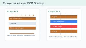
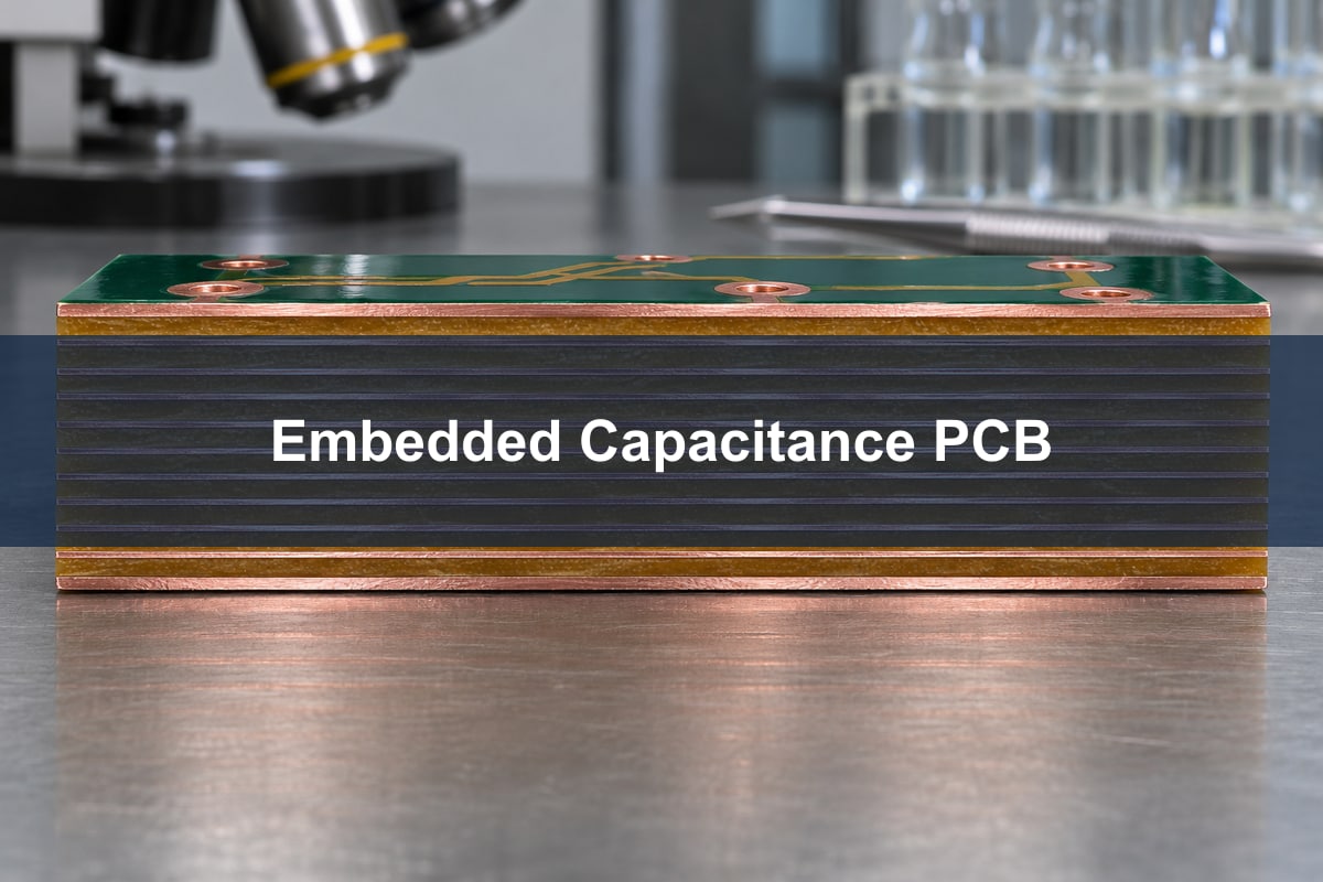
An embedded capacitance PCB uses overlapping conductors separated by a dielectric to provide capacitance inside the stackup. A closely spaced power and ground pair can help at high frequencies, but its available capacitance depends on overlap area and dielectric thickness. Keep discrete capacitors where the power rail needs more charge storage or frequency coverage.
embedded capacitance pcb
Distributed plane capacitance comes from the electric field between the planes. It differs from burying a finished discrete capacitor inside the board. The first approach spreads capacitance across copper area; the second uses a component at a particular location and needs a different fabrication and verification plan.
embedded capacitance material
Read the supplied material grade, dielectric thickness tolerance, effective permittivity and test conditions together. A thinner dielectric may provide more capacitance per area, but it also changes isolation, process handling and cost. Do not specify high permittivity without checking whether the proposed layer will also serve as a controlled reference for signals.
pcb power plane capacitance
Count the area where the intended two nets actually overlap. An unrelated copper island does not belong in the same total. Split planes and voids can cut the effective area and force a current detour. Start from the final layout rather than multiplying the entire board outline by a supplier’s capacitance density.
parallel plate capacitance formula
For an ideal approximation, C = ε₀ εᵣ A/d. With assumed εᵣ = 4, A = 20 cm² and d = 25 µm, the estimate is 2.83 nF. With the same material and area at 50 µm, the estimate falls to 1.42 nF. This ignores fringing, dispersion, losses and distributed resonance. It is not a measured value or a release specification.
| Variable | Example | Use actual |
| Overlap area | 20 cm² | Released plane artwork |
| Dielectric thickness | 25 µm | Pressed thickness |
| Relative permittivity | 4, assumed | Grade and test data |
| Ideal capacitance | 2.83 nF | Model and verify |
pcb decoupling capacitor
Embedded plane capacitance vs discrete capacitors
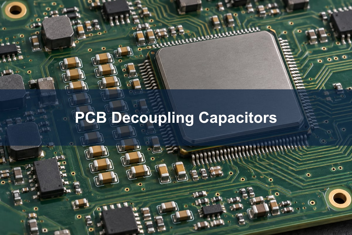
Compare each option at the load and over the relevant frequency range. A discrete ceramic capacitor can offer greater nominal capacitance, but pads, vias and placement add connection inductance. A plane pair does not eliminate the inductance between the load pins and the plane.
| Option | Useful for | Verify |
| Close plane pair | Distributed high-frequency response | Overlap, access and modes |
| Local ceramic capacitor | Charge near a device | Bias derating and mounting |
| Bulk capacitor | Slower load changes | Regulator and transient response |
pcb decoupling capacitor placement
Start from the power pin and return pin, not from the empty area closest in the placement view. Compare the full current loop into the layer pair and into the discrete capacitor. Check via placement, shared neck-downs and the return plane. A physically close capacitor with a long return loop can deliver less useful high-frequency decoupling than expected.
pcb power distribution network
Check rail impedance and load response before removing parts. Simulate the regulator, bulk and local capacitors, connections and planes over the relevant range. Changing capacitance can move peaks as well as lower impedance in some bands. See the PDN antiresonance guide for interpreting an unexpected peak.
pcb plane capacitance calculator
Use the calculator for a feasibility estimate, then compare it with measurement. In the example, even doubling the estimate would not by itself justify removing a larger capacitor at a device. Test impedance at representative load access points and verify transient droop under defined load changes. Use the same observation point when comparing the baseline with the thin-plane design.
FAQ
Does the total board area count?
No. Count copper overlap for the specific rail and its reference. Voids and isolated islands can substantially reduce usable overlap.
Can embedded capacitance replace bulk capacitors?
Generally not on the basis of geometry alone. Bulk capacitors serve a different charge and frequency range; verify regulator stability and measured load response before changing them.
Does thin dielectric guarantee lower impedance at every frequency?
No. Plane dimensions, access inductance and resonances can dominate certain frequencies. Measure or model the loaded network.
Does the formula give usable capacitance at any frequency?
No. It treats the geometry as an ideal lumped capacitor. Use a distributed model or appropriate measurement where propagation and resonances matter.
Does permittivity have to be the same for every layer?
No. Check the assigned material and test conditions per layer. A value from another laminate is not a substitute for the actual construction.
What should go into the fabrication request?
Include the approved material grade, thickness tolerance, layer order, reference nets and any coupons or electrical verification requirements.
References
Analog Devices: Decoupling Continued.
Send the proposed stackup, rail targets and routing layers to Best Technology for fabrication review.