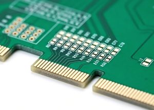
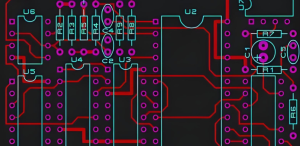
Place PCIe AC coupling capacitors only after checking which part of the link is responsible for each transmit path. Then place the two parts as a matched pair and verify their pad transitions in the actual stackup. A capacitor can be correct in the schematic and still introduce an avoidable discontinuity on the board.
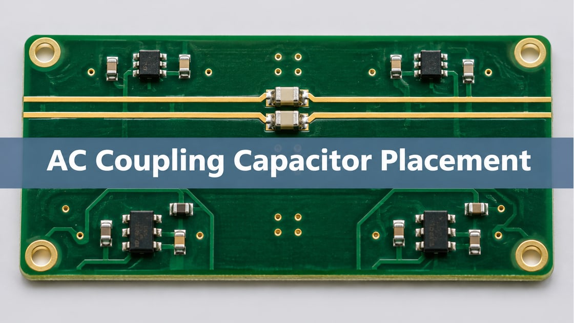
PCIe AC Coupling Capacitor Placement
Start with the platform’s channel drawing, not a rule such as “always next to the transmitter.” The transmit path tells you which lane needs coupling; physical position depends on the device and topology. Confirm which board or module provides the series parts and whether the device already integrates coupling.
Consider a hypothetical endpoint on an adapter connected to a host through a slot. Mark host transmit and endpoint transmit as separate paths. A placement decision that is correct for one direction does not automatically assign the parts in the reverse direction.
AC Coupling Capacitor for PCIe
A series coupling capacitor blocks DC while allowing the changing signal to reach the receiving path. It is not the same part as a supply bypass capacitor or a capacitor that links reference planes. On a differential lane, the approved coupling arrangement must be implemented on both conductors.
| Review item | What to verify |
| Transmit ownership | Host and endpoint paths traced separately |
| Existing series parts | On-device, adapter, or host implementation |
| Placement | Topology-specific vendor guidance |
| Part geometry | Same approved launch on both conductors |
Check the schematic against the actual channel and bill of materials. Do not add a second pair simply because a connector sits between boards.
PCIe AC Coupling Capacitor Value
Choose capacitance from the applicable platform or device documentation. TI’s PCIe Gen 5 layout note discusses a 75–220 nF range and describes 220 nF as typical in its context. Those values do not override requirements for a specific component, topology or implementation.
Check approved value, tolerance, package, voltage and the relevant high-frequency model together. A nominal capacitance match does not prove two components behave the same through their mounting geometry and parasitics.
AC Coupling Capacitor Size
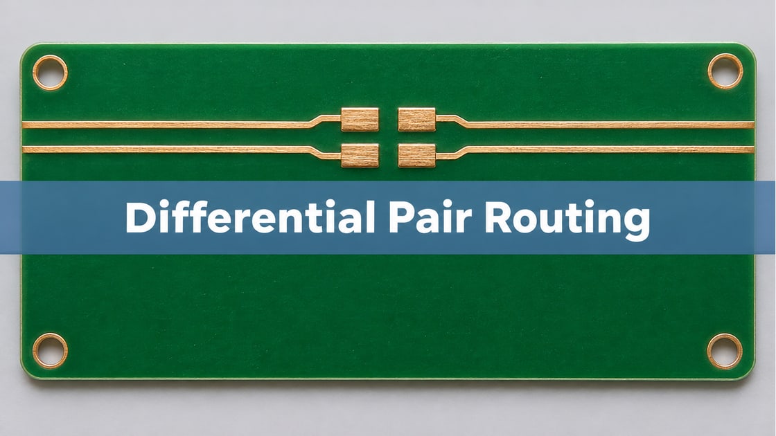
Compare the solder land with the controlled trace before selecting a package. In TI’s illustrative Gen 5 layout, a 12 mil pad is wider than a 5–7 mil trace. At an illustrative 6 mil trace width, the pad is twice as wide. That ratio is a geometry warning, not a formula for the resulting impedance.
| Placement option | Potential benefit | What to confirm |
| Smaller approved package | Smaller pad transition | Assembly and component limits |
| Existing larger footprint | Established assembly process | Modeled discontinuity is acceptable |
| Staggered pair | Fits a crowded area | Both paths still have comparable electrical response |
Differential Pair Routing Guidelines
Make the two capacitor launches geometrically comparable. Use matching footprints, equivalent approach and exit routes, and comparable vias and reference environments. Avoid adding a jog or changing layers on one conductor just to align both components visually.
If routing forces a stagger, compare the actual two-path electrical response rather than assuming a neat centerline layout compensates for it. Keep nearby copper, neckdowns and return geometry in the model.
Differential Pair Impedance
A wider mounting pad can create a local impedance dip. The depth of that dip depends on the dielectric, pad, neighboring conductor and reference plane. A small package or an engineered transition can reduce the discontinuity, but neither automatically proves the channel is within budget.
Model the footprint and launch together, and compare the result with the channel’s permitted impedance and loss behavior. Use the final land pattern, not only the package body dimensions or the nominal routed trace impedance.
PCB Return Path
Preserve the intended return path. Some platform notes use a localized reference-plane void under the capacitor launch to reduce excess capacitance. Treat that as a stackup-specific design choice. Do not cut a long slot beneath the pair or transfer the same void to a board with different layers without checking the effect.
Compare an intact reference and the proposed local relief in the actual stackup if the device guidance permits. Include both conductors and surrounding geometry. If local impedance improves but conversion or return-path behavior worsens, revise the transition instead of approving it on a single result.
PCIe Gen 5 Layout Guidelines
Release the design when ownership, capacitance, placement and both electrical paths have been checked against the approved platform. For the hypothetical adapter, verify both transmit directions, then compare the matched footprint against the actual connector and stackup. Save the channel model and the intended verification method with the board revision.
Use the Best Technology PCIe routing guide for the wider channel constraints. A link that trains on one bench sample is useful evidence, but it is not a substitute for the margin or compliance tests required for the product.
Frequently Asked Questions
Do PCIe coupling capacitors belong next to the transmitter?
The transmitter identifies the path that needs the approved coupling arrangement. It does not create a universal physical placement rule. Check the platform topology and device layout guidance. A chip-to-chip path and a chip-to-connector path can have different recommended locations for the same function.
What if both boards already contain series capacitors?
Trace the channel and confirm whether the parts are intended to operate together. Two series capacitors change the effective coupling behavior, so do not leave both simply because each board uses a familiar reference design. Resolve ownership against the approved host, adapter and endpoint requirements.
Can I place one capacitor farther along the pair?
Only if the resulting channel still passes the applicable electrical checks. The location difference can change how the discontinuities interact. Compare the complete launch, return environment and differential response rather than treating matched copper length or identical component values as sufficient evidence.
Is 0201 always the best package?
No. A smaller package can reduce the pad transition, but it must be available in the approved electrical value and suitable for the assembly process. Use the actual mounting land and model. A different package is acceptable only if the electrical and manufacturing requirements are met.
Does a plane void always improve the channel?
No. A controlled local void can help a particular capacitive pad transition, but a larger or poorly placed opening can disturb the return path. Follow the device guidance and compare the geometry in the actual stackup. Do not apply a blanket cutout underneath the entire lane.
Can an AC coupling capacitor repair a bad reference-plane transition?
No. The series component has a different function from managing a signal’s return path. The pad and nearby vias must still have a suitable reference environment. Check the reference-plane transition and coupling launch independently, then evaluate their combined effect in the complete channel.
What should I check after a PCIe link trains successfully?
Confirm the expected lane width and operating speed, then follow the platform’s margin and validation plan across required conditions. Keep the channel model, device settings and assembly revision with the results. One successful training event does not prove every lane and product condition has adequate margin.
What files help with a capacitor placement review?
Send the transmit ownership diagram, schematic, package and land pattern, final stackup, and both conductors around the capacitor. Include connector and via details plus any proposed plane relief. That makes it possible to compare the two launches instead of judging the placement from a cropped image.
References
- Texas Instruments: High-Speed PCB Layout for PCIe Gen 5
- NXP AN11082: PCB Design and Layout Guidelines
Discuss Your PCB Requirements
For a Best Technology fabrication review, send the PCIe stackup, capacitor footprint and paired route geometry to sales@bestpcbs.com. Mark the connector transitions and any localized reference-plane voids.