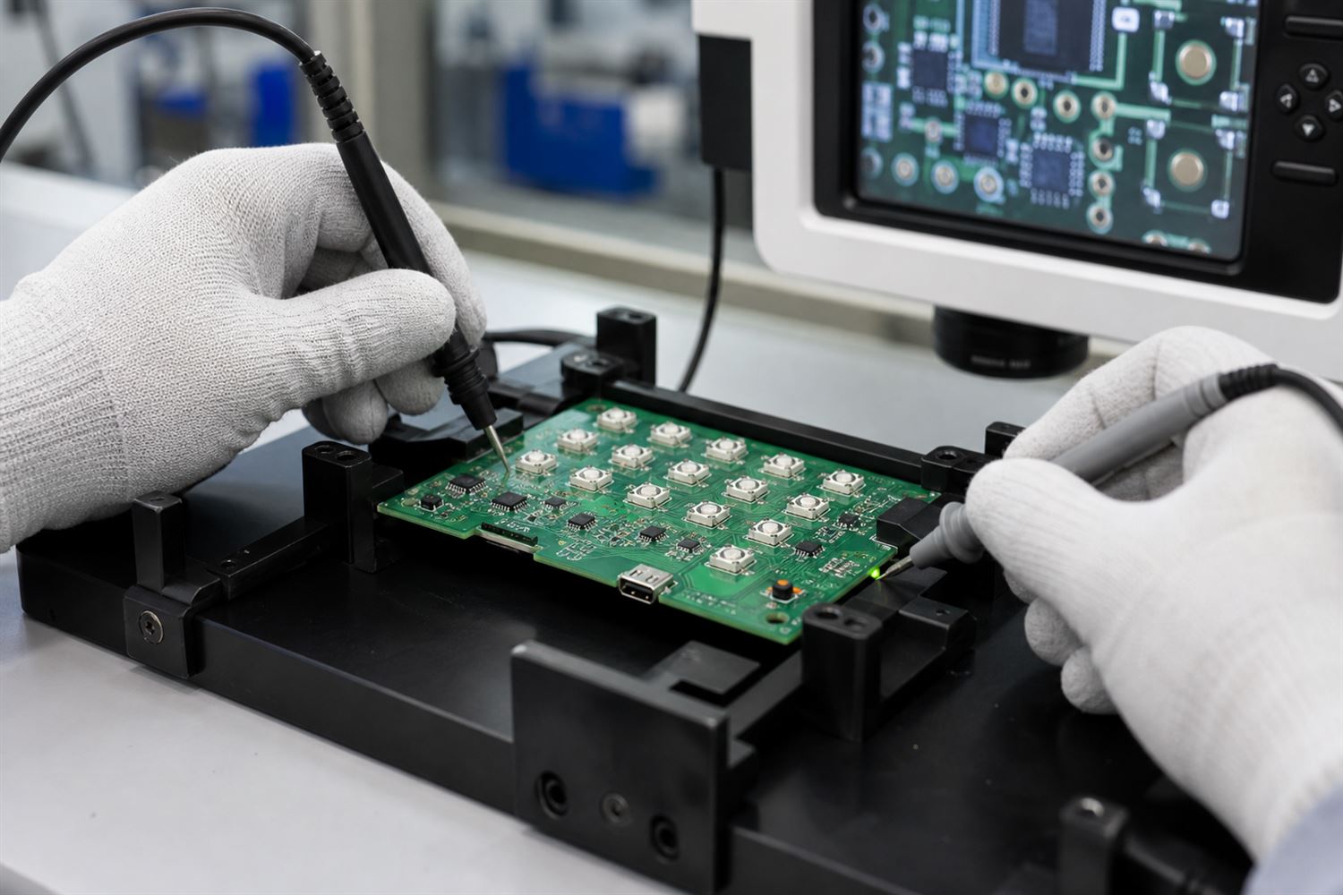
A GPS navigation PCB assembly combines a GPS or multi-constellation GNSS receiver with its antenna interface, processor, power supplies, memory and product communication circuits. It converts weak satellite signals into position and timing data that the host product can use for navigation, tracking or control.
Successful production depends on more than assembling the GNSS module. RF routing, power noise, board stackup, component placement, firmware and the functional test method must work together. EBest Circuit supports design review, PCB fabrication, component sourcing, SMT assembly, programming and customer-defined testing from prototype through repeat production.

Are you worried about your GPS navigation PCB assembly project?
- Could antenna placement, enclosure metal or an unreviewed RF substitution reduce receiver margin after assembly?
- Could power ripple, switching nodes or high-speed digital circuits interfere with acquisition or communication?
- Could incomplete programming and test requirements produce a prototype that cannot be released confidently for repeat builds?
With over 20 years of experience, EBest Circuit provides one-stop PCB and PCBA manufacturing support from design review and prototyping through repeat production.
- Protect receiver margin: We review the submitted stackup, RF feed, matching components, antenna interface and enclosure constraints before PCB release.
- Control the assembled configuration: We align the BOM, placement data, power requirements, firmware and assembly drawing so purchasing and production use the same revision.
- Build usable release evidence: We coordinate inspection, programming and customer-defined functional checks so prototype results can support the next production decision.
Ready to start your GPS navigation PCB assembly project? Send your PCB data, BOM, placement file, assembly drawing, module and antenna references, quantities and test requirements to sales@bestpcbs.com.
What Is a GPS Navigation PCB Assembly and How Does It Work?
A GPS navigation PCBA receives satellite signals, calculates or relays positioning data and passes that data to the host product. GPS is one GNSS constellation; many current receivers can also use Galileo, BeiDou or GLONASS. The approved module specification determines which constellations, interfaces and operating modes apply to the product.
The signal path normally runs from the GNSS antenna through an RF feed and matching network to the receiver. The receiver outputs navigation or timing data to an MCU or processor, which exchanges information with the display, cellular modem, CAN network, USB port or another host interface. Power-management circuits supply the receiver and, when used, an active antenna. Before assembly release, verify the module interface, antenna path and required output messages against the approved schematic and module documentation.
Where Are GPS Navigation PCB Assemblies Used?
GPS navigation PCB assemblies are used wherever a product must determine, report or act on location, speed or precise timing. The application changes the mechanical environment, interfaces, power states and acceptance tests that the manufacturer must plan.
- Automotive navigation and telematics: The PCBA may exchange data with vehicle networks, displays, cellular modules and sensors while operating near chargers, motors and other noise sources.
- Fleet and asset tracking: Low-power operation, cellular connectivity, enclosure size and antenna placement often control the design and test conditions.
- Marine and industrial positioning: Connector sealing, corrosion exposure, cable routing and external-antenna interfaces can become part of the manufacturing package.
- UAV and agricultural equipment: Vibration, power-converter noise, orientation and communication interfaces must be defined for the intended installation.
- Portable navigation products: Battery management, compact layout, display activity and enclosure interaction can affect both assembly and functional validation.
What Components Are Integrated on a GPS Navigation PCB?
The board combines the GNSS signal chain with processing, power and product interfaces. Each functional block creates a distinct placement, sourcing or verification task, so the design package should identify the exact component and the evidence required for release.
- GNSS receiver: Processes satellite signals and outputs position, velocity or timing data. Production must control the exact part number, package orientation, footprint and approved substitution boundary.
- RF path: Connects the antenna interface, filter, amplifier or matching network to the receiver. Review the feed geometry, reference plane, keepout, matching-component identity and connector condition.
- MCU or processor: Uses navigation data and controls product logic. Release its programming package, clocking, reset behavior and required interfaces with the assembly data.
- Power management: Supplies the receiver, processor and active antenna when used. Define the rail sequence, ripple-sensitive loads, regulator placement and measurement points.
- Memory and timing: Stores code or configuration and provides timing references. Control the exact device identity, oscillator layout, loading parts and programming data.
- Product interfaces: Connect UART, USB, CAN, Ethernet, cellular, Bluetooth or other product circuits. Identify connector orientation, protection parts, routing constraints and functional-test access.
How Do RF Layout and Antenna Integration Affect GPS Performance?
The RF feed must preserve the reference design from the antenna interface to the receiver. Loss, discontinuities, an interrupted return path or coupling from nearby electronics can reduce the usable signal margin before software processes the data.
The selected module and antenna documents remain the controlling sources. The u-blox GNSS antenna integration overview explains why the front-end RF path, interference filtering and antenna environment must be considered together. The actual stackup, antenna and enclosure still require project-specific review.
- Preserve the RF feed: Route the specified feed over its reference plane, control transitions and keep the matching network close to the location defined by the reference design.
- Protect the antenna zone: Apply the required copper, component and mechanical keepout around the embedded antenna or approved antenna interface.
- Control the enclosure boundary: Record nearby metal, cable routes, connector position and antenna orientation because these conditions can change the assembled RF environment.
- Restrict substitutions: Mark filters, matching parts, connectors and active-antenna components as do-not-substitute unless engineering approval includes the necessary retest.
- Provide inspection access: Define how RF connectors, shield joints and hidden receiver-module joints will be inspected without damaging the feed or antenna contact.
How Should Power Integrity and Digital Noise Be Managed?
The receiver needs a stable supply and physical separation from strong switching and digital noise sources. A board can communicate correctly on the bench yet lose receiver margin when a modem transmits, a display switches or a DC-DC converter enters a different operating mode.
- Define the power tree: Identify receiver and active-antenna rails, startup sequence, reset criteria, expected current states and the measurement points used during verification.
- Place converters deliberately: Keep switching nodes, inductors and high-current loops away from the RF feed, receiver input and timing components. Use the selected regulator and module guidance to set the boundary.
- Apply local decoupling: Place specified capacitors at the intended pins with short return paths so component placement matches the electrical design rather than a generic assembly convention.
- Test active noise states: Exercise the processor, display, cellular radio, charger, motor or other integrated loads that can create product-level interference.
- Record comparable conditions: Tie results to firmware, antenna, enclosure, supply source and operating mode so changes between builds can be evaluated.
How Should RF, Power and Digital Circuits Be Separated?
Partition the board by current path and noise sensitivity, then preserve continuous return paths between connected functions. Physical separation alone is insufficient if a noisy signal crosses the RF reference area or a plane opening forces return current around the receiver.
- Reserve the RF zone: Keep the receiver input, feed, matching network and antenna interface together and away from clocks, switching nodes and high-current connectors.
- Contain the power zone: Minimize the hot loop of each switching converter and route its input, switch node and output currents without crossing the RF area.
- Control digital routing: Route fast clocks, USB, memory buses and processor interfaces over continuous references and away from the antenna feed.
- Place timing parts carefully: Position the crystal or TCXO according to the component reference layout and avoid coupling from switching or high-speed nets.
- Plan shielding and test access: Locate shield fences, cans, programming pads and measurement points before routing is frozen so production can inspect and test the board without improvisation.
If a switching return crosses the RF reference area, supply noise can couple into the receiver input and cause slow or intermittent acquisition. Verify the final partition by reviewing current-return paths and repeating receiver tests while converters and high-speed interfaces operate in their defined active states.
What PCB Manufacturing Requirements Matter for GPS and GNSS Boards?
The PCB specification must preserve the RF reference, power return paths and package geometry required by the released design. Layer count or material should not be selected from the application name alone; the stackup, routing density, impedance needs and assembly packages determine the construction.
- Stackup and reference planes: Define layer order, dielectric thickness, copper weight and reference planes so controlled routes and return paths match the approved layout.
- Controlled features: State any impedance target, trace geometry, coupon or verification requirement that applies to the RF feed or other controlled nets.
- Material selection: Use the designer-specified FR-4 or RF material and its approved equivalent boundary. Do not replace material solely from a generic GPS label.
- Via and HDI structures: Specify through vias, blind or buried vias, via-in-pad treatment and fill requirements only where routing or package escape requires them.
- Surface and dimensional control: Define finish, solder mask, board outline, connector geometry and RF trace-etching requirements that affect assembly or interface fit.
- Fabrication evidence: Release the approved stackup, controlled-feature report and any inspection records required for prototype acceptance or repeat orders.
How Is a GPS Navigation PCB Assembly Manufactured?
The process converts one released PCB, BOM and assembly package into an inspected and programmed navigation board. Each operation must protect the GNSS module, RF parts, timing devices, connectors and shields identified by the design.

- Verify incoming materials: Match PCB revision, component part numbers, moisture requirements and approved substitutions to the purchase package. Quarantine discrepancies before they enter kitting, and retain the receiving record required by the order.
- Print and inspect solder paste: Use the released stencil and paste process for the actual pad geometry and thermal mass. SPI can detect deposit conditions covered by the plan before placement makes the defect harder to isolate.
- Place sensitive components: Load the approved program and verify pin-one, connector direction, GNSS module orientation, RF filters, matching parts and timing components. A first-article check should confirm these identities before the run continues.
- Reflow the assembly: Establish the profile for the actual board, solder and component limits. Monitor the defined profile evidence because an unrelated board’s profile does not prove suitable heating for the current module or shields.
- Inspect soldered joints: Apply AOI to visible conditions and X-ray where hidden joints create a documented risk. Record defects and disposition against the order’s acceptance criteria.
- Complete secondary operations: Install through-hole connectors, shields, cables or hardware using the approved drawing. Protect RF contacts and test points from residue or mechanical damage.
- Program and functionally test: Load the approved firmware, verify its identity and run the specified electrical and navigation checks. Save the result format required for prototype approval or traceability.
If the order invokes IPC requirements, state the revision and class. IPC distinguishes solder-process requirements in J-STD-001J from post-assembly acceptability in A-610J, as summarized in the IPC assembly standards release.
How Should GPS Navigation PCB Assemblies Be Tested?
Inspection verifies construction, while electrical and functional tests verify the customer-defined behavior. The test plan should separate visible solder evidence, hidden-joint evidence, power and interface checks, firmware control and GNSS operation.
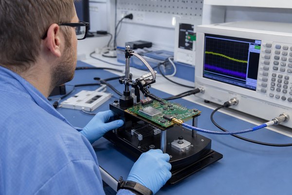
- Structural inspection: Use SPI, AOI, visual inspection and X-ray only for the conditions each method can observe. Define package targets, coverage and defect disposition instead of presenting one method as universal.
- Electrical checks: Measure specified rails, current states, shorts, opens and interfaces at named points with the fixture revision and pass limits recorded.
- Programming control: Verify firmware version, configuration, serialization and programming result before the navigation test begins.
- GNSS functional test: Check receiver communication, module status, antenna condition and required positioning outputs under the antenna, enclosure and operating conditions defined by the customer.
- Acceptance boundary: Assembly inspection does not certify final positioning accuracy. Product-level performance requires the customer’s defined environment, limits and validation method.
- Failure records: Preserve board identity, firmware, antenna state, power state and test setup so the team can distinguish an assembly defect from design, component, software or environmental causes.
How Is a Prototype Validated Before Mass Production?
The prototype stage must close design-transfer, sourcing, assembly and test risks before quantity increases. A board that acquires satellites once is not enough; the release package must show what was built, what changed and how later units will be judged.
| Release Area | Prototype Evidence | Volume Decision |
| Configuration | PCB, BOM, placement data, firmware, antenna and approved substitutions match | Freeze the as-built baseline and open exceptions |
| Assembly | First-article, solder, connector, shield and hidden-joint results as applicable | Approve the process or require corrective action |
| Power and interfaces | Startup, reset, rail, current and communication results under defined states | Set the repeatable electrical test limits |
| GNSS function | Customer-defined antenna, enclosure, operating mode and output results | Approve the functional method and result format |
| Supply continuity | Approved part numbers, lifecycle risks, alternates and material responsibility | Authorize purchasing for the planned quantity |
For pilot and repeat production, carry forward the approved BOM, firmware, assembly notes, test limits and exception record. Any change to the GNSS module, RF components, antenna, enclosure or power architecture should invalidate the affected evidence and trigger the relevant review or retest.
What Common Problems Cause GPS Navigation PCBA Failures?
Most failures can be narrowed by linking the symptom to the RF path, power state, assembled configuration or test environment. Diagnosis should reproduce the reported condition before changing parts or retuning the design.
- Weak or unstable reception: Inspect the antenna contact, RF connector, feed continuity, matching-part identity and enclosure changes. Compare the result with the approved antenna condition.
- Slow or intermittent acquisition: Measure supply ripple and startup states, confirm firmware identity and repeat the test while defined product circuits are active.
- No receiver communication: Check module orientation, solder joints, reset, clock, interface activity and programming configuration before replacing the receiver.
- Active antenna fault: Measure the defined bias supply and inspect the protection circuit, connector and cable path under the approved load condition.
- Enclosure-only failure: Compare bare-board and enclosure results with the same firmware and power state, then inspect nearby metal, cable routing, orientation and internal radio activity.
What Affects GPS Navigation PCB Assembly Cost and Lead Time?
The cost and schedule for GPS navigation PCB assembly depend on material availability, board complexity, package mix, inspection coverage, programming, fixtures, functional-test time and order quantity. A quote is comparable only when each supplier prices the same released scope.
- Component availability: Allocated navigation modules or buyer-restricted parts can determine the material schedule. Approved alternatives and consigned parts change both risk and commercial responsibility.
- PCB construction: Layer count, controlled impedance, specified RF material, HDI structures, finish and dimensional requirements affect fabrication cost and schedule.
- Assembly complexity: Fine-pitch packages, bottom-terminated parts, shields, RF connectors and mixed SMT/through-hole operations affect tooling, inspection and rework exposure.
- Test scope: Fixture design, firmware loading, electrical checks, RF connections and product-specific navigation tests should be quoted explicitly. A lower price that omits agreed evidence is not an equivalent offer.
- Prototype learning: Unresolved DFM questions, test-method gaps or unstable BOM revisions lengthen the path to volume release. Closing them in the prototype reduces avoidable changes later.
- Order profile: Prototype, pilot and repeat production use different quantities, setup effort and material commitments. Provide the current quantity and forecast instead of requesting one price for an undefined range.
What Files Are Needed for a GPS Navigation PCB Assembly Quote?
An accurate quote needs one released, internally consistent package that identifies what will be fabricated, purchased, assembled, programmed, inspected and tested. Missing or conflicting files force the supplier to make assumptions that later change price or delivery.
- PCB data: Gerber or approved intelligent data, drill files, board outline, stackup, material, copper, finish and controlled-feature notes.
- BOM: Complete manufacturer part numbers, quantities, approved alternatives, do-not-substitute items and any consigned material.
- Placement data: Reference designator, X/Y position, rotation, side and origin convention matching the released assembly drawing.
- Assembly drawing: Polarity, connector direction, shields, hardware, special soldering, antenna keepouts and workmanship notes.
- Module and antenna references: Relevant datasheets, layout guidance, matching details and approval boundaries for the selected configuration.
- Programming package: Firmware identity, programming method, security or serialization inputs and verification output.
- Test specification: Fixture interface, power states, measurement points, limits, navigation conditions, sampling or full-test requirement and result format.
- Commercial inputs: Prototype and production quantities, target schedule, delivery location, packaging, traceability and required quality records.
Why Choose EBest Circuit for GPS Navigation PCB Assembly?
EBest Circuit gives buyers one project path for PCB fabrication, component sourcing, SMT assembly, programming coordination and customer-defined testing. This reduces handoff gaps between board production, parts and assembly while keeping the approved design and evidence requirements visible.
- One-stop PCB and PCBA: Coordinate fabrication, sourcing, SMT, secondary assembly and project records through one manufacturing handoff.
- RF-focused manufacturability review: Check submitted stackup, controlled routes, receiver footprint, matching-part placement, shield and connector requirements before release.
- GNSS module assembly control: Tie exact module identity, orientation, moisture handling and approved substitutions to the released BOM and drawing.
- Programming and test coordination: Build the supplied firmware, fixture, limits and result format into the production package instead of treating testing as an undefined add-on.
- Prototype-to-volume continuity: Transfer the approved as-built configuration, exceptions and test evidence into pilot and repeat orders.
- Traceable project response: Return DFM questions, sourcing risks and missing evidence against the submitted files so the buyer can close specific release decisions.
FAQs About GPS Navigation PCB Assembly
Q1: Does every GPS navigation board require a controlled-impedance RF trace?
A1: Follow the selected module and antenna reference design. The required feed structure, impedance target and layout depend on the chosen configuration. Specify the approved feed geometry, stackup reference, matching locations and acceptance method in the released PCB data rather than assuming every module uses the same structure.
Q2: Can AOI confirm GPS or GNSS reception?
A2: No, AOI verifies visible assembly conditions. Navigation performance needs a separate customer-approved functional method with the defined antenna, firmware, power state, enclosure and signal environment. Keep the AOI record and functional result separate so each one proves only what it actually checks.
Q3: Can FR-4 be used for a GPS navigation PCB?
A3: Use the material specified by the released stackup and RF design. Many navigation boards may use FR-4, while a design with different loss, frequency or routing constraints may specify another material. Confirm the impedance, geometry and supplier-approved material boundary rather than selecting by product name alone.
Q4: Can EBest source the GPS or GNSS module?
A4: Component sourcing can be included in the project scope. Supply the exact manufacturer part number, approved alternatives and any date-code or traceability requirements for review. Parts that affect RF, timing, firmware or regulatory evidence should remain do-not-substitute unless the approval process says otherwise.
Q5: Can a GPS navigation PCB include cellular, Bluetooth or CAN interfaces?
A5: Yes, when the product architecture and layout support them. Define each interface, its power state, routing constraints and simultaneous operating modes. Wireless transmitters and high-speed circuits should be active during the relevant interference and functional checks.
Q6: Can a module substitution be approved from the footprint alone?
A6: No, mechanical compatibility does not prove functional equivalence. Check electrical, RF, firmware, regulatory, lifecycle and test implications before approving a replacement. Record the approved alternative and any required retest against the affected board and firmware revision.
Q7: Where should the GNSS module be placed on the PCB?
A7: Follow the selected module reference layout and the board’s RF partition. Keep the receiver input and antenna feed away from strong switching and digital noise sources, preserve its reference plane and leave the required antenna or connector boundary intact.
Q8: What makes a GPS navigation PCBA quote change?
A8: Scope changes alter material, setup and test effort. Common causes include BOM revisions, unavailable parts, added inspection, new fixtures, firmware changes, quantity changes and missing acceptance criteria. Compare quotations only after these assumptions and their validity periods are stated in writing.
Q9: Does every navigation PCBA need X-ray inspection?
A9: No, X-ray should follow package and hidden-joint risk. Use it when the GNSS module, processor or another bottom-terminated package requires internal evidence under the inspection plan. Visible joints still need the appropriate visual or optical checks.
Q10: What should buyers send first for a manufacturability review?
A10: Send the complete released PCB and assembly package. Include the BOM, placement data, drawings, module and antenna references, quantities, programming method and test requirements. Consistent revisions let the supplier identify open decisions without rebuilding design intent from separate emails.
Conclusion
A production-ready navigation PCBA connects receiver architecture, RF integration, power integrity, PCB construction, assembly and functional testing under one approved configuration. That connection lets engineering diagnose real product risks and gives purchasing a comparable basis for scope, price, lead time and repeat-production evidence.
EBest Circuit can review your project from PCB fabrication and component sourcing through prototype assembly, programming coordination and repeat production. Send the Gerber or approved intelligent PCB data, BOM, placement file, assembly drawing, module and antenna references, quantities and test specification to sales@bestpcbs.com for a project-specific DFM review and quotation.