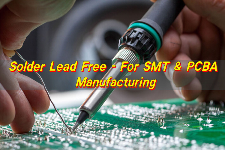
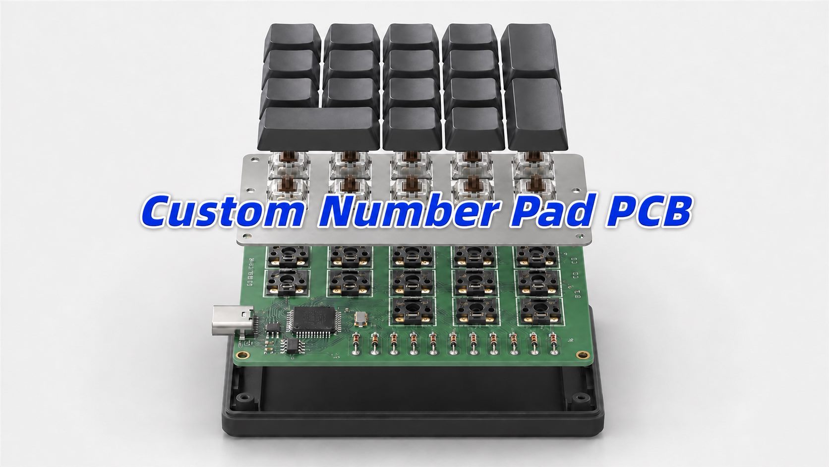
A custom number pad PCB is a purpose-built circuit board that connects a numeric key layout, switch matrix, controller and wired or wireless interface in one production-ready assembly. A reliable design starts with the user interface and enclosure, then translates that geometry into switch footprints, row-and-column scanning, diode orientation, connector protection, fabrication data and a repeatable test plan.
That sequence matters. A numpad can work on a development bench and still fail in production because a hot-swap socket collides with the enclosure, a diode direction does not match the firmware, a USB-C connector lacks the required configuration resistors, or the assembly supplier receives incomplete files. This guide shows engineers, buyers and product teams how to move from a custom layout to a PCB and PCBA package that a manufacturer can quote, build and inspect without guessing.
What Is a Custom Number Pad PCB?
A custom number pad PCB is the electrical and mechanical platform for a numeric keypad made for a specific product, layout or workflow. Unlike a replacement PCB for an existing retail numpad, a custom board can change the key count, key positions, macro functions, switch technology, interface, mounting pattern, controller and enclosure.
The term can describe several products:
- A mechanical numpad with MX-style or low-profile switches.
- A programmable macropad that includes numbers, shortcuts, a rotary encoder or display.
- An industrial data-entry panel with tactile switches, metal domes or a membrane interface.
- A compact control PCB integrated into a larger instrument, terminal or machine.
- A wired USB device or a battery-powered wireless input module.
The PCB is only one part of the input system. It must fit the plate and enclosure, accept the selected switches, scan every key reliably, communicate with the host and survive assembly and use. For a broader overview of full-size and compact keyboard projects, see the Best Technology guide to custom keyboard PCB development.
Which Numpad Architecture Fits the Product?
The right architecture depends on whether the number pad is a finished USB device, a keypad module inside another product or a low-power wireless controller. Decide this before assigning controller pins or routing the board.
| Architecture | Best fit | Key design decisions | Production concern |
|---|---|---|---|
| USB numpad | Desktop data entry, POS accessories, programmable controls | USB-capable MCU, Type-C or legacy connector, ESD and firmware | Connector strength, USB compliance and functional testing |
| Matrix keypad module | Industrial equipment, instruments and embedded products | Row/column connector, voltage levels, cable length and host scanning | Connector pinout, noise immunity and system-level test access |
| Wireless numpad | Portable or cable-free products | Radio module, antenna clearance, battery management and sleep current | RF layout, enclosure material, certification scope and power test |
| Industrial front-panel keypad | Sealed controls and repetitive data entry | Metal dome, membrane or tactile switch interface; ESD and ingress strategy | Overlay stack-up, actuation consistency and environmental validation |
A stand-alone USB numpad usually needs the most integration on the PCB. A passive matrix keypad may need no onboard MCU, but the row/column interface, cable pinout and host-side scanning must be defined. Wireless designs add antenna, power and regulatory constraints that should not be treated as a simple variation of the wired board.
How Should the Key Matrix and Diodes Be Designed?
A numpad matrix arranges switches at row-and-column intersections so the controller can scan many keys with fewer I/O pins. A 5-by-4 matrix, for example, can address up to 20 switch positions with nine matrix signals, although the actual layout may leave some intersections unused.
During scanning, firmware drives or reads one side of the matrix and checks the other side to identify a closed switch. The official QMK matrix explanation illustrates why multiple simultaneous keypresses can create unintended current paths. A diode in series with each switch makes current directional and helps prevent ghost keys.
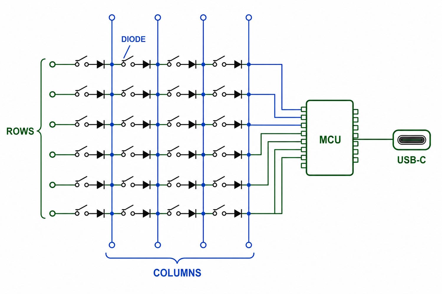
Use this matrix checklist before layout:
- List every key, encoder push switch and auxiliary button in a matrix table.
- Choose row and column counts that fit the available MCU pins and expected expansion.
- Assign one reference designator to every switch and diode.
- Use a single diode orientation across the board unless the design has a documented exception.
- Set the firmware diode direction to match the schematic. QMK exposes this through its matrix configuration options.
- Reserve accessible test points for rows, columns, power, ground and reset.
- Review simultaneous-key requirements instead of testing only one key at a time.
A small numpad may appear to work without per-key diodes when users press one key at a time. That does not prove the matrix is safe from ghosting. Diodes are especially important when the product supports shortcuts, macros, gaming inputs or any action that combines multiple keys.
How Do You Choose Switches, Hot-Swap Sockets and Key Spacing?
Choose the input technology before creating footprints because the switch, socket, plate and enclosure form one mechanical stack. A footprint that is electrically correct can still be unusable if the switch orientation, stabilizer cutout or component height is wrong.
| Input option | Advantages | Trade-offs | Layout checks |
|---|---|---|---|
| Soldered mechanical switch | Simple BOM and strong retention | Switch replacement requires soldering | Pin pattern, center post, plate cutout and stabilizers |
| Hot-swap socket | Replaceable switches and easier product customization | More underside area and tighter enclosure constraints | Socket orientation, copper clearance, solder access and bottom-case height |
| Low-profile switch | Thinner product | Different footprint, plate and keycap ecosystem | Exact manufacturer drawing and total stack height |
| Tactile switch or metal dome | Compact industrial interface | Different feel and front-panel construction | Contact geometry, actuation force, overlay and venting strategy |
Many mechanical layouts use a 19.05 mm key pitch, but that value is not a universal rule. Start from the chosen switch and keycap drawings, then define the plate, PCB and enclosure from one controlled coordinate system. Pay special attention to double-width Enter or Plus keys, stabilizer locations, rotary encoders, displays and USB connector openings.
What Should a USB-C Numpad Circuit Include?
A USB-C numpad circuit needs more than the connector footprint: it must define device orientation detection, power protection, data routing and mechanical retention. For a basic USB 2.0 device using a Type-C receptacle, both CC pins normally require their own pull-down resistor to identify the board as a sink/device. Confirm the resistor value and implementation against the current USB Type-C specification and the selected connector or controller documentation.
The schematic and layout review should cover:
- CC1 and CC2 configuration for a device-only port.
- VBUS protection appropriate to the product risk and power path.
- ESD protection placed close to the connector.
- D+ and D− routing as a short, coupled pair with a continuous return path.
- Decoupling capacitors located close to MCU power pins.
- Connector shell grounding and mounting tabs based on the connector datasheet.
- Accessible reset and programming pads.
- Cable insertion clearance and enclosure wall thickness.
Do not copy a Type-C connector symbol or footprint without checking its pin mapping and mechanical drawing. A footprint mismatch can produce a board that looks correct in CAD but cannot be assembled or connected reliably. The BestPCBs article on USB port pin configuration provides additional connector context.
How Should the PCB Match the Plate and Enclosure?
The PCB, switch plate and enclosure should be designed from a shared mechanical datum and verified together in 3D. Board outline, mounting holes, connector openings and key centers must use controlled dimensions rather than visual alignment.
Review the following interfaces:
- Key centers: Export coordinates from the approved layout and lock them before detailed routing.
- Mounting holes: Define finished hole size, keepout, fastener head diameter and any plated or non-plated requirement.
- Board edge: Maintain clearance between copper/components and routed edges based on the fabricator’s rules.
- Connector position: Check insertion path, cable overmold and strain on the solder joints.
- Hot-swap sockets: Verify bottom-case clearance and prevent ribs or batteries from touching sockets.
- Component height: Place the tallest parts in permitted zones and include tolerance, not only nominal dimensions.
- ESD path: Consider where a user can touch exposed metal, a rotary encoder shaft or connector shell.
A STEP model or enclosure assembly review is useful, but it does not replace a dimensioned drawing. Include critical dimensions and tolerances in the controlled design package so the PCB, plate and enclosure suppliers work from the same revision.
What Files Are Required for Fabrication and Assembly?
A reliable quotation and build require a complete, revision-controlled fabrication and assembly package. Gerbers alone may be enough for a bare board quote, but they are not enough for turnkey PCBA.
| File or document | Purpose | Numpad-specific checks |
|---|---|---|
| Gerber or ODB++ fabrication data | Defines copper, solder mask, silkscreen, paste and board outline | Switch pads, socket paste openings, USB tabs and outline are on correct layers |
| Excellon drill files | Defines plated and non-plated holes | Switch posts, stabilizers and mounting holes are classified correctly |
| Fabrication drawing/readme | States stack-up, thickness, finish, impedance if required and special notes | Board thickness matches switches, sockets, plate and enclosure |
| BOM | Lists manufacturer part numbers, quantities and approved alternates | Connector, MCU, diode, ESD device and socket variants are unambiguous |
| Pick-and-place/centroid file | Defines component coordinates, side and rotation | Diode polarity and hot-swap socket rotation are verified against the drawing |
| Assembly drawing | Shows reference designators, polarity, do-not-fit parts and notes | Key-layout options and variant components are clearly separated |
| Test specification | Defines electrical and functional acceptance | Every key, multi-key condition, USB interface, LEDs, encoder and current mode is covered |
| Firmware/programming package | Defines image, method, version and verification | Keymap, diode direction, bootloader and product identifier match the PCB revision |
KiCad’s official documentation describes the generation of Gerber and drill outputs. Before release, open the exported manufacturing data in an independent viewer. Do not rely only on the native CAD display. BestPCBs also provides practical PCB design tools for trace-width and via-current checks during engineering review.
For a broader supplier-ready package, use the custom PCB assembly services checklist to review BOM, placement data, sourcing and test requirements.
Which DFM Checks Prevent Prototype Re-Spins?
The most valuable DFM review finds electrical, assembly and mechanical errors before the first panel is released. For a custom numpad PCB, the review should go beyond trace width and spacing.
- Confirm switch, socket, stabilizer, connector and encoder footprints against current datasheets.
- Run schematic-to-layout checks and verify every row, column and diode reference.
- Check diode and LED polarity in the schematic, silkscreen, BOM and placement file.
- Inspect solder mask and paste apertures for hot-swap sockets and connector mounting tabs.
- Check component-to-edge, copper-to-edge and tool clearance around routed features.
- Separate non-plated mechanical holes from plated electrical holes.
- Review USB D+/D− routing, return path, ESD placement and connector shell strategy.
- Verify annular rings, thermal reliefs and solderability for hand-soldered or through-hole parts.
- Add readable revision marking and polarity/orientation identifiers.
- Check panelization, breakaway features and component clearance near panel rails.
- Compare the final PCB model with the plate and enclosure assembly.
- Review test-point access after the board is installed in its fixture or enclosure.
Variant control is another common failure point. If one PCB supports several key layouts or optional displays, document fitted and non-fitted parts by assembly variant. Do not leave the assembler to infer the product version from the order name.
How Is a Custom Number Pad PCB Manufactured and Assembled?
Production moves from engineering review to bare-board fabrication, component assembly, inspection and product-specific functional testing. The exact flow depends on the stack-up, component mix, quantity and acceptance plan.
- Engineering review: The supplier checks file completeness, fabrication constraints, BOM availability and assembly risks.
- Panel and tooling preparation: The board is arranged for fabrication and, when required, automated assembly.
- Bare PCB fabrication: Imaging, etching, drilling, plating, solder mask, surface finish, profiling and electrical test create the finished board.
- Component preparation: Parts are sourced, verified and assigned to the correct BOM revision and alternates list.
- SMT assembly: Solder paste printing, placement and reflow attach the MCU, diodes, ESD devices, LEDs and other surface-mount parts.
- Through-hole/manual assembly: Connectors, switches or special components are installed when they are not part of the SMT process.
- Inspection: Visual inspection and AOI can verify placement and solder joints; X-ray may be appropriate for hidden-joint packages.
- Programming and functional test: When included in the agreed scope, the board is programmed and tested against the approved procedure.
- Final inspection and packing: The supplier confirms labeling, quantity, protection and shipment requirements.
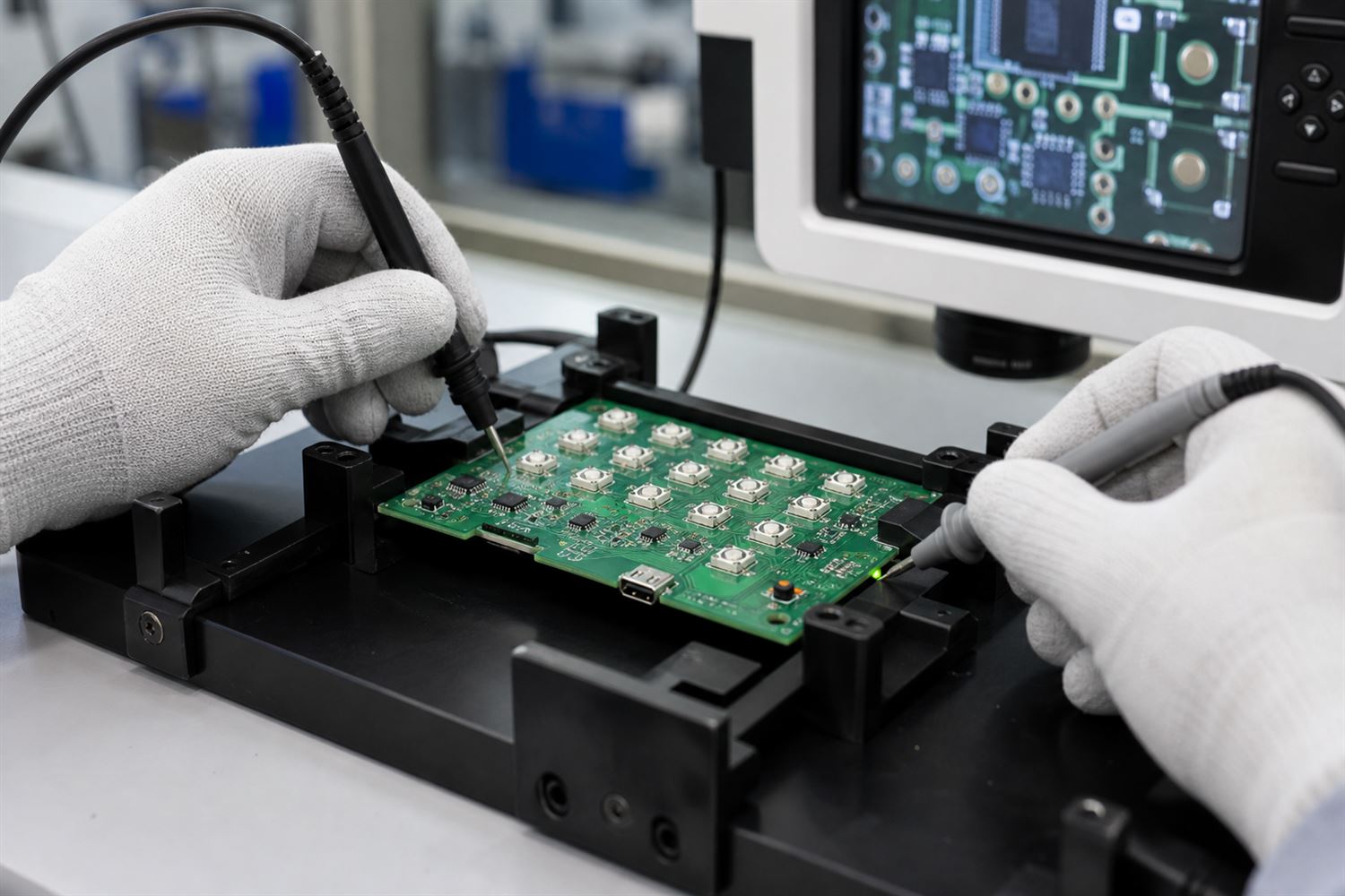
Best Technology supports PCB design, prototyping, component sourcing, PCB assembly and small-volume production. Available inspection and test methods documented in the company’s source materials include AOI, X-ray inspection, flying-probe/electrical testing and functional testing. The correct combination should be defined for the actual board rather than copied from a generic quality plan. Learn more about the company’s PCB manufacturing process and PCB assembly capabilities.
How Should the Finished Numpad PCB Be Tested?
A finished numpad needs both board-level checks and a functional test that exercises every input and interface. A bare-board electrical test cannot verify firmware, switch behavior, LEDs, USB enumeration or enclosure interactions.
A practical acceptance plan may include:
- Power-rail resistance and controlled first power-up.
- Current consumption in active, idle and sleep modes when applicable.
- USB enumeration and communication using the approved cable and host conditions.
- Continuity or scan verification for every row and column.
- Single-key test for every switch position.
- Multi-key combinations that could expose ghosting or firmware mapping errors.
- Rotary encoder direction, push switch, display and indicator LED tests.
- Reset, bootloader and programming-pad access.
- Mechanical fit with the production plate, keycaps, enclosure and cable.
- Stress, ESD, life-cycle or environmental testing defined by the product’s risk and market.
A test fixture can speed up repeatable production checks, but the fixture requirement should be defined early. Add test pads before routing is complete and provide the supplier with the test sequence, pass/fail limits, firmware revision and expected output.
What Drives Prototype and Production Cost?
Cost is driven by board complexity, component choices, assembly operations, testing and order quantity—not by key count alone. A physically small numpad can still be expensive if it uses a high-cost controller, several assembly variants or a complex test fixture.
| Cost driver | Why it matters | Cost-control action |
|---|---|---|
| Board size and layer count | Affects material use, panel utilization and process complexity | Route compactly without compromising switch geometry or test access |
| Surface finish and specifications | Special finishes and tight requirements add process cost | Specify what the application needs; avoid unsupported blanket requirements |
| MCU and connector selection | Availability, package and sourcing risk affect price and schedule | Use complete MPNs and approve alternates through engineering review |
| Hot-swap sockets, LEDs and displays | Add components, placements and inspection points | Offer features only when the product requirement supports their value |
| SMT and through-hole mix | May require multiple assembly operations | Design for the intended assembly process from the first prototype |
| Programming and functional test | Requires files, labor, fixtures and failure handling | Create a short, deterministic test with clear pass/fail criteria |
| Variants and quantity | Frequent changeovers reduce production efficiency | Standardize the base PCB and control variants through BOM and firmware |
For a useful comparison, request quotes against the same revision, BOM assumptions, test scope and packing requirements. A lower line-item assembly price may not be lower total cost if it excludes component verification, programming, fixtures or rework responsibility.
How Do You Select a PCB/PCBA Supplier?
Select a supplier by its ability to review the complete product package and control revisions, sourcing, assembly and testing—not only by the bare-board price. The RFQ should make technical scope comparable across suppliers.
Ask these questions:
- Will the supplier review the native design or exported fabrication package for DFM and DFA risks?
- Can it build both the prototype and the intended production quantity without changing the approved process unexpectedly?
- How are BOM substitutions proposed, approved and recorded?
- Which inspection methods apply to the actual component package and defect risks?
- Can the supplier follow a customer-provided programming and functional test procedure?
- How are PCB, BOM, firmware and test revisions linked to the manufacturing order?
- Who owns fixtures, programming adapters and product-specific test assets?
- What information is required before the quotation becomes firm?
- How are nonconformities documented, contained and corrected?
- Can the supplier provide one point of coordination for PCB fabrication, component sourcing and assembly if that is required?
Send the same controlled file package to every candidate. If one supplier identifies a real footprint, sourcing or test problem, treat that engineering feedback as part of the comparison rather than focusing only on unit price.
Frequently Asked Questions
What is a custom number pad PCB?
A custom number pad PCB is a circuit board designed for a specific numeric keypad layout, switch type, controller, interface and enclosure. It may operate as a complete USB or wireless device or as a keypad module inside another product.
How does a numpad key matrix work?
A numpad matrix connects switches at row-and-column intersections. The controller scans the rows and columns to identify which intersection has closed, reducing the number of I/O pins required.
Does every numpad switch need a diode?
Use one diode per key when the design must prevent ghosting during multiple simultaneous keypresses. Keep diode orientation consistent and match the firmware’s row-to-column or column-to-row setting.
Can a custom numpad PCB use USB-C?
Yes. A USB-C numpad can use USB 2.0 data, but the schematic must correctly implement CC pins, power protection, ESD control, D+/D− routing and connector mechanics.
What files are needed to manufacture a numpad PCB?
For a bare PCB, provide Gerber or ODB++ data, drill files and fabrication notes. For PCBA, also provide a BOM, pick-and-place file, assembly drawing, approved alternates, firmware package and test specification as applicable.
Should a numpad use hot-swap sockets or soldered switches?
Hot-swap sockets support switch replacement and customization but consume underside space and require careful footprint orientation. Soldered switches simplify the BOM and provide strong retention but are harder to replace.
Can QMK be used for a custom number pad?
Yes, when the selected microcontroller and board configuration are supported. The matrix dimensions, pin assignments, diode direction, keymap and optional features must match the hardware.
How do you prevent ghosting in a keypad matrix?
Place a correctly oriented diode in series with each key, configure firmware to the same direction and test realistic multi-key combinations. A single-key test cannot prove that ghosting is controlled.
What should be tested before mass production?
Test power, USB or host communication, every key, multi-key combinations, LEDs, encoders, reset/programming access and mechanical fit. Add product-specific ESD, life-cycle or environmental tests according to risk.
What affects custom numpad PCB cost?
Key cost drivers include board size and layers, controller and connector choice, switch/socket type, LEDs or displays, SMT and through-hole operations, programming, functional testing, variants and quantity.
How do you choose a numpad PCB manufacturer?
Compare DFM support, revision control, sourcing process, assembly capability, inspection, functional testing and prototype-to-production continuity. Quote every supplier with the same controlled files and acceptance scope.
Can a supplier assemble the PCB and program the controller?
Some PCBA suppliers can do both, but programming is not automatic. Define the firmware image, programming method, security requirements, version verification, fixture ownership and functional test before ordering.
From Prototype to Production
The fastest path to a dependable custom number pad PCB is a controlled release package: approved layout, verified matrix, checked USB interface, complete manufacturing data and a test procedure tied to the same revision. That package gives engineering, procurement and the PCB/PCBA supplier one source of truth.
Best Technology can support PCB design, PCB prototyping, component sourcing and PCB assembly for custom input-device projects. To request an engineering review or quotation, contact Best Technology and include the board files, BOM, target quantity, enclosure constraints and test expectations. The team can then identify missing information and confirm a project-specific manufacturing scope without relying on assumptions.