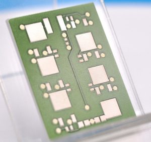
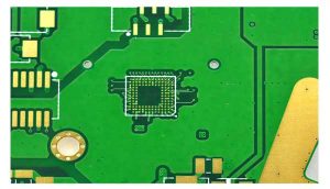
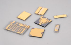
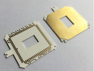
Copper edge relief is a local reduction of copper near a pad perimeter on a direct-bonded copper (DBC) ceramic substrate. It can reduce stress near the copper edge during temperature cycling, but it is not a universal pattern or a guaranteed life extension. Compare a relieved layout with an unrelieved control, and check that the remaining copper still meets the electrical, thermal and assembly requirements.
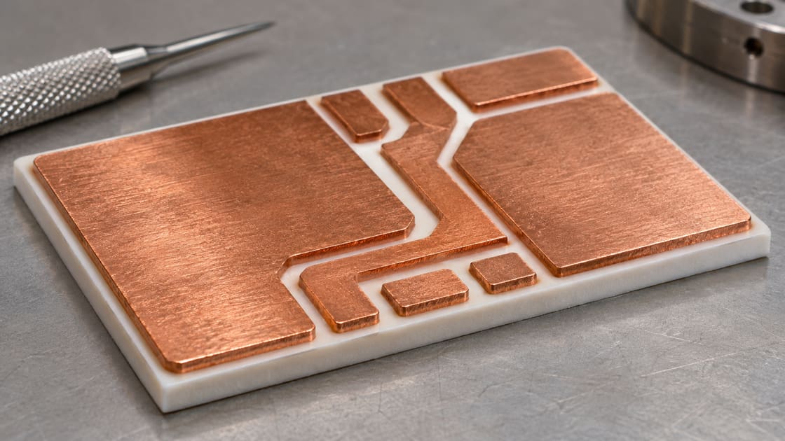
Why cracks can start beside a copper pad
Copper and ceramic expand by different amounts when the temperature changes. Because they are bonded, each constrains the other, and stress can concentrate near a copper island’s perimeter. Rogers’ reliability discussion describes this mechanism in metallized ceramic substrates. It does not imply that every crack in that region has the same cause.
What edge relief changes
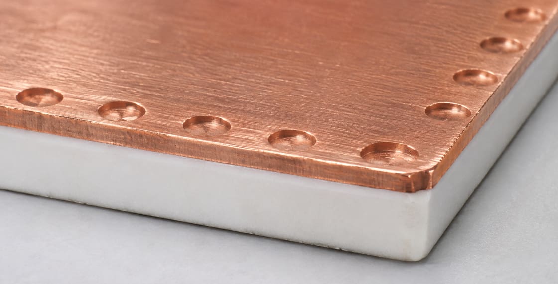
A relief feature changes the copper section near an edge rather than changing the whole ceramic. One supplier implementation uses shallow copper dimples near pad edges. A supplier drawing should distinguish a recess in copper from a through-hole or a gap in the electrical pattern. For the underlying construction, see this overview of DBC ceramic substrates.
Which dimensions to include in the comparison
Record the full stack and the remaining copper where the relief is deepest. There is no universal dimple size or pitch suitable for every design.
| Field | Unit or basis | What to compare |
| Ceramic and thickness | Grade and mm | Same grade and thickness in the control and relief variant |
| Front and back copper | Finished thickness in mm | Both faces, not just the component side |
| Relief geometry | Width, spacing and distance from edge in mm | Features aligned to a documented datum |
| Residual copper | Minimum remaining thickness in mm | Section where current or spreading heat could be constrained |
| Temperature cycle | Low and high setpoints in °C; dwell and ramp | Same defined test profile for both variants |
| Failure criterion | Agreed inspection and functional limits | Same initial baseline and end criterion |
Relief vs copper balance vs changing the substrate
Start with the change that addresses the observed mechanism and is feasible for the application.
| Option | What it changes | What else to verify |
| Local copper edge relief | Copper section near selected perimeter zones | Remaining current path, inspectability and usable attach area |
| Copper distribution adjustment | Front-to-back pattern balance | Flatness, insulation spacing and whether the change alters other copper features |
| Different ceramic or bonding system | Material and interface behavior | Thermal performance, electrical isolation, supply and qualification |
| Unrelieved control | Retains the original edge and stack | Baseline against which proposed improvements are measured |
How to keep relief away from the current path
Check the narrowest conducting section, not just the nominal copper thickness in the order. Imagine a power terminal feeding a copper island along one edge. Relief along the opposite unused perimeter may have a different impact from relief under the terminal feed. If the pattern intrudes into a high-current neck, check the actual remaining section before approving it. In a purely illustrative stack with 0.30 mm finished copper and a 0.08 mm recess, the nominal copper remaining at the recess bottom is 0.22 mm. Those figures are not a recommendation or a current rating; check the toleranced section and the actual current path.
How to protect the die-attach area
Keep the proposed relief separate from the die footprint and required attach land unless the assembly has been designed and qualified for that geometry. Check where heat enters the substrate and where the copper spreads it. A mechanically helpful detail can still be unacceptable if it reduces the attachment area or changes the thermal path.
Why the back copper belongs in the drawing
Record both faces because the stress depends on the whole cross-section and pattern. A nearly solid back face and a heavily segmented front face are not equivalent to two matching patterns. Review the copper-free perimeter, alignment and flatness along with the relief itself.
How to make a meaningful test coupon
Build a control and a relief variant that differ only in the intended feature where practical. Use the same ceramic, copper construction, layout at the area of interest and relevant assembly conditions. If a supplier also changes the ceramic, the test compares two systems rather than isolating the effect of relief.
Which temperature-cycle details belong in the report
Record setpoints, dwell, ramp or transfer conditions, fixture configuration and inspection intervals. Two tests with the same cycle count can impose different stress histories. An accelerated result ranks specimens under those conditions; it does not directly predict service life.
How to tell whether an indication matters
Locate the indication relative to the die, contact pads, copper edge and insulation boundary. A scanning acoustic microscopy image can help locate internal indications on a suitable sample, but interpret it with the baseline and geometry. When the heat path is at issue, correlate the inspection result with a relevant thermal measurement.
What to review if the modified pad still cracks
Compare the failure sites across control and variant. If cracks shift rather than disappear, review ceramic edges, copper pattern balance and local geometry. If both variants fail at a similar location, check specimen preparation, attachment conditions and the proposed failure mechanism before adding more relief.
What to send for a substrate review
Provide both copper layouts, the substrate grade, nominal and minimum dimensions, attach locations, operating temperature profile and qualification criteria. For manufacturing review, send the package to Best Technology at sales@bestpcbs.com and identify the required evidence rather than requesting a generic dimple pattern.
FAQ
Does every DBC substrate need dimples?
No. The decision depends on the construction and the failure mechanism in the intended use. A supplier may use a different geometry or material strategy. Compare against a control under the same conditions rather than treating the feature as mandatory.
Are dimples the same as copper vias?
No. In this context a dimple refers to a localized recess in the copper intended to change the edge geometry. It is not a plated interconnect. Confirm the depth and residual thickness in a section drawing rather than inferring the structure from a top-view photo.
Can thermal cycling tell me how long the product will last?
Not on its own. The test compares specimens under a defined temperature history. Service conditions also involve the operating profile and the assembled module. A lifetime claim needs a justified relationship between those conditions and the observed mechanism, supported by suitable validation.
Can I transfer the same geometry from alumina DBC to another ceramic?
Do not assume it transfers unchanged. Ceramic properties, copper thickness, joining system and geometry all affect stress. Treat a substrate change as a new design input and confirm the geometry and qualification plan for that particular construction. Keep the original test result tied to its original stack.
Is a visible ceramic crack always caused by copper expansion?
No. The position can suggest a mechanism, but handling, machining, assembly and pre-existing defects also need consideration. Use baseline inspection, test history and failure analysis to separate a cycling-related change from an indication that was already present. Compare equivalent locations across samples.
Will thicker copper always be worse?
No universal rule covers every geometry and stack. Extra copper can support current and heat spreading while increasing stress in some constructions. Compare the full system under the agreed electrical, thermal and mechanical conditions rather than ranking it by one thickness.
Should I compare copper relief on both faces at the same time?
If you want to isolate the effect of relief on one face, keep the other face unchanged in the control. If both faces must change in production, a separate matched test can evaluate the combined configuration. Label the two comparisons separately in the report.
Can I approve the design using an acoustic image alone?
Use the agreed acceptance criteria. An image can locate an indication but may not quantify its electrical or thermal consequence. Keep the baseline images and correlate them with relevant measurements if the indication lies near a critical function. Record the inspection resolution and interpretation limits.