Are you struggling with image sensor PCB signal noise, unstable MIPI transmission, or repeated assembly defects? Power supply ripple, impedance variations, and poor solder connections can cause image artifacts, communication errors, and expensive PCB revisions. Even a correctly designed CMOS image sensor may fail to perform as expected when the board’s electrical and manufacturing requirements are not properly controlled.
EBest Circuit provides custom image sensor PCB manufacturing, HDI fabrication, component sourcing, and SMT assembly for industrial cameras, machine vision systems, medical imaging equipment, and security devices. We help customers reduce PCB-related signal noise risks, prevent manufacturing defects, and maintain consistent production quality. Learn which design parameters matter, how to address common noise problems, and what manufacturing controls support reliable image sensor PCBs.

What Are the Critical Design Parameters for an Image Sensor PCB?
The most important image sensor PCB parameters are layer count, board thickness, trace geometry, controlled impedance, via structure, and sensor mounting accuracy. These specifications must match the sensor package, interface speed, routing density, and mechanical requirements.
For compact CMOS camera boards, fine-pitch routing and positioning accuracy are often critical. High-speed image acquisition PCBs may also require additional reference planes and controlled-impedance routing.
| Parameter | Design Reference / Manufacturing Capability | Application Requirement |
|---|---|---|
| PCB layers | 4, 6, or 8 commonly used; standard FR-4 capability of 1–10 layers | Select according to routing density and signal requirements |
| Board thickness | Common options: 0.8, 1.0, and 1.6 mm | Match sensor mounting and enclosure clearance |
| Copper thickness | 0.5–1 oz commonly considered for signal layers | Balance fine-line routing and current requirements |
| Trace width/spacing | Standard 4/4 mil (0.10/0.10 mm); special 3/3 mil (0.075/0.075 mm) | Depends on copper thickness and fabrication process |
| Laser microvia | 0.10 mm minimum process reference | HDI sensor fanout and dense interconnections |
| Finished mechanical hole | Standard 0.20 mm; special 0.15 mm | Interlayer connections and mounting requirements |
| MIPI D-PHY impedance | Common device-specific targets include 95 Ω or 100 Ω differential | Follow transmitter and receiver requirements |
| Surface finish | ENIG, ENEPIG, or OSP | Match the sensor package and soldering process |
| Mechanical accuracy | Critical dimensions and tolerances defined by the approved drawing | Ensure correct sensor positioning and mechanical fit |
For a fine-pitch image sensor package, pad dimensions, solder-mask openings, and via locations must also match the component manufacturer’s recommended footprint. Incorrect geometry can cause soldering problems even when the bare PCB passes electrical testing.
The complete manufacturing requirements should be specified in the fabrication drawing, including controlled-impedance nets, critical dimensions, and applicable acceptance tolerances. Special fine-line and microvia combinations require confirmation against the actual PCB construction.
How to Choose the Right Materials and Stackup for an Image Sensor PCB?
FR-4 is suitable for many standard image sensor PCBs, while high-Tg FR-4 and specialized laminates are used when thermal or signal-loss requirements demand them. A 4-layer PCB can support many compact CMOS sensor designs, while 6-layer and 8-layer constructions provide more routing space for dense or high-speed applications.
Material selection depends on the operating environment and electrical requirements:
- Standard FR-4: Suitable for many security camera boards, industrial CMOS image sensors, and conventional imaging circuits.
- High-Tg FR-4: Provides greater thermal margin for demanding operating or assembly conditions.
- Low-Loss Laminates: Considered when the required signal-channel performance cannot be achieved with the proposed FR-4 construction.
- Flexible Polyimide: Suitable for compact sensor interconnections that require bending or installation in restricted spaces.
4-Layer Image Sensor PCB Stackup
A practical starting configuration is:
- L1: Sensor components and critical signal routing.
- L2: Continuous ground reference plane.
- L3: Power distribution and secondary routing.
- L4: Additional signal routing.
This structure works well when the sensor package and connector arrangement allow critical signals to be routed primarily on L1.
Because L3 also carries power and secondary routing, high-speed traces on L4 require careful evaluation of their return paths and reference-plane continuity.
6-Layer Image Sensor PCB Stackup
For denser CMOS image sensor designs, a possible arrangement is:
- L1: Sensor placement and high-speed signals.
- L2: Continuous ground plane.
- L3: Power distribution and secondary routing.
- L4: Power distribution and secondary routing.
- L5: Continuous ground plane.
- L6: Additional signal routing.
This construction provides more routing space and allows critical outer-layer signals to reference nearby ground planes.
An 8-layer image sensor PCB may be required when multiple high-speed interfaces, dense component fanout, or restricted board dimensions make a lower-layer-count design impractical.
The final stackup must be calculated using the selected material’s dielectric properties, finished copper thickness, and required impedance. Choose the lowest layer count that meets the electrical, routing, and mechanical requirements rather than adding layers without a clear manufacturing benefit.
Why Does an Image Sensor PCB Experience Signal Noise?
Power supply ripple, ground interference, clock coupling, and unwanted electromagnetic interference are common sources of image sensor PCB noise. High-speed interface problems can also cause corrupted image data or unstable communication, although these failures are different from analog sensor noise.
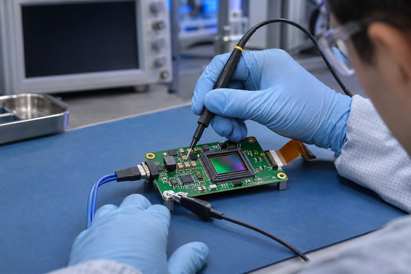
The observed symptom can help identify which part of the PCB should be checked first.
| Observed Problem | Possible PCB-Related Cause | Recommended Check |
|---|---|---|
| Horizontal bands or periodic image artifacts | Power ripple or periodic interference | Measure sensor supply rails and compare with frame or row timing |
| Noise changes with power load | Supply instability or ground coupling | Check voltage at the sensor power pins |
| MIPI frame errors or intermittent data loss | Impedance discontinuities, skew, or channel loss | Check differential routing, vias, connectors, and interface diagnostics |
| Image artifacts vary with digital activity | Clock coupling or EMI | Check clock routing and switching activity |
| Problems appear after a PCB revision | Changes in stackup, return paths, or placement | Compare PCB revisions and manufacturing specifications |
Power integrity is especially important for CMOS image sensors. Many sensors require separate analog, digital-core, and interface power supplies. Disturbances on sensitive analog rails can contribute to image noise, banding, or reduced dynamic range.
Ground interference occurs when sensitive circuitry shares return impedance with high-current or fast-switching circuits. The resulting voltage disturbances can affect sensor references and increase unwanted coupling.
However, not every image artifact originates from the PCB. Sensor fixed-pattern noise, illumination flicker, temperature, and image-processing settings can produce similar symptoms.
Electrical measurements should therefore be compared with the observed image behavior before modifying the PCB layout.
How to Reduce Signal Noise in an Image Sensor PCB?
Reducing image sensor PCB noise requires stable power delivery, continuous return paths, properly controlled high-speed routing, and consistent PCB manufacturing. The following measures address the main electrical causes without introducing unnecessary design complexity.
1. Improve sensor power integrity
Place decoupling capacitors close to the corresponding sensor power pins and keep power-to-ground current loops short.
- Follow the sensor datasheet for capacitor values and power sequencing.
- Keep switching regulator current loops compact.
- Use appropriate filtering or low-noise regulation for sensitive power rails.
- Measure supply ripple and transient response at the sensor pins during operation.
Avoid adding ferrite beads without evaluating their impedance and interaction with the power network. Poorly selected filtering components can introduce resonance or worsen transient performance.
2. Maintain continuous ground reference planes
Critical signals need predictable return-current paths.
- Route high-speed signals over continuous reference planes.
- Avoid crossing gaps or splits in ground planes.
- Minimize unnecessary signal-layer transitions.
- Provide suitable return-current connections when changing layers.
A short signal route can still create interference when its return current must travel around a large reference-plane opening.
3. Control MIPI CSI-2 routing
MIPI D-PHY interfaces commonly use controlled differential impedance, but the exact requirement depends on the connected devices.
For example, published AMD D-PHY guidelines include 95 Ω ±10% and 100 Ω ±10% differential impedance requirements for different device families. These values should not be treated as interchangeable.
When routing MIPI signals:
- Maintain the specified differential impedance.
- Control within-pair skew according to the device requirements.
- Minimize unnecessary vias and abrupt trace transitions.
- Separate high-speed data pairs from noisy switching circuits.
- Include FPC connectors and cables in the complete channel assessment.
4. Reduce EMI and clock interference
Keep switching nodes, clock generators, and sensitive analog supply paths separated where practical. Avoid long parallel routing between aggressive digital signals and sensitive circuits.
Signal spacing should be determined according to operating speed, trace geometry, reference planes, and the expected interference level.
5. Maintain the approved impedance during fabrication
Finished trace width, copper thickness, and dielectric thickness directly affect PCB impedance.
For controlled-impedance boards, specify the target value, tolerance, relevant signal layers, and approved stackup. Representative impedance coupons can be used where required to verify the fabricated construction.
Controlled PCB fabrication helps preserve the electrical characteristics required for stable sensor operation, reducing the risk of signal problems introduced by manufacturing variations.
What Image Sensor PCB Design Mistakes Can Cause Manufacturing Failures?
Fine-pitch pad errors, unsuitable via structures, incompatible trace dimensions, and incorrect mechanical tolerances are common causes of image sensor PCB manufacturing problems.
These issues should be corrected before the manufacturing files are released.
1. Incorrect sensor pad and solder-mask geometry
Pads that do not match the sensor package can cause solder bridging, insufficient solder joints, or placement problems.
Check the component manufacturer’s recommended footprint, pad dimensions, solder-mask openings, and spacing between adjacent pads.
2. Unfilled vias inside solderable pads
Open vias can allow solder to flow into the hole during reflow, reducing the solder available for the component joint.
Where via-in-pad is required, specify resin filling, planarization, and copper capping as applicable. Ordinary solder-mask plugging is not equivalent to filled and plated-over via processing.
3. Trace width and spacing incompatible with copper thickness
Fine-line capability depends on copper weight and the manufacturing process.
A trace width suitable for a thin copper layer may not be practical with significantly thicker copper. The complete construction must be reviewed before selecting the minimum available trace/spacing values.
4. Conflicting PCB thickness and impedance requirements
A fixed finished thickness restricts the available dielectric construction.
If the selected trace geometry cannot meet the required impedance within the specified thickness, the stackup or routing dimensions must be adjusted before fabrication.
5. Mechanical dimensions that do not match the sensor assembly
Incorrect mounting-hole positions, board dimensions, or flatness requirements can prevent accurate installation.
Define critical mechanical dimensions and acceptable tolerances in the fabrication drawing.
A free DFM check helps identify these conflicts before production, reducing the risk of rejected boards, unnecessary PCB revisions, and assembly rework.
How Are High-Density Image Sensor PCBs Manufactured?
High-density image sensor PCBs are produced through precision circuit fabrication, multilayer lamination, HDI drilling, controlled copper plating, and accurate surface finishing. Each process must preserve the approved routing geometry and reliable interlayer connections.
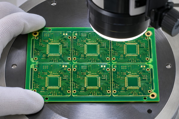
The most important manufacturing stages are:
1. Fine-Line Circuit Fabrication
Circuit imaging and etching define the conductor geometry. Fine-pitch image sensor PCBs require consistent trace width, spacing, and copper clearance, particularly around dense component footprints.
The process must also preserve the approved trace geometry for controlled-impedance connections.
2. Multilayer Registration and Lamination
Inner layers are aligned and laminated according to the approved stackup.
Accurate registration is necessary when dense interconnections use small pads or narrow annular rings. Dielectric thickness must also remain within the specified manufacturing limits.
3. HDI Microvia Formation
Laser drilling supports dense interconnections between selected layers where conventional through-holes consume excessive routing space.
Microvias are metallized and plated to establish reliable electrical connections. Stacked and staggered structures require suitable layer construction, with filling and capping where specified.
4. Solder Mask and Surface Finishing
Precise solder-mask registration is important for closely spaced sensor pads.
The surface finish must be compatible with the intended component package and soldering process. ENIG, ENEPIG, and OSP are possible options depending on the approved assembly requirements.
5. Mechanical Processing and Final Inspection
PCB profiling and drilling must meet the specified board dimensions and mechanical tolerances.
Finished boards undergo appropriate electrical and dimensional inspection before assembly or shipment.
HDI technology should be used when the package density and routing requirements justify it. If a conventional multilayer PCB can meet the electrical and mechanical specifications, additional HDI processing may not be necessary.
How Can Image Sensor PCB Assembly Defects Be Reduced?
Image sensor PCB assembly defects can be reduced through controlled solder paste printing, accurate component placement, package-specific reflow conditions, and protection against ESD and optical contamination.
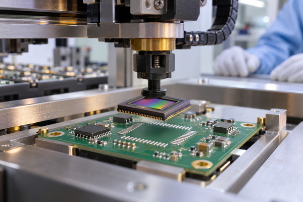
These controls are particularly important for CMOS sensors using fine-pitch packages or sensitive optical structures.
1. Control solder paste volume
Fine-pitch LGA, BGA, and CSP packages require stencil openings matched to the approved land pattern.
Excessive paste can produce bridging or package movement, while insufficient paste may cause open joints.
SPI can identify unsuitable deposits before expensive image sensor components are placed.
2. Maintain placement accuracy
Sensor orientation, pad alignment, and package coplanarity must match the assembly drawing.
Placement equipment should use handling methods compatible with the sensor package and avoid applying damaging pressure to optical surfaces.
3. Follow the sensor’s soldering requirements
The approved reflow profile depends on package construction, moisture sensitivity, and allowable thermal exposure.
Not all image sensors support conventional SMT reflow. The component manufacturer’s soldering instructions must be checked before assembly.
4. Prevent ESD and optical contamination
Dust, flux residue, fingerprints, and electrostatic discharge can damage sensitive image sensor assemblies.
Important controls include:
- ESD-safe storage and component handling.
- Protection of optical windows against contact and particles.
- Cleaning methods approved for the sensor package.
- Suitable protective packaging after assembly.
5. Inspect solder joints before final integration
AOI can identify visible placement and soldering defects. X-ray inspection may be required for selected hidden joints.
These inspections help identify assembly problems before the PCB enters later manufacturing stages.
For high-value image sensors, preventing defects before reflow also reduces unnecessary thermal rework and the risk of component damage.
What Quality Tests Should Image Sensor PCBs Pass Before Delivery?
Image sensor PCBs should pass electrical, dimensional, and fabrication inspections. Assembled boards require additional soldering and functional verification according to the customer’s approved acceptance criteria.
The inspection plan should cover the following areas:
- PCB Electrical Testing: Flying-probe or fixture testing checks for open and short circuits against the approved netlist.
- Controlled-Impedance Testing: Representative test coupons verify impedance against the specified target and tolerance.
- Dimensional Inspection: Board thickness, outline, mounting holes, and critical dimensions are checked against the fabrication drawing.
- Copper and Via Inspection: Copper measurements and applicable microsection analysis assess plated interconnections and internal construction.
- SMT Inspection: SPI, AOI, and X-ray identify solder paste, placement, and applicable solder-joint defects.
- Functional Testing: Customer-defined procedures may verify sensor initialization, supply voltages, interface communication, and image-data transmission.
- Production Traceability: Manufacturing revisions, material information, inspection records, and production batches are maintained according to the agreed quality requirements.
For a CMOS image sensor PCB, a passing electrical test does not guarantee acceptable image quality.
Dark-frame noise, defective pixels, image artifacts, and dropped-frame behavior require appropriate sensor hardware, software, lighting conditions, and defined acceptance criteria.
Customers can specify the required test reports, functional test procedures, and inspection standards before production. This ensures that the manufacturing and testing scope matches the actual application requirements.
Case Study: Custom Image Sensor PCB Manufacturing and Assembly
Project Background
A customer serving the Thailand security-camera market required a custom 4-layer PCB for a camera module. The project involved controlled signal transmission, SMT assembly, PCB cleanliness, and preparation for product validation.
The intended operating environment also raised concerns about heat and humidity, making material suitability and assembly protection important considerations.
Project Requirements
The customer provided the following PCB manufacturing and assembly specifications:
- PCB Layers: 4 layers
- Base Material: FR-4, Tg130
- Finished Thickness: 1.6 mm ±10%
- Copper Weight: 1 oz
- Signal Requirement: 14 mil trace width and 50 Ω single-ended impedance
- Surface Finish: ENIG
- Solder Mask / Silkscreen: Black / White
- Assembly: SMT
- Quality Requirements: No visible solder balls or residue; individual-board packaging
Manufacturing Challenges and Solutions
Three manufacturing issues required particular attention:
- Controlled Impedance: The specified 50 Ω single-ended signal required consistency between trace width, copper thickness, dielectric construction, and the approved stackup. EBest Circuit reviewed these parameters and included an impedance test coupon and reporting requirement in the production plan.
- SMT Assembly and Cleanliness: Small components and connector areas required accurate assembly preparation. EBest Circuit reviewed the BOM, placement files, connector locations, and SMT instructions, with post-assembly cleanliness inspection and individual packaging included in the manufacturing requirements.
- Environmental Suitability: The potential exposure to heat and humidity required evaluation of the Tg130 FR-4 construction. Additional measures, including conformal coating, enclosure sealing, and connector protection, were identified for confirmation against the finished product’s operating conditions.
Project Output Results
The manufacturing review established a defined production plan covering the 4-layer PCB construction, 50 Ω single-ended impedance requirement, SMT assembly documentation, cleanliness criteria, and individual packaging specifications.
An impedance test coupon and report were included in the verification plan, while the assembly review clarified the component placement and inspection requirements.
These preparations provided a consistent manufacturing basis for prototype validation and subsequent small-batch production, reducing the risk of rework caused by unclear or conflicting production specifications.
The project’s signal requirement was 50 Ω single-ended impedance, which must not be confused with the differential-impedance requirements used by many MIPI D-PHY interfaces.
Why Choose EBest Circuit for Image Sensor PCB Manufacturing?
EBest Circuit helps customers reduce image sensor PCB manufacturing risks, avoid unnecessary rework, and maintain consistent quality from prototypes to repeat production.
Our services address the problems that most directly affect manufacturing reliability:
- Reduce PCB-Related Signal Noise Risks: Controlled-impedance fabrication and approved stackup construction help maintain the electrical characteristics required for stable signal transmission, reducing the risk of manufacturing variations affecting high-speed interfaces.
- Avoid Costly PCB Revisions: Our free DFM check identifies potential problems with fine-pitch pads, trace spacing, microvias, board thickness, and mechanical requirements before fabrication. This helps prevent avoidable manufacturing changes and rejected boards.
- Reduce Fine-Pitch Assembly Defects: We provide SMT assembly with applicable SPI, AOI, and X-ray inspection. Sensor-specific soldering and handling requirements can be included in the approved assembly process to reduce soldering failures and component damage.
- Simplify Manufacturing and Component Procurement: PCB fabrication, approved component sourcing, SMT assembly, and agreed testing can be coordinated through one supplier, reducing communication errors between separate manufacturing providers.
- Support Consistent Prototype and Volume Production: Approved fabrication files, BOM revisions, assembly instructions, and inspection criteria provide a controlled manufacturing baseline for sample builds, small batches, and repeat orders.
EBest Circuit lists ISO 9001, ISO 13485, IATF 16949, and AS9100D quality-management certifications. Applicable certificate copies, manufacturing scope, and project-specific quality records can be confirmed during supplier qualification.
For industrial camera electronics, machine vision systems, security devices, and medical imaging equipment, we manufacture and assemble custom image sensor PCBs according to customer-approved specifications.
FAQs About Image Sensor PCB
Q1: Is a black solder mask necessary for an image sensor PCB?
A1: No. Black solder mask may be specified to manage reflections in certain optical assemblies or meet product appearance requirements. It does not directly reduce electrical noise. The final color should follow the product’s optical and manufacturing specifications.
Q2: Can an image sensor PCB be supplied without the sensor installed?
A2: Yes. EBest Circuit can supply bare PCBs, partially assembled boards, or complete PCBAs. If the sensor will be installed later, the surface finish, packaging, storage, and subsequent soldering conditions should be specified.
Q3: Can EBest Circuit assemble customer-supplied image sensors?
A3: Yes, subject to component and process review. Customers should provide the sensor part number, package type, quantity, packing format, handling requirements, and approved soldering instructions.
Q4: Does image sensor PCB assembly always require a cleanroom?
A4: No. The required cleanliness level depends on the sensor package, exposed optical surfaces, and acceptance criteria. Standard packaged sensors and exposed optical assemblies may require different handling environments.
Q5: Can EBest Circuit sign an NDA for an image sensor PCB project?
A5: Yes. Customers can request an NDA before sharing confidential Gerber files, BOMs, sensor specifications, or mechanical drawings. Confidentiality requirements can be agreed upon before technical review.
Q6: Can image sensor PCBs use customer-specified components?
A6: Yes. EBest Circuit supports approved BOM sourcing, customer-supplied components, and hybrid sourcing arrangements. Any component substitution requires customer approval, particularly for image sensors and other critical devices.
Q7: Can the same image sensor PCB design be used for prototypes and volume production?
A7: Yes, provided the design has been validated and the manufacturing requirements remain appropriate for the production quantity. Changes affecting the stackup, sensor package, or critical materials may require additional approval or testing.
Q8: What information is required for an image sensor PCB quotation?
A8: Provide the Gerber or ODB++ files, drill data, stackup, board thickness, copper weight, surface finish, controlled-impedance requirements, quantity, required delivery date, and delivery location. For assembly, include the BOM, pick-and-place file, sensor datasheet, assembly drawing, and testing requirements.
Are signal noise, unstable MIPI transmission, or fine-pitch assembly defects delaying your image sensor PCB project? These problems can lead to repeated PCB revisions, failed inspections, and unnecessary production delays.
EBest Circuit can help reduce PCB-related signal noise risks and assembly defects through controlled-impedance manufacturing, precision HDI fabrication, reliable SMT assembly, and project-specific inspection. Whether you need a CMOS image sensor PCB prototype or repeat production, we can help identify manufacturing risks before they cause rework.
Send your Gerber files, BOM, quantity, and technical requirements to sales@bestpcbs.com for a free DFM check and custom manufacturing quotation. Let EBest Circuit help you prevent avoidable defects, maintain consistent PCB quality, and move your image sensor PCB project into production with confidence.