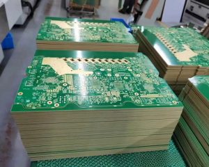
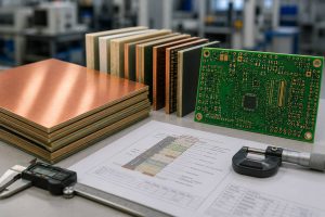
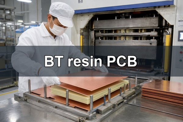
A BT resin PCB uses Bismaleimide-Triazine (BT) resin-based laminate for applications requiring thermal stability, controlled electrical performance, and dimensional accuracy. Its stackup must account for dielectric thickness, copper geometry, and material properties, while manufacturing requires suitable lamination and drilling processes.
For thin multilayer boards, small changes in dielectric spacing, copper distribution, or processing conditions can affect impedance and warpage. EBest Circuit provides custom PCB manufacturing and DFM support to help customers review these requirements before fabrication.
What Should You Consider Before Designing a BT Resin PCB Stackup?
Define the BT laminate grade, layer count, finished thickness, and electrical requirements before arranging the copper layers. These specifications determine whether the stackup can meet the required electrical and mechanical performance.
Four areas deserve attention:
- BT Laminate: Specify the Bismaleimide-Triazine material grade and compatible core and prepreg. Different formulations have different dielectric properties, thickness options, and processing requirements.
- Board Construction: Confirm the layer count, finished thickness, and copper weight to determine the space available for dielectric layers.
- Electrical Requirements: Identify signal layers, reference planes, target impedance, and operating frequency before selecting dielectric spacing.
- Mechanical Requirements: Define via structures, dimensional tolerances, and allowable warpage, especially for thin boards.
The laminate grade should be confirmed before finalizing the impedance geometry. Replacing the material later may change the required trace dimensions or dielectric construction. The selected grade’s Bismaleimide-Triazine resin properties should match the project’s electrical and thermal requirements.
What Does a 4-Layer BT Resin PCB Stackup Look Like?
A 4-layer BT resin PCB stackup can use two outer signal layers separated by internal ground and power planes. BT-based core material and compatible prepregs provide electrical insulation and mechanical support.
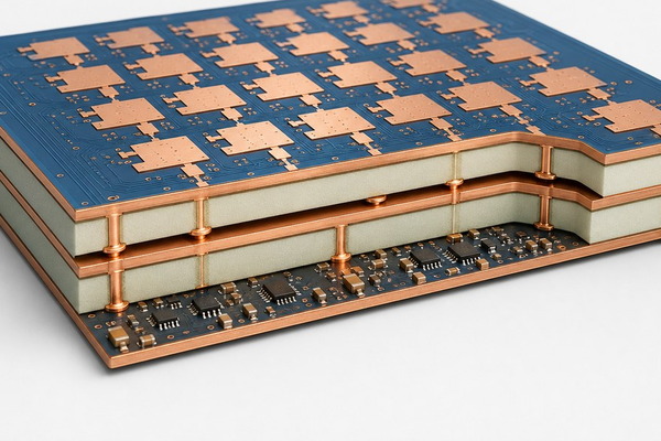
A four-layer construction can use the following layer arrangement and nominal dimensions.
| Layer or Material | Thickness | Function |
|---|---|---|
| L1 – Signal Copper | 18 µm nominal | Signal routing and component pads |
| BT Prepreg | 0.10 mm cured target | Dielectric between L1 and L2 |
| L2 – Ground Plane | 18 µm nominal | Signal reference and return path |
| BT Core | 0.20 mm dielectric | Structural support and insulation |
| L3 – Power Plane | 18 µm nominal | Power distribution |
| BT Prepreg | 0.10 mm cured target | Dielectric between L3 and L4 |
| L4 – Signal Copper | 18 µm nominal | Bottom-side signal routing |
The specified dielectric thicknesses total 0.40 mm, while four nominal 18 µm copper layers contribute 0.072 mm. Their combined nominal thickness is approximately 0.472 mm, before additional outer-layer plating, solder mask, and finishing effects.
The finished thickness depends on cured prepreg dimensions, finished copper thickness, and fabrication tolerances. Core and prepreg thicknesses must also be available in the selected BT laminate system.
The L1–L2 dielectric spacing affects top-layer impedance, while L4 can use L3 as a reference where the plane provides a suitable continuous return path. Copper coverage and plane continuity must also be considered when assessing electrical performance and mechanical balance.
How Do Copper Thickness and Dielectric Spacing Affect BT PCB Impedance?
Increasing dielectric spacing generally raises microstrip impedance, while increasing trace width or copper thickness generally lowers it. The actual impedance depends on trace geometry and the dielectric constant (Dk) of the selected Bismaleimide-Triazine laminate.
| Parameter Change | Impedance Effect | Design Adjustment |
|---|---|---|
| Increase Dielectric Thickness | Generally increases | Adjust trace width if necessary |
| Increase Trace Width | Decreases | Check spacing and routing clearance |
| Increase Copper Thickness | Generally decreases | Calculate using finished conductor geometry |
| Increase Dk | Decreases | Recalculate for the selected laminate grade |
| Change Etched Trace Geometry | Changes impedance | Account for finished trace width and profile |
Consider a 50 Ω single-ended microstrip with 0.10 mm dielectric spacing. If the spacing is reduced to 0.075 mm while the conductor geometry remains unchanged, impedance will generally decrease.
Restoring the target impedance may require a narrower trace. However, the reduced width must remain within the manufacturer’s achievable fabrication limits.
Before finalizing controlled-impedance routing:
- Confirm Dk: Use material data at the relevant operating frequency.
- Calculate Impedance: Model the finished copper geometry and dielectric spacing.
- Check Trace Dimensions: Verify minimum line width, spacing, and manufacturing tolerances.
- Specify Test Requirements: Define target impedance, tolerance, and verification method.
For high-frequency applications, dissipation factor (Df) and copper roughness also affect transmission loss. A trace that meets its impedance target may still have unacceptable insertion loss.
What Trace and Via Design Rules Apply to BT Resin PCBs?
BT resin PCB routing limits depend on copper thickness, dielectric construction, and hole-processing capability. The resin type alone does not determine the minimum trace width or via diameter.
- Trace Width and Spacing: Fine-line capability depends on copper thickness, imaging accuracy, and etching control. Specify the required finished conductor dimensions.
- Through-Hole Vias: Drill diameter, aspect ratio, annular ring, and plating thickness must be compatible with the finished board thickness.
- Blind Vias and Microvias: Confirm that the selected BT dielectric supports the required laser-drilling and metallization processes. Via depth, diameter, and capture pad dimensions must be evaluated together.
- BGA Fanout: Review pad pitch, available routing channels, and via placement before selecting the interconnection structure.
Reducing via diameter can create additional routing space, but the smaller via must still provide reliable interlayer connections.
For dense multilayer layouts, the smallest trace features and any nonstandard via structures should be reviewed against the selected BT laminate and fabrication method. Semiconductor package-substrate design rules should not be applied automatically to conventional multilayer BT resin PCBs.
How Can You Design a BT Resin PCB Stackup to Reduce Warpage?
A symmetrical dielectric construction, balanced copper distribution, and suitable board thickness help reduce warpage in thin BT resin PCBs. These measures limit uneven thermal and mechanical stresses that can cause bending during manufacturing or assembly.
Five design measures are particularly useful:
- Keep the Stackup Symmetrical: Arrange corresponding copper and dielectric layers around the board center wherever practical.
- Balance Copper Coverage: Reduce unnecessary differences in copper density between opposite layers without compromising electrical performance.
- Consider Material CTE: Select a Bismaleimide-Triazine laminate with thermal expansion and dimensional stability appropriate for the application.
- Check Board Thickness: Very thin boards have lower bending stiffness. Increasing thickness where the product allows can improve mechanical stability.
- Set Flatness Requirements: Define the acceptable bow, twist, or application-specific warpage limits in the fabrication drawing.
For boards exposed to lead-free reflow, thermal expansion mismatch and uneven copper distribution can increase deformation during heating. The specified flatness requirements should reflect the intended assembly conditions.
How Are Bismaleimide-Triazine PCBs Manufactured?
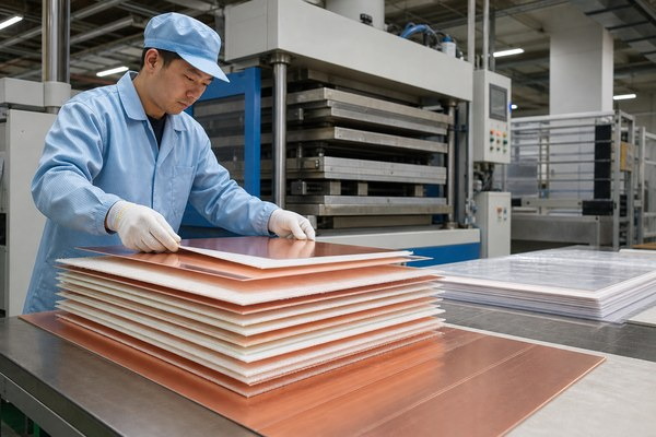
BT resin PCB manufacturing requires material-specific control during lamination, drilling, and hole preparation. These operations must match the selected Bismaleimide-Triazine laminate rather than relying on a universal processing recipe.
Step 1: BT Laminate Preparation
Confirm the BT core, prepreg, copper thickness, and material grade. Storage and moisture handling follow the laminate supplier’s requirements.
Step 2: Inner-Layer Circuit Formation
Inner copper layers are patterned and inspected. Compatible copper surface treatment prepares them for reliable bonding during lamination.
Step 3: Multilayer Lamination
BT cores and prepregs are aligned and pressed under controlled conditions. Curing temperature, pressure, and time must match the resin system to achieve the required bonding and dielectric thickness.
Step 4: Drilling and Desmear
Mechanical drilling forms through-holes, while suitable laser processes may create microvias. Resin smear must be removed from exposed inner-layer copper before metallization. Plasma or compatible chemical treatments are selected according to the BT formulation.
Step 5: Copper Metallization and Circuit Formation
Prepared holes are metallized and plated. Outer-layer circuits are formed, with finished copper thickness and trace geometry controlled against the approved fabrication specifications.
Step 6: Surface Finish and Inspection
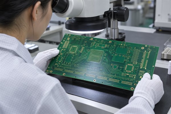
Solder mask, the specified surface finish, and profiling are completed. Inspection covers layer registration, hole metallization, dimensions, and electrical continuity, with impedance or warpage checks where required.
BT Resin PCB Manufacturing Example: A Thin 6-Layer Stackup
A thin six-layer BT resin PCB with controlled-impedance routing requires coordinated checks of dielectric thickness, copper balance, and via geometry before fabrication. Consider the following engineering scenario for a compact communication module.
Project Background
The proposed board has six copper layers, a target finished thickness of 0.80 mm, and 50 Ω single-ended signal routing. Bismaleimide-Triazine laminate is specified for its required electrical and dimensional characteristics.
Manufacturing Requirements and Challenges
The limited board thickness leaves little room for the dielectric layers, copper, and plating. Uneven copper distribution can increase warpage risk, while changing dielectric spacing to meet the thickness target may alter impedance. Fine-pitch connections also require confirmation of the via structure.
Engineering Solution
The proposed manufacturing review addresses three issues:
- Stackup Adjustment: Check the available BT core and prepreg constructions, maintain a balanced layer arrangement, and recalculate impedance using the final dielectric spacing.
- Copper and Via Review: Compare copper distribution between corresponding layers and verify that the required via dimensions are compatible with the board thickness.
- Manufacturing Verification: Specify finished thickness, impedance tolerance, flatness limits, electrical testing, and any required structural inspection.
Expected Verification Results
The design can proceed to fabrication approval when the material construction and manufacturing limits have been confirmed. The finished boards must then be checked against the specified 0.80 mm thickness target, 50 Ω impedance requirement, and agreed flatness limits.
These are proposed design and acceptance requirements for an illustrative engineering scenario, not measurements from a completed production lot.
Why Choose EBest Circuit for BT PCB Manufacturing?
EBest Circuit provides PCB manufacturing, DFM support, and documented quality control to help customers move from approved stackup specifications to production.
- Material and Stackup Review: Review BT laminate specifications, copper construction, dielectric thickness, and manufacturing compatibility before fabrication.
- DFM Support: Identify potential fabrication problems involving trace dimensions, via structures, layer alignment, and board thickness.
- Engineering Coordination: Support technical communication between project review, manufacturing, and quality control. For projects that also require PCBA, EBest Circuit’s 1+3 technical team covers PE, DFM, Process, and Quality functions.
- Quality and Traceability: EBest Circuit maintains ISO 9001, ISO 13485, IATF 16949, and AS9100D certifications, with applicable manufacturing records retained for up to 15 years.
- Prototype to Volume Production: Support sample fabrication and repeat production using approved manufacturing specifications.
BT laminate availability and specialized fabrication capabilities are evaluated for each project, allowing material and processing restrictions to be identified before production.
Send your BT resin PCB manufacturing requirements to sales@bestpcbs.com for DFM review and a quotation.
What Do You Need for a BT Resin PCB Manufacturing Quote?
Provide the fabrication files, BT laminate specification, stackup, and production requirements. These details allow the manufacturer to evaluate material availability and fabrication feasibility.
- Fabrication Files: Gerber or ODB++, NC drill files, and fabrication drawing.
- BT Material: Manufacturer, laminate grade, core, prepreg, and approved substitutions.
- Stackup: Layer count, finished thickness, copper thickness, and dielectric spacing.
- Electrical Specifications: Impedance targets, tolerances, and required electrical tests.
- Manufacturing Requirements: Minimum trace dimensions, via structures, surface finish, and flatness limits.
- Order Details: Quantity, delivery requirements, and shipping destination.
If the BT laminate grade has not been finalized, provide the required electrical, thermal, and mechanical specifications for manufacturing review.
FAQ About BT Resin PCB Manufacturing
Q1: Can a BT resin PCB have more than four layers?
A1: Yes. Multilayer constructions are possible when the selected BT core, prepreg, and fabrication process support the required structure.
Q2: Can BT resin laminate be combined with other dielectric materials?
A2: Yes, in a qualified hybrid construction. Lamination compatibility, CTE, adhesion, and dielectric properties must be evaluated.
Q3: Does BT resin require a special surface finish?
A3: Not necessarily. ENIG, ENEPIG, and other compatible finishes can be selected according to soldering, bonding, and product requirements.
Q4: Can a BT resin PCB withstand lead-free reflow?
A4: Many BT laminate grades support lead-free assembly. Acceptable reflow conditions depend on the material, board construction, and moisture condition.
Q5: Should BT prepreg be baked before lamination?
A5: Follow the supplier’s prepreg storage and handling requirements. Unapproved baking may affect the partially cured resin’s processing behavior.
Q6: How can BT laminate traceability be verified?
A6: Request material identification, supplier records, and applicable lot traceability linked to the manufacturing order.
Q7: What can cause delamination in a BT resin PCB?
A7: Possible causes include moisture, inadequate bonding, incompatible processing conditions, or excessive thermal stress. The actual cause requires inspection and failure analysis.
Q8: Can an approved BT laminate be replaced with another grade?
A8: Only after comparing dielectric properties, thermal expansion, available thicknesses, and processing compatibility, followed by customer approval.
Conclusion
A reliable BT resin PCB requires a suitable Bismaleimide-Triazine laminate, a balanced stackup, and compatible manufacturing processes. Dielectric spacing, copper geometry, via construction, and warpage requirements should be established before fabrication to reduce production risks.
Need custom BT resin PCB manufacturing? EBest Circuit provides DFM review and PCB fabrication support from prototype through production. Send your Gerber files, stackup, BT laminate specifications, and order quantity to sales@bestpcbs.com for manufacturing feasibility review and quotation.