A bird feeder camera needs a PCB assembly that keeps image capture, wireless communication and battery power working together outdoors. For OEM brands, dependable production means more than mounting the right components: camera connectors must remain secure, charging circuits must match the battery, and each assembled board needs a test plan tied to its actual functions.
At EBest Circuit (Best Technology), we support PCB fabrication, component sourcing, SMT and through-hole assembly, inspection and project-specific functional testing. Our turnkey and consignment options fit both new hardware builds and established designs moving into production. To discuss your bird feeder camera PCBA requirements, visit our Contact Us page and complete the enquiry form at the bottom of the page.
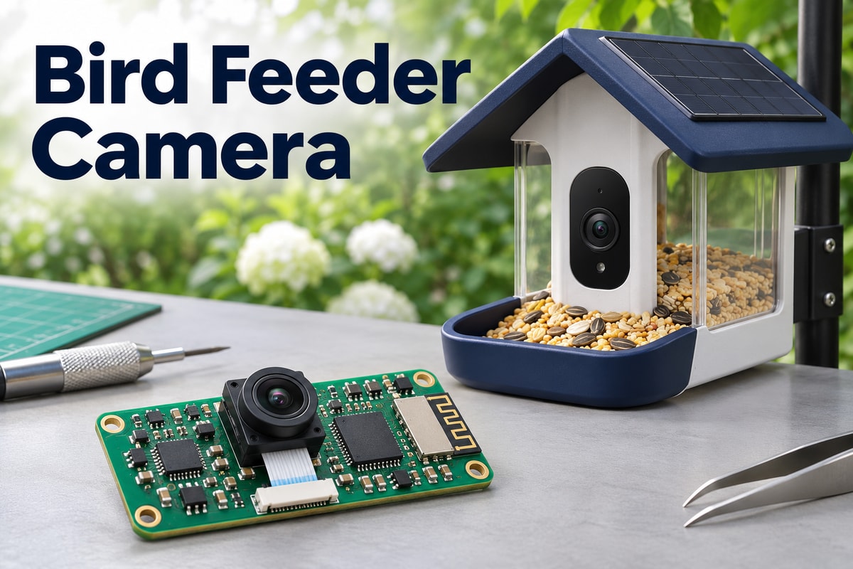
Smart Bird Feeder PCBA Manufacturing Capabilities
We can manufacture and assemble the control, communication and power boards used in smart bird feeder designs. The scope can cover a single integrated board or separate boards connected to camera, antenna and battery modules.
| Manufacturing item | Capability | Relevance to the assembly |
|---|---|---|
| Small SMD components | Down to 01005 package size | Compact filtering, bias and decoupling circuits |
| BGA assembly | Minimum pitch of 0.25 mm | Dense processor and memory packages |
| Assembly processes | SMT, through-hole and mixed assembly | ICs, passives, headers and power connectors |
| Component supply formats | Reels, cut tape, tubes, trays and loose parts | Prototype quantities and production packaging |
| Soldering equipment | Nitrogen reflow and wave soldering | Process selection for different package and connector types |
| Inspection and testing | SPI, AOI, X-ray and functional testing | Paste deposits, solder joints and circuit operation |
Minimum package and pitch capabilities require a review of the actual footprint, board layout and assembly process. They do not mean every design should use the smallest available parts. Space for connectors, antenna clearance and test access can be more valuable than further component miniaturization.
Our supply options also accommodate different levels of customer involvement. With full turnkey assembly, we procure the BOM and coordinate board manufacturing and assembly. Partial turnkey assembly allows you to supply selected items, such as a proprietary camera module, while we procure the remaining components. Consignment assembly suits customers who already control their complete component supply.
Solar Powered Bird Feeder Camera PCB Assembly
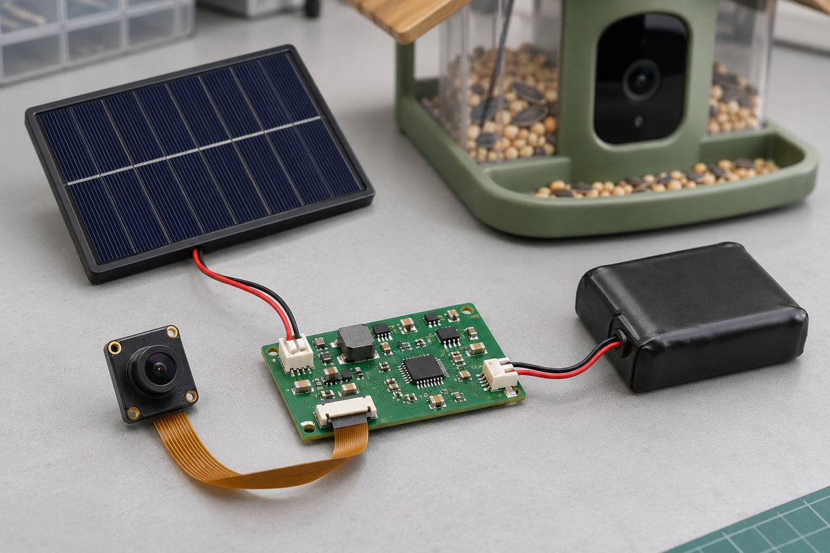
Solar-powered designs need an assembly process that preserves the charging circuit’s electrical settings and the battery connection’s mechanical reliability. The panel, charger, battery and system load must operate as a matched power system.
A panel’s rated power alone does not determine charging performance. Available sunlight changes during the day, while recording and wireless transmission create changing loads. A charger with suitable input regulation and power-path control can manage these conditions, but its operating limits must match the selected panel and cell chemistry.
For assembly, three areas deserve particular attention.
- Charging configuration. Resistor values, temperature-sensing components and battery-voltage settings affect how the charger behaves. Similar-looking parts with different values can change its operation.
- Power connections. Battery and panel connectors need correct polarity, pin assignment and soldering. Cable loads should be supported by the mechanical design rather than carried entirely by solder joints.
- Thermal performance. Power-device pads and heat-spreading copper must follow the design requirements. Poor solder coverage can interfere with heat transfer even when the board initially powers up.
For a suitable design, the functional test can include charging under defined input conditions, operation from the battery and transitions between power sources. These tests provide repeatable production checks; they do not establish a fixed number of outdoor operating days.
Wireless Bird Feeder Camera Module Assembly
Wireless camera assemblies can use a ready-made radio module or a radio circuit implemented directly on the main PCB. The distinction changes the manufacturing workload and the RF validation needed.
| Approach | Assembly considerations | RF work still required |
|---|---|---|
| Ready-made wireless module | Module pads, orientation, reflow limits and antenna clearance | Host-board and enclosure performance verification |
| Radio circuit on the main PCB | RF components, matching network, controlled geometry and grounding | Circuit tuning and validation for the complete implementation |
A module can consolidate several RF components into one purchased part, but it does not remove the need to evaluate the finished product. Batteries, cables, metal fasteners and the feeder enclosure can affect the antenna environment.
During production preparation, the module’s assembly instructions should be carried into the placement, soldering and inspection plan. Camera ribbon connectors also need attention: contact orientation, latch access and cable routing must suit the enclosure and assembly sequence.
Our work with wireless module PCB manufacturing is relevant to these board-level interfaces. Wi-Fi frequency support, image resolution and bird-identification functions remain dependent on the selected hardware and software architecture.
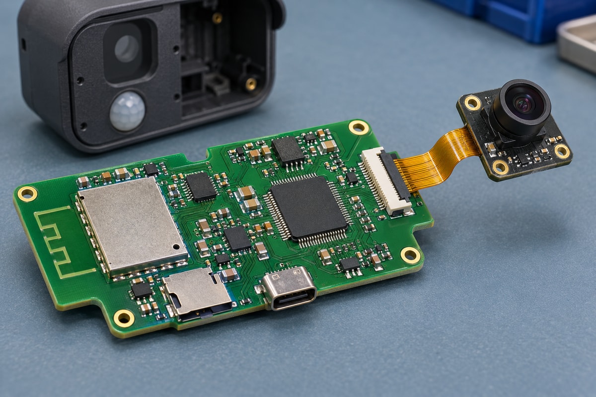
Smart Bird Feeder Camera Prototypes and Volume Production
A prototype build establishes whether the design can be assembled and tested consistently. Volume production then uses the approved board revision, BOM and test configuration as a controlled baseline.
Prototype assembly gives the hardware team access to assembled boards for camera bring-up, power measurements and enclosure integration. At this stage, connector orientation, programming access and fixture contact points are easier to improve than after a production batch has started.
A pilot build helps evaluate repeatability. It can reveal problems that a few hand-handled samples may miss, such as inconsistent cable seating, difficult depanelization or an unnecessarily slow test sequence.
Volume production needs stable materials and instructions. A replacement camera module or radio module may change pin assignments, firmware compatibility or antenna behavior. Such changes deserve engineering review before they enter the build, even if the replacement appears mechanically similar.
At EBest Circuit, PCB fabrication, component procurement and assembly can be coordinated within one service scope. This helps carry approved changes from the prototype into the production BOM and manufacturing documents.
Bird Feeder Camera PCBA Testing and Quality Control
Reliable quality control combines solder-process inspection with functional checks. A visually acceptable board can still contain an incorrect component value or fail during image capture, so inspection alone cannot replace operation under defined conditions.
SPI examines solder-paste deposits before reflow. AOI checks visible assembly features, while X-ray supports inspection of hidden solder connections. Functional testing then evaluates the circuit using the required firmware, fixtures and peripherals.
The following checks can form part of a bird feeder camera production test plan, depending on the design and agreed coverage.
| Function | Example production check | Defined test condition |
|---|---|---|
| Camera interface | Start capture and verify image output | Approved sensor/module, firmware and test target |
| Wireless connection | Connect and transfer data | Known access point, channel and RF environment |
| Solar charging input | Verify charging behavior and status | Controlled input source and battery condition |
| Battery operation | Measure sleep and active current | Specified firmware state and enabled peripherals |
| Event capture | Trigger the fitted sensor and record a response | Defined stimulus and timing limit |
| Local storage | Write and read a test file | Approved storage device and interface |
The electrical test plan should distinguish normal operating modes. A sleep-current result is meaningful only if the camera, wireless connection and status indicators are in their specified states.
Outdoor protection requires a separate product-level evaluation. Board cleanliness and suitable protective processes matter, but an enclosure’s IP rating cannot be assigned to a bare PCBA. Connectors, seals and the completed housing determine the final ingress-protection performance.
PCBA Case Study: Lessons for a Smart Bird Feeder with Camera Project
EBest Circuit has manufactured PCB and PCBA products for bird feeder camera applications. Our camera-electronics manufacturing experience also includes a Camera FPGA Board Rev2.0 project with specific requirements for connector fit, rigid-flex construction and controlled impedance. This case focuses on that board’s manufacturing requirements and their relevance to compact camera products.
Application
The camera FPGA board combined rigid circuit sections with a flexible interconnection. Its construction brought high-speed signal routing and mechanical interfaces into the same manufacturing job—two closely related considerations when electronics must fit inside a compact camera enclosure.
Challenge
The through-hole connector had a 1.65 mm tail length, and the project instructions identified board thickness above 1.65 mm as a connection and stability concern. The flexible section and gold-finger area also had different thickness requirements. Controlling only a nominal overall board thickness would therefore leave important interface requirements unresolved.
The design additionally required 50 Ω single-ended and 100 Ω differential impedance, buried vias between L4 and L5, and resin-filled, plated-over vias in pads. These requirements had to be addressed together in the production stackup and fabrication documents.
Our Solution
We based the manufacturing specification on the connector constraint and the separate rigid-flex thickness requirements. The production instructions required customer approval of the stackup and manufacturing data before release, keeping these interface requirements visible before fabrication.
The specified process combined resin filling and copper plating over the via-in-pad structures, L4–L5 buried vias and ENIG finishing. The panel requirements included 5 mm process rails, four mounting holes and three global fiducials. Delivery documentation called for a certificate of conformity, test and impedance reports, and photographs of both board sides.
Customer Benefit
This approach gives the customer a manufacturing specification tied to how the board connects and assembles. The connector-related thickness limit addresses mechanical compatibility; filled and plated-over via-in-pad structures support usable component attachment surfaces; and impedance documentation supports evaluation of the signal-routing requirements. The process rails and fiducials also provide handling and alignment features for subsequent assembly.
For bird feeder camera OEMs, the value is relevant manufacturing experience with camera boards whose electrical and mechanical requirements must be managed together. Our PCB and PCBA services can support the board fabrication and assembly scope of a new project.
Camera FPGA Board Rev2.0 — Project Parameters
| Parameter | Project requirement |
|---|---|
| PCB construction | 7-layer rigid-flex PCB |
| Rigid-section material | ISOLA 185HR, Tg 180 grade |
| Flexible-section thickness | 0.18 mm ±0.03 mm |
| Stiffener thickness | 0.15 mm |
| Gold-finger area total thickness | 0.30 mm ±0.03 mm |
| Connector-related board thickness constraint | No greater than 1.65 mm at the mating region |
| Controlled impedance | 50 Ω single-ended; 100 Ω differential |
| Buried vias | L4–L5 |
| Via-in-pad treatment | Resin filling and plating over |
| Surface finish | ENIG, specified gold thickness 1 µin |
| Solder mask and legend | Green solder mask; white legend |
| Panel features | 5 mm process rails; four mounting holes; three global fiducials |
| Acceptance class | IPC Class II |
These specifications belong to the camera FPGA board project; a new bird feeder camera board is manufactured to its own approved design and assembly requirements.
Bird Feeder Camera PCB Assembly Lead Time
For initial planning, our normal PCBA service reference is approximately one week, with expedited options subject to production review. A complete bird feeder camera order needs a project-specific schedule that accounts for board fabrication, component availability, assembly and the agreed testing scope.
The assembly slot and the total delivery timeline are different. A camera module with a long procurement lead time can determine the start date even when the SMT line is available. Likewise, a new functional-test fixture or an unfinished firmware release can delay final verification after soldering is complete.
A dependable schedule is built around three milestones.
- Manufacturing release — production files and BOM are approved, with open engineering questions resolved.
- Material and test readiness — boards, components, firmware and required fixtures are available for the planned operations.
- Assembly and final acceptance — soldering, inspection, agreed functional checks and packing are completed.
Repeat builds can reuse approved manufacturing and test preparation when the design remains unchanged. New variants need their changes reviewed before the earlier schedule is reused. Freight and customs time are planned separately from factory completion.
Why Choose EBest Circuit for Your Bird Feeder with Camera Project?
With 20 years of PCB industry experience, EBest Circuit combines PCB manufacturing and assembly services with direct experience in bird feeder camera electronics. We help OEM teams connect their product requirements with the board fabrication, sourcing and assembly work needed to support production.
- 20 years of manufacturing experience. Established in 2006, we bring two decades of PCB industry experience to material selection, manufacturing review and the coordination of fabrication and assembly. This gives your team an experienced partner for discussing how a design will be built.
- Certified quality management. Our quality credentials include ISO 9001, ISO 13485, IATF 16949 and AS9100D. These management-system certifications support a disciplined approach to quality; the applicable manufacturing scope and product acceptance requirements remain specific to each project.
- Actual bird feeder camera PCB and PCBA experience. We have worked on this application, giving our team relevant manufacturing context when discussing a new board or assembly requirement.
- Flexible procurement and assembly. Full turnkey, partial turnkey and consignment options allow us to work with customer-selected camera or communication modules. SMT and through-hole capabilities support compact circuitry alongside power and interface connectors.
- Inspection matched to the build. SPI, AOI, X-ray and agreed functional testing address different aspects of assembly quality, from solder-paste deposits to circuit operation.
To discuss your design, quantities and target schedule, visit Contact Us and fill out the enquiry form at the bottom of the page. Our team can then review the project information and discuss a suitable manufacturing scope with you.
FAQs About Bird Feeder Camera PCB Assembly
Does a bird feeder camera need a dedicated AI chip?
Not necessarily. Bird identification may run on the device, in an app or through a remote service. The processing hardware depends on where the software performs recognition and the required performance.
Does every wireless bird feeder camera support 5 GHz Wi-Fi?
No. Supported bands depend on the radio hardware and its implementation. A 2.4 GHz-only module cannot gain 5 GHz support through a router setting; the product specification should identify the supported bands.
Can a solar charging board be separate from the camera board?
Yes. Separate boards can suit mechanical packaging or reuse across product variants. Their connectors, voltage interfaces, cable routing and power losses must be considered together.
Is conformal coating enough to make the camera PCBA waterproof?
No. Coating can protect selected circuitry, but it does not seal the enclosure, cable entries or connectors. Its material, coverage and masked areas must also suit the assembly.
Does PCBA manufacturing include the mobile app and cloud subscription?
These are separate parts of the product scope. Assembly and functional testing can use the specified firmware and interfaces; app development, account services and subscription operation need their own arrangements.
What is needed for a bird feeder camera PCBA quotation?
Gerber and drill files, the BOM, pick-and-place data, assembly drawings, quantities and testing requirements provide the core manufacturing information. Camera-module, battery-interface and firmware details help define the build and test scope accurately.
Ready to discuss your bird feeder camera PCB and PCBA project? Visit our Contact Us page, scroll to the bottom and complete the enquiry form with your project requirements. You can also upload your files there to help our team review your design, quantities and target schedule. If you prefer email, reach us at sales@bestpcbs.com.