A bias tee lets RF and DC share one connection without sending DC into the RF-only port or routing substantial RF into the supply. Start at your lowest operating frequency to size the capacitor and choke. Then check the populated board across the entire band and at the intended bias current. A bias network can pass DC and still introduce an RF notch, or pass RF while leaking too much signal into the supply.
Bias Tee Circuit: What Each Port Carries
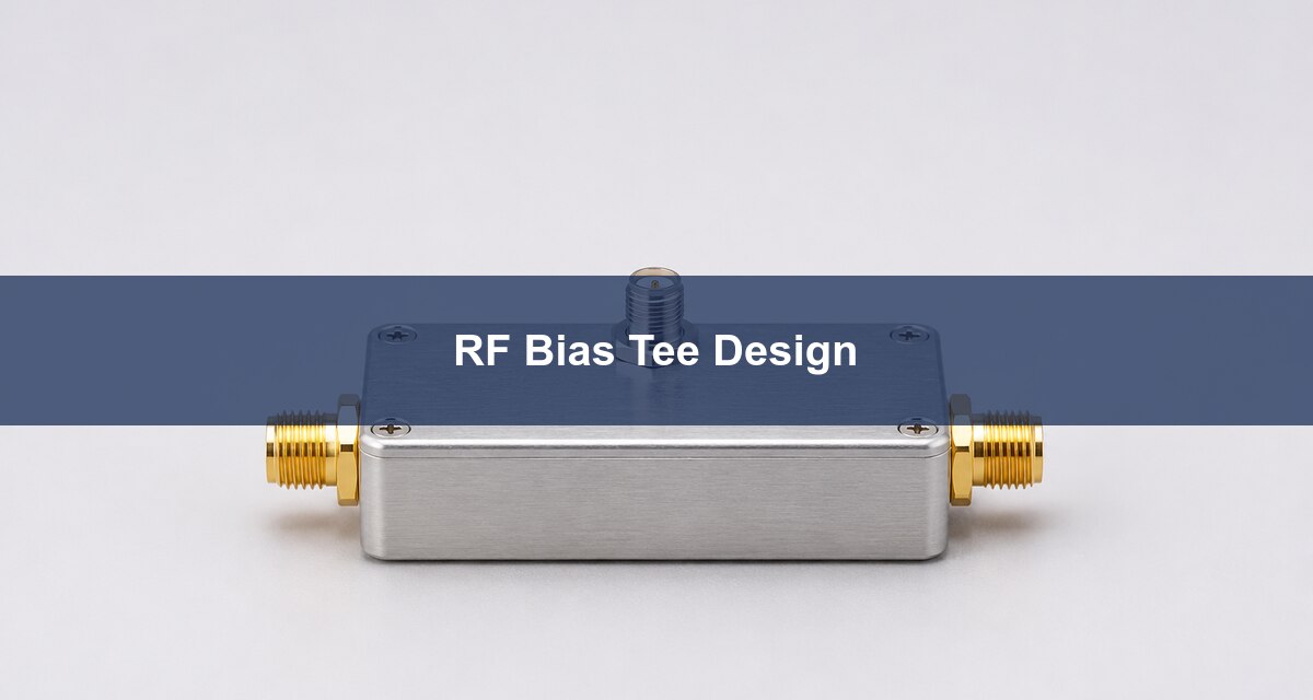
The RF-only port reaches the combined RF+DC node through a series DC-blocking capacitor. The DC port reaches that node through a choke or engineered high-impedance RF branch. At DC the capacitor blocks steady current and the choke carries the bias load. In the useful RF band the capacitor gives the signal an easy path, while the choke presents high impedance toward the supply. Use the connector labels or schematic rather than assuming ports are interchangeable.
RF Bias Tee Design: Set the Low-Frequency Edge First
For a hypothetical 50 Ω path starting at 100 MHz, a first screen might require capacitor reactance no greater than 5 Ω and choke reactance at least 500 Ω at that edge. The ideal relations give C ≥ 1/(2πf × 5 Ω) ≈ 318 pF and L ≥ 500 Ω/(2πf) ≈ 796 nH. The 5 Ω and 500 Ω figures are example design targets, not standards or guaranteed isolation. This screening assumes ideal parts and ignores the real supply and load impedances. Do not buy parts or approve attenuation from these two values alone.
DC Blocking Capacitor Selection: Check More Than Capacitance
Choose the capacitor using the actual voltage across it and the installed RF response. If the RF+DC side sits at a DC potential while the RF-only side is near ground, the capacitor can see nearly the full bias voltage, plus any signal or transient. Check the manufacturer’s voltage rating, effective capacitance, impedance versus frequency and mounting model. A part large enough at 100 MHz may be inductive or interact with the launch at the upper end. Characterize the same package and pads used in production.
RF Choke Inductor: Verify Isolation and DC Headroom
Choose the choke by impedance over the operating band and by its ability to carry the bias current. Check impedance under relevant bias where data are available, DCR at operating temperature and the applicable current limits. For example, an assumed 0.30 Ω bias path at 150 mA drops 45 mV and dissipates 6.75 mW. Include any other series path drops and verify the minimum voltage at the device.
Wideband Bias Tee Design: Single Choke vs Broadband Network
A single L and C are a useful starting point for a restricted band. For several octaves, the choke, capacitor and board can introduce resonances; a specialized broadband choke or staged network may be preferable. Analog Devices AN-2061 documents a specific wideband PCB implementation. Treat it as a method and a verified example for that device, not as a parts list for an arbitrary amplifier.
| Approach | Choose when | What may limit it |
| Single on-board choke | A defined band fits the verified part model. | Poor isolation near the low edge; resonance near the high edge. |
| Broadband or staged feed | Single parts cannot meet both ends of the band. | Part-to-part and layout interactions can add notches. |
| Connectorized bias tee | You need a known reference or a removable bench solution. | Extra connectors and cables add loss, space and calibration work. |
Bias Tee PCB Design: Keep the Junction Compact
Treat the junction as an RF discontinuity. Keep the side branch short before the choke, keep the RF reference plane continuous, and place RF-relevant bypassing on the supply side with a short return. Pads, ground vias and connector launches belong in the model. See the Best Technology microstrip layout guide for the controlled line and return path. Avoid leaving an unused path to a DC test pad at the RF junction without evaluating it as a stub.
Bias Tee Insertion Loss: Compare Against a Reference
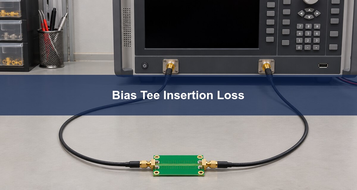
Measure RF transmission between the RF-only and combined ports using a DC-safe setup and a like-for-like reference line or calibrated reference planes. Keep connector launches and stackup comparable. Record return loss too: a notch with degraded matching suggests investigating the junction or resonance rather than attributing the loss to the laminate. Repeat at the expected bias and temperature conditions where the measurement setup supports it.
Bias Tee S Parameters: Specify the DC Port Condition
Record which physical port is used for each measurement and what terminates the third port. A supply, a bypassed feed and a 50 Ω calibration load are not equivalent. Measure leakage from the combined port toward the bias branch with a suitably protected receiver and the specified measurement termination. Independently verify the bias network under its actual supply and load. Before applying bias, verify every instrument’s port DC limits and protection, and follow the active device’s sequencing instructions. The Analog Devices ADL9005 evaluation-board guide gives one device-specific sequencing example.
| Acceptance check | Evidence | If it fails |
| RF transmission and match | Loss and reflection traces over the required band at stated reference planes. | Recheck transitions, series capacitor and resonance. |
| RF leakage to bias feed | Isolation trace with port IDs, termination and bias condition. | Check choke impedance and bypass return. |
| DC delivery | Voltage at the device under load and acceptable temperature rise. | Check DCR, current limits and upstream headroom. |
FAQ
Is a bias tee the same as a DC block?
No. A DC block supplies the series capacitor function; a bias tee also has a way to feed or extract DC at the shared node.
Can I use a larger choke to improve isolation everywhere?
No. A larger nominal inductance may have a different resonance and impedance curve. Compare the installed response across the band.
Can a ferrite bead replace the inductor?
Only if its impedance under bias and the resulting network meet your limits. Treat it as a different design to verify.
Why does the board work without bias but fail at operating current?
The choke response and DC voltage drop can change with current or temperature. Repeat the check at the real operating point.
Why does connecting the real supply change the RF trace?
Its impedance and wiring can change the termination seen through the bias branch. State that condition and compare it with the bench setup.
Can the combined port go directly into a network analyzer?
Only if the instrument and measurement hardware explicitly tolerate that DC condition. Verify limits and use appropriate DC protection before connecting.
When is an external bias tee useful?
Use a characterized external part for comparison when you want to separate the active device from a new PCB bias network.
How do I qualify a substitute choke?
Compare impedance, package and DC limits, then repeat transmission, isolation and loaded-voltage measurements on the production footprint.
Prepare the RF Stackup and Coupon Review
For a Best Technology PCB discussion, send the operating band, bias load, stackup, connector drawings and required isolation to sales@bestpcbs.com. Include which reference planes and terminations define the measurements.