An 868 MHz PCB antenna has a theoretical quarter-wave length of approximately 86.3 mm, but a compact printed antenna does not need an 86.3 mm straight trace. Its actual dimensions depend on the antenna structure, PCB ground plane, dielectric material, and installation environment.
For an 868 MHz LoRa sensor or industrial IoT device, the practical questions are which antenna fits the PCB, how much ground clearance it requires, and what to change when the measured resonance or communication range is wrong. Proven designs such as TI DN023 and TI DN024 provide useful starting geometries, but their performance must be verified on the actual product.

What Should You Consider Before Designing an 868 MHz PCB Antenna?
For an 868 MHz PCB antenna, start by defining the required frequency range, available PCB area, RF interface, and installation conditions. These four requirements determine whether a printed antenna is practical before any copper pattern is drawn.
- Operating frequency: Identify the actual channels. For example, European LoRaWAN devices may use 868.1, 868.3, and 868.5 MHz. The antenna must cover the required channels, not just a single nominal frequency.
- Available PCB area: Measure the space available for both the radiator and the ground plane. A 43 × 20 mm antenna region does not mean the entire antenna system occupies only that area.
- RF interface: Check whether the radio module provides a nominal 50-ohm antenna port. A bare RF transceiver may require additional output matching, filtering, or a balun.
- Performance requirements: Establish the operating bandwidth, acceptable S11 or VSWR, radiation performance, and wireless link requirements.
- Mechanical conditions: Confirm the location of the battery, enclosure, mounting hardware, and nearby metal before fixing the antenna position.
If the PCB cannot accommodate a suitable radiator and ground structure, a chip antenna or external antenna may be more practical. Reducing the size of a printed antenna without redesigning it can compromise radiation efficiency and bandwidth.
Which 868 MHz PCB Antenna Type Is Best for Your Device?
A meandered monopole or inverted-F antenna (IFA) is generally a practical starting point for a compact 868 MHz PCB. A straight monopole is simpler, but its physical length is difficult to accommodate in many small devices.
The choice depends on the available board geometry.
- Straight monopole: Consider this when sufficient conductor length and an appropriate ground structure are available. Its relatively simple shape can make development easier, but it is less convenient for compact products.
- Meandered monopole: Suitable when the radiator must fit into a smaller area. Folded traces reduce the physical footprint, although coupling between neighboring sections makes the antenna sensitive to dimensional changes.
- Inverted-F antenna: Suitable when the PCB can support a controlled ground structure and shorting connection. Feed position and radiator geometry provide a way to influence input impedance.
Two useful starting points are TI DN023, an inverted-F antenna, and TI DN024, a meandered monopole.
DN023 is worth evaluating when a compact radiator and its associated ground region can be accommodated. DN024 is attractive when a longer supporting ground plane is available and the layout can preserve its specified two-sided radiator geometry.
Neither design should be selected solely because its antenna pattern appears smaller. The required ground structure and clearance must also fit the product.
How Do You Calculate 868 MHz PCB Antenna Length and Dimensions?
At 868 MHz, the free-space wavelength is approximately 345.4 mm, giving a theoretical quarter-wave length of 86.3 mm.
That length is useful for understanding the electrical scale of the antenna. It is not a fixed fabrication dimension for a meandered monopole or inverted-F design. Folding conductors changes electromagnetic coupling, while the PCB ground plane and dielectric environment influence resonance.
The following reference dimensions provide a more useful starting point.
| Parameter | TI DN023 | TI DN024 |
|---|---|---|
| Antenna type | Inverted-F | Meandered monopole |
| Antenna region | 43 × 20 mm | 38 × 25 mm |
| Ground plane | 45 × 31 mm | 43 × 63 mm |
| FR4 thickness | 0.8 mm | 1.6 mm |
| Radiator trace width | 1.0 mm | 2.0 mm |
| Main tuning feature | L6 radiator segment | L4 end segment and matching |
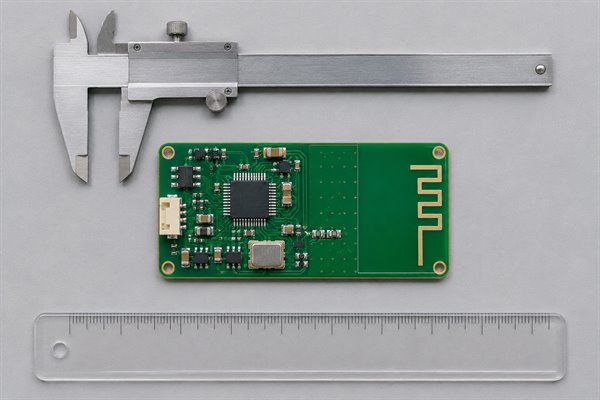
These dimensions must be interpreted with the reference layouts. The antenna region and ground plane are separate parts of the overall PCB geometry.
For TI DN023, the dimension drawing identifies an initial L6 length of 17 mm. With the specified 31 × 45 mm ground plane, the recommended L6 length is approximately 9 mm for 868 MHz.
L6 is the right-hand end segment of the printed radiator, not the entire antenna length. Changing its length alters the electrical behavior of the antenna and is one of the ways the reference design can be adjusted for different frequencies.
For TI DN024, the radiator occupies approximately 38 × 25 mm, with a 43 × 63 mm ground region. Its layout includes an L4 end segment, and the reference documentation distinguishes the geometry used for single-band and dual-band configurations.
A larger ground plane or different enclosure can change the required tuning, so copying the radiator alone is insufficient.
For a new design, select the reference geometry that fits the available board area, import the original antenna copper pattern where possible, and preserve its supporting ground structure. If the dimensions must change, verify the modified geometry through simulation or prototype measurements instead of scaling the pattern uniformly.
Which PCB Materials and Stackups Work Best for 868 MHz Antennas?
Two-layer FR4 is the most practical starting point for many conventional 868 MHz PCB antennas. The appropriate board thickness depends on the selected reference design. Four-layer FR4 is also possible, while low-loss RF laminates should be considered when their electrical advantages justify redesigning the antenna.
The following choices provide a useful engineering starting point:
- 0.8 mm FR4 based on TI DN023: Appropriate when using the DN023 inverted-F geometry. Its antenna region has no underlying ground plane. Changing substrate thickness may require adjustment of the radiator length.
- 1.6 mm FR4 based on TI DN024: Appropriate for the DN024 meandered monopole. This reference uses antenna copper patterns on both the top and bottom layers, with no ground plane beneath the radiator. Changing thickness may require a different matching network.
- Four-layer FR4: Suitable when the wireless device needs additional routing, power distribution, or internal reference planes. The antenna keep-out must be preserved on the relevant layers, and the RF feed must be recalculated for the actual stackup.
- Low-loss RF laminate: Consider this when measured dielectric loss or efficiency requirements cannot be satisfied with the chosen FR4 construction. A different dielectric constant or thickness changes the electromagnetic design and requires verification.
For a typical 868 MHz sensor using DN023 or DN024, start with the specified FR4 construction rather than substituting an expensive RF laminate. The reference geometry and its measured performance provide a stronger basis for material selection than frequency alone.
The principal material parameters are dielectric constant (Dk), dissipation factor (Df), substrate thickness, and finished copper dimensions. These affect RF feed impedance, conductor loss, and the loading of the radiator.
For example, transferring a two-layer DN024 antenna to a four-layer PCB is not simply a matter of adding two copper layers. If an internal ground plane extends beneath the antenna region, it changes the electromagnetic environment. That adaptation should be treated as a revised antenna design rather than an unchanged reference implementation.
How Should You Design an 868 MHz PCB Antenna Layout and Ground Plane?
Place the radiator at a suitable PCB edge, preserve the required ground geometry, and keep prohibited copper and components outside the antenna region. These are the main layout requirements for a printed 868 MHz antenna.
Consider a hypothetical 55 × 75 mm PCB intended for an 868 MHz sensor. You want to evaluate whether the TI DN023 reference geometry can fit.
The DN023 radiator is 43 mm wide and 20 mm deep, while its supporting reference ground region is 45 × 31 mm. Placing the antenna along the 55 mm board edge leaves approximately 6 mm on each side of the 43 mm radiator.
This allows an initial geometric check against DN023’s minimum 5 mm lateral clearance recommendation for nearby ground copper and components when the board is wider than the reference antenna. The radiator and reference ground extend roughly 51 mm along the board length, leaving approximately 24 mm of the 75 mm board length for any additional layout area.
However, those dimensions alone do not establish a valid design. The actual ground outline, RF feed, remaining circuitry, battery, and enclosure still have to be checked. The example is a space-allocation exercise, not a verified antenna layout.
For the final PCB, apply these rules:
- Keep the radiator geometry unchanged initially. Preserve its trace width, spacing, feed point, and shorting structure.
- Maintain the reference ground plane. Do not assume that increasing or reshaping the ground area will improve antenna performance.
- Clear prohibited copper on all affected layers. Do not route signals, add vias, or extend inner ground planes beneath antenna regions that require clearance.
- Keep the RF feed controlled. Maintain the intended transmission-line impedance between the radio interface, matching network, and antenna feed.
- Protect the antenna region from nearby conductors. Avoid placing large metal components or unintended copper features close to the radiator.
The 5 mm clearance is specific to the DN023 implementation described above. It is not a universal 868 MHz antenna design rule.
A useful final layout review compares the new board against the complete reference artwork, including the radiator, feed, ground plane, and clearance boundaries. Differences in these features matter more than visual similarity between antenna traces.
How Do You Design the RF Feed Line and Match an 868 MHz PCB Antenna to 50 Ohms?
Use a controlled-impedance RF feed, normally 50 ohms, and match the measured antenna input impedance to the radio interface. The antenna’s physical geometry determines its input impedance; a 50-ohm transmission line does not automatically create a 50-ohm antenna.
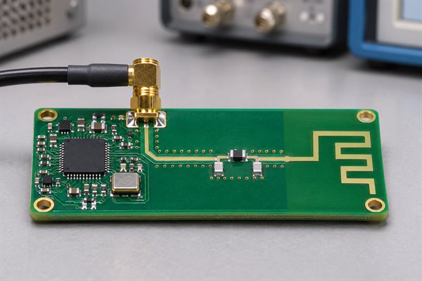
The feed may use microstrip or grounded coplanar waveguide geometry, calculated from the actual laminate thickness, dielectric properties, copper dimensions, and reference ground arrangement.
A matching network near the feed point allows the measured antenna impedance to be transformed toward the system’s target value.
The difference between TI DN023 and DN024 illustrates two practical situations.
TI DN023: Its antenna impedance is approximately matched to 50 ohms in the reference configuration, so external antenna matching components are not necessarily required. The layout still provides optional matching positions to compensate for changes caused by the ground plane or enclosure.
TI DN024: Its documented 868 MHz single-band matching configuration uses a 1.8 nH series inductor and a 2.7 pF shunt capacitor. The measured standing-wave ratio improved to approximately 1.1:1 in that specific reference design.
For a custom board, determine the values from measured impedance rather than copying the reference BOM.
A practical matching sequence is to measure the antenna input with a calibrated VNA, inspect its complex impedance on a Smith chart, select a suitable series/shunt network, and remeasure the complete operating band.
S11 of -10 dB or lower is a common initial matching target for many 50-ohm systems, corresponding to approximately 10% reflected power. The exact requirement depends on the required channels and system performance.
Matching can reduce reflected power, but it cannot automatically correct poor radiation efficiency or an unsuitable mechanical antenna location.
How Do Enclosures, Batteries, and Nearby Metal Affect 868 MHz PCB Antenna Performance?
Nearby conductive objects and dielectric materials can shift resonance and reduce radiation efficiency after assembly. The antenna should therefore be tuned in the mechanical configuration in which the device will operate.
The effects differ by material. Metal brackets and enclosures may redirect or shield radiation. Battery casings introduce large conductive surfaces, while plastic housings add dielectric loading. Displays and conductive coatings can also alter the field around the radiator.
A useful experiment is to measure the same prototype in three conditions: bare PCB, PCB with battery installed, and fully assembled device.
Suppose the bare PCB has its lowest S11 near 868 MHz, but the response shifts downward after the battery is fitted. Compare the battery position, clearance, and any newly introduced conductive structures. If moving the battery away from the radiator restores the response, the mechanical arrangement is a likely contributor.
The next action is not necessarily to change matching components. Increasing separation or moving the radiator may preserve efficiency more effectively than matching an antenna in an unfavorable location.
For equipment mounted against metal machinery or installed inside a cabinet, also evaluate performance in the intended mounting position. A design tuned in free space may not reproduce the same behavior after installation.
How Do You Test and Tune an 868 MHz PCB Antenna?
Measure S11 and input impedance first, then verify the antenna’s radiated performance in the finished device. A low reflection coefficient indicates good input matching; it does not establish radiation efficiency.
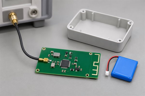
Use the following sequence.
Step 1: Measure the antenna input.
Calibrate a vector network analyzer (VNA) at the appropriate reference plane. An initial sweep of approximately 800–930 MHz can locate the main response around 868 MHz. Then measure the actual operating channels more closely.
Keep the test cable from coupling excessively to the radiator, as the cable can alter the measured response.
Step 2: Check the matching response.
At a nominal 50-ohm interface, S11 of -10 dB means approximately 10% of incident power is reflected. A value of -15 dB corresponds to about 3.2% reflection.
Check the input impedance and the bandwidth over which the required matching criterion is met. Do not judge the antenna solely by the deepest point of the S11 curve.
Step 3: Decide whether geometry or matching requires adjustment.
If the antenna’s natural resonant behavior is outside the required frequency range, inspect the radiator and ground geometry. If resonance is suitable but the input impedance is poorly matched, adjust the matching network.
For a useful reference, TI DN024 achieved approximately 88 MHz of matched bandwidth, from 825 to 913 MHz, at its 2:1 VSWR criterion in the documented 868 MHz single-band configuration. This is reference-design performance, not a universal requirement.
Step 4: Verify the final device.
Repeat the measurements with the battery and enclosure installed. Then assess actual wireless performance under consistent transmit power, radio settings, orientation, and environmental conditions.
Record RSSI, SNR, and packet delivery performance. If the specification requires radiation efficiency, realized gain, or radiation patterns, use suitable over-the-air test equipment.
Why Is Your 868 MHz PCB Antenna Losing Range or Shifting Resonance?
Start with the measured symptom rather than changing antenna dimensions immediately. A resonance shift, poor impedance match, and weak wireless link can have different causes.
The following examples illustrate how to interpret the measurements. The numerical scenarios are hypothetical troubleshooting cases, not reported results from a manufactured prototype.
| Measured Symptom | Likely Area to Investigate | First Action |
|---|---|---|
| S11 minimum near 830 MHz instead of the intended 868 MHz | Radiator electrical length, ground geometry, dielectric loading, or matching effects | Compare the copper pattern and ground structure with the reference; inspect the unmatched impedance response |
| S11 near -5 dB at 868 MHz | Input impedance mismatch | Check the measurement reference plane, feed, and matching network; inspect the Smith chart |
| S11 near -18 dB at 868 MHz but communication range remains poor | Radiation efficiency, antenna orientation, radio settings, or interference | Check the RF link budget and radiated performance rather than continuing to optimize S11 |
| Performance deteriorates after enclosure assembly | Battery, metal, or dielectric loading | Compare bare-board and assembled-device measurements |
| Different prototypes give different results | Fabrication, component, or assembly variations | Compare finished antenna geometry, stackup, BOM, and test setup |
A low-frequency S11 minimum does not always mean the radiator is simply too long, because matching components can also influence the reflection curve. Confirm the antenna’s impedance behavior before shortening a trace.
For LoRa devices, communication range also depends on spreading factor, bandwidth, output power, receiver sensitivity, interference, and propagation conditions.
A useful diagnostic separation is:
- Resonance or matching problem: Investigate antenna geometry, RF feed, grounding, and matching.
- Good matching but poor wireless range: Investigate radiation efficiency, installation, polarization, and link-budget conditions.
- Different results after production: Investigate changes in material, copper geometry, components, and assembly.
This prevents unnecessary PCB redesign when the problem originates elsewhere in the RF system.
FAQs About 868 MHz PCB Antennas
Q1: Can the Same 868 MHz PCB Antenna Support LoRa, FSK, and Wireless M-Bus?
A1: Yes. An 868 MHz PCB antenna can support LoRa, FSK, and Wireless M-Bus when their frequency and bandwidth requirements are compatible. The modulation and protocol are determined by the radio, not the antenna.
Q2: Can One PCB Antenna Operate at Both 868 MHz and 915 MHz?
A2: Yes, if matching and radiation performance are adequate at both frequencies. A narrowband antenna tuned for 868 MHz may not perform well at 915 MHz. Both operating bands must be verified.
Q3: Can an 868 MHz PCB Antenna Be Used in the United States?
A3: Not automatically. Many US unlicensed sub-GHz IoT devices operate in the 902–928 MHz band, while 868 MHz is commonly associated with European short-range systems. Check the applicable FCC requirements and authorized operating frequencies.
Q4: Can an 868 MHz PCB Antenna Be Used for UHF RFID?
A4: Yes, with a design appropriate for the RFID application. European UHF RFID uses frequencies around 865–868 MHz. Passive RFID tag antennas must match the chip’s complex impedance, which differs from a typical 50-ohm radio interface.
Q5: Do 868 MHz Devices Require Separate Transmit and Receive Antennas?
A5: No. Many 868 MHz transceivers use one shared antenna for transmitting and receiving. Separate antennas are used when a particular system requires diversity, additional isolation, or specialized simultaneous operation.
Q6: Is an 868 MHz PCB Antenna Omnidirectional?
A6: Some printed monopoles provide approximately omnidirectional coverage in certain planes, but no practical antenna radiates equally in every direction. The ground plane and antenna geometry influence the radiation pattern and its nulls.
Q7: What Does -2 dBi Antenna Gain Mean?
A7: A value of -2 dBi means the specified gain is 2 dB below an ideal isotropic radiator in the stated direction. Distinguish antenna gain from realized gain, which includes the effect of impedance mismatch.
Q8: Does an 868 MHz PCB Antenna Require ESD Protection?
A8: ESD protection depends on the product and its exposure conditions. Accessible antenna connections may require protection. RF protection devices should have low parasitic capacitance and insertion loss to minimize unwanted loading.
Q9: Can 868 MHz and 2.4 GHz Share One PCB Antenna?
A9: Yes, with a purpose-designed multiband antenna and suitable RF circuitry. TI DN024 includes a separate dual-band configuration for 868 MHz and 2.44 GHz. Its single-band matching configuration is not suitable for both frequencies unchanged.
Q10: What Manufacturing Data Should Accompany an 868 MHz PCB Antenna RFQ?
A10: Send Gerber or ODB++, the stackup, impedance notes, BOM, quantities, and approved antenna and keep-out drawings. If assembly or tuning support is required, also provide component tolerances, enclosure conditions, and measurable test acceptance criteria.
Conclusion
An 868 MHz PCB antenna should be selected using its complete reference geometry, including the supporting ground plane and available clearance. For compact IoT hardware, start with a verified design, preserve the critical copper pattern, and use measured impedance and wireless performance to guide changes.
Need a custom 868 MHz PCB antenna board manufactured for your device? EBest Circuit supports PCB fabrication and assembly from customer-approved designs, including prototypes and production projects.
Send your Gerber files, PCB stackup, BOM if assembly is required, quantity, target delivery date, and delivery location to sales@bestpcbs.com for a free DFM check and quotation.