PCB manufacturing PCB manufacturing
Home > Blog

What Is Isola IS400? Mid-Tg Lead-Free Epoxy Laminate & Prepreg

July 6th, 2026

Isola IS400 is a mid-Tg, lead-free epoxy laminate and prepreg material for reliable multilayer PCB manufacturing. It is used when a PCB needs better thermal stability than basic FR4 while keeping normal FR-4 process compatibility.

This guide explains Isola IS400 material properties, datasheet values, Tg rating, Dk, Df, thermal conductivity, lead-free PCB use, applications, FR4 comparison, 370HR comparison, alternative material models and selection checks.

Isola IS400, https://www.bestpcbs.com/blog/2026/07/isola-is400/

What Is Isola IS400?

Isola IS400 is a lead-free, mid-Tg epoxy laminate and prepreg system for multilayer PCB fabrication. It is built for PCB projects that need stronger heat resistance than many standard FR4 materials but do not require premium RF or microwave laminates.

The material uses an epoxy resin system reinforced with electrical-grade E-glass fabric. This structure gives the PCB mechanical strength, dielectric insulation and thermal stability during fabrication and lead-free assembly.

In PCB production, Isola IS400 is valued for balanced performance. The laminate works as the rigid copper-clad core, while the prepreg bonds layers during multilayer lamination. Together, they support stable stackup construction and practical cost control.

Why Is Isola IS400 Used for Lead-Free PCB Manufacturing?

Isola IS400 is used for lead-free PCB manufacturing because it offers better thermal stability than many basic FR4 materials. Lead-free soldering usually requires higher peak temperatures, which can stress the laminate, prepreg and plated through holes.

During lead-free reflow, the PCB must resist delamination, blistering, excessive expansion and resin breakdown. The Tg 150°C and Td 330°C values help the board tolerate these conditions more reliably.

The material is also FR-4 process compatible. A capable PCB factory can process it through controlled storage, lamination, drilling, desmear, plating, baking and final inspection.

For many multilayer PCB projects, Isola IS400 is a practical choice when the design needs lead-free reliability without moving to a costly specialty laminate.

Isola IS400 Material Properties and Datasheet Overview

Isola IS400 material properties include Tg 150°C, Td 330°C, Dk 3.90, Df 0.022 and thermal conductivity 0.36 W/m·K. These Isola IS400 technical specifications define thermal behavior, electrical performance, lead-free assembly resistance and multilayer PCB process stability.

PropertyValueUnit
Tg150°C
Td330°C
Dk3.90—
Df0.022—
Thermal Conductivity0.36W/mĀ·K
Z-Axis CTE Before Tg50ppm/°C
Z-Axis CTE After Tg250ppm/°C
T260>60min
T288>10min
Laminate Thickness0.05–2.4mm
Copper Weight18–70µm
ComplianceRoHS—
UL FileE41625—
IPC Reference4101 /97 /98 /99 /101—

The Isola IS400 datasheet shows that this material is not an ultra-low-loss laminate. Instead, it is a mid-Tg lead-free material for PCB projects that need stable thermal performance, defined dielectric values and reliable multilayer processing.

What Is the Tg Rating of Isola IS400?

The Tg rating of Isola IS400 is 150°C. Tg means glass transition temperature, which is the temperature range where the resin system changes from a rigid state to a softer state.

This value matters because PCB materials expand faster after reaching Tg. If the laminate has a low Tg, lead-free reflow and thermal cycling can increase the risk of delamination, hole wall stress, warpage and long-term failure.

An Isola IS400 Tg 150 material is usually stronger than many standard FR4 choices for lead-free PCB assembly. However, for harsh thermal cycling, thick copper, high layer counts or stricter reliability requirements, a high-Tg material such as Isola 370HR may be more suitable.

What Are the Dk, Df and Thermal Conductivity of Isola IS400?

The typical Dk is 3.90, the Df is 0.022 and the thermal conductivity is 0.36 W/mĀ·K. These values affect signal behavior, dielectric loss and heat transfer in PCB design.

Dk, or dielectric constant, affects signal speed and controlled impedance. A Dk of 3.90 is suitable for many digital, industrial and control PCB designs, but final impedance still depends on dielectric thickness, copper thickness, resin content and glass style.

Df, or dissipation factor, affects signal loss. A Df of 0.022 is acceptable for general multilayer PCB designs, but it is not ideal for RF, microwave or very high-speed low-loss applications.
Isola IS400 thermal conductivity is typical for glass-reinforced epoxy material. Heat still needs to be managed with copper planes, thermal vias, balanced stackup design and proper component placement.

What Applications Commonly Use Isola IS400 PCB Material?

Isola IS400 PCB material is commonly used in products that need mid-level thermal reliability, multilayer stability and lead-free soldering compatibility. It fits reliability-focused PCB projects across industrial and commercial electronics.

Common applications include:

  • Industrial control systems: PLC boards, automation control PCB and machine electronics.
  • Automotive electronics: control modules, sensor support boards and power management PCB.
  • Power supply electronics: control boards, converter support circuits and driver PCB.
  • Commercial multilayer PCB: general electronics needing better heat resistance than basic FR4.
  • LED control boards: driver control circuits and lighting-related electronics.
  • Instrumentation PCB: monitoring, testing and measurement equipment.
  • Communication support boards: non-RF multilayer PCB with stable dielectric requirements.
  • Consumer and office electronics: reliable PCB designs using lead-free assembly.

For high-speed backplanes, RF circuits, microwave systems or ultra-low-loss signal paths, a lower-Df material should be reviewed before choosing this laminate.

Isola IS400 vs FR4: What Is the Difference?

Isola IS400 is a defined mid-Tg lead-free material, while FR4 is a broad material category with many grades. Standard FR4 may have lower Tg, weaker thermal resistance or less predictable datasheet values.

ItemIsola IS400Standard FR4
Material TypeMid-Tg epoxy laminate and prepregGeneral glass-reinforced epoxy category
Tg150°COften 130–140°C, varies by grade
Td330°CVaries by resin system
Dk3.90Usually around 4.0, varies by supplier
Df0.022Varies by grade and test frequency
Thermal Conductivity0.36 W/mĀ·KUsually similar range, varies by material
Lead-Free AssemblyBetter fit than many low-Tg FR4 choicesDepends on Tg, Td and PCB thickness
Multilayer ReliabilityMore stable for demanding lead-free PCB useSuitable for simple and standard multilayer PCB
Z-Axis ExpansionDefined CTE dataDepends on laminate grade
CAF ResistanceDesigned for reliability-focused PCB useDepends on material grade
Process CompatibilityFR-4 compatibleStandard FR4 process
Cost LevelHigher than basic FR4Lower in simple PCB projects
Best UseReliable multilayer PCB, industrial PCB, lead-free PCBLow-cost general PCB

Choose Isola IS400 when the PCB needs better lead-free reflow performance, defined material data and improved multilayer reliability. Choose standard FR4 when the design is simple, low-cost and not exposed to demanding thermal conditions.

Isola IS400 vs FR4, https://www.bestpcbs.com/blog/2026/07/isola-is400/

Isola IS400 vs 370HR: Which Material Should You Choose?

Choose Isola IS400 for balanced mid-Tg performance and choose 370HR for higher thermal reliability. Both materials are used in multilayer PCB fabrication, but they serve different reliability levels.

ItemIsola IS400Isola 370HR
Material ClassMid-Tg lead-free epoxy laminateHigh-Tg FR-4 multifunctional epoxy laminate
Tg150°C180°C
Td330°C340°C
Dk3.904.04
Df0.0220.021
Thermal Conductivity0.36 W/mĀ·K0.4 W/mĀ·K
Z-Axis CTE Before Tg50 ppm/°C45 ppm/°C
Z-Axis CTE After Tg250 ppm/°C230 ppm/°C
T260>60 min60 min
T288>10 min30 min
HDI SuitabilitySuitable for standard multilayer PCBBetter fit for HDI and sequential lamination
Thermal CyclingGood for mid-level reliabilityBetter for harsher reliability demands
Cost LevelUsually lowerUsually higher
Best UseIndustrial, commercial and lead-free multilayer PCBHigh-reliability, high-layer-count and thermally demanding PCB

Isola IS400 is a practical choice for industrial control, commercial electronics and mid-level lead-free applications. 370HR is better when the PCB faces higher thermal cycling, thicker copper, higher layer count, multiple reflow cycles or stricter long-term reliability requirements.

Isola IS400 vs 370HR, https://www.bestpcbs.com/blog/2026/07/isola-is400/

What Are the Alternative Materials to Isola IS400?

Alternative materials to Isola IS400 include specific mid-Tg, high-Tg and lower-loss laminate models. The right replacement depends on Tg, Df, lead-free assembly requirements, availability, cost target and PCB reliability level.

Material ModelSupplierMaterial TypeBest Fit
Isola 370HRIsolaHigh-Tg FR-4 laminate and prepregHigher thermal reliability and high-layer-count PCB
Isola IS410IsolaHigh-Tg FR-4 epoxy laminate and prepregMultiple thermal excursions and reliable multilayer PCB
Isola FR408HRIsolaMid-loss FR-4 laminate and prepregLower-loss digital PCB and higher-speed signal designs
Isola FR406IsolaFR-4 epoxy laminate and prepregGeneral multilayer PCB where IS400 is not required
Shengyi S1000-2MShengyiHigh-Tg lead-free FR-4 laminateHigh-layer-count PCB and automotive electronics
Shengyi S1000-2ShengyiHigh-Tg FR-4 laminate systemIndustrial multilayer PCB and lead-free PCB production
ITEQ IT-180AITEQHigh-Tg low-CTE laminate and prepregHigh-layer PCB, lead-free assembly and CAF resistance
Panasonic R-1755VPanasonicHigh-Tg FR-4 laminateLead-free multilayer PCB with stable thermal reliability
Panasonic MEGTRON 6PanasonicLow-loss laminateHigh-speed PCB where signal loss is more important
Rogers RO4350BRogersHydrocarbon ceramic laminateRF PCB, microwave PCB and antenna PCB

Use Isola 370HR, IS410, S1000-2M or IT-180A when the design needs higher Tg and stronger thermal reliability. Use FR408HR or MEGTRON 6 when lower signal loss matters. Use Rogers RO4350B only when RF or microwave performance is the main requirement.

What Should You Check Before Choosing Isola IS400?

Before choosing Isola IS400, review the PCB design, assembly process, reliability target and supplier control ability. The material performs well only when it matches the actual stackup, operating environment and manufacturing process.

  • Confirm the real operating temperature.
    Check ambient temperature, component heat, enclosure temperature and thermal cycling. A Tg 150 material is suitable for many lead-free PCB projects, but higher-temperature environments may need a high-Tg laminate.
  • Review the reflow profile.
    Confirm peak temperature, time above liquidus and the number of reflow cycles. Thick PCB, heavy copper PCB and double-sided assembly create more thermal stress.
  • Check layer count and stackup balance.
    Higher layer counts require better registration, resin flow and lamination control. Unbalanced copper distribution can increase warpage risk.
  • Match copper weight with resin flow.
    Heavy copper affects etching, spacing, prepreg filling and press cycle design. The factory should confirm whether the selected prepreg can fill copper areas without voids.
  • Verify impedance requirements.
    Dk should be checked with the actual dielectric thickness, copper thickness and glass style. Controlled impedance PCB should not rely only on a catalog Dk value.
  • Evaluate humidity and voltage spacing.
    Humid environments, narrow spacing and higher voltage can increase insulation risk. CAF resistance, cleanliness and spacing rules should be reviewed for reliability-focused designs.
  • Select the right surface finish.
    ENIG, OSP, immersion silver and lead-free HASL can all be considered. The choice should match solderability, storage time, fine-pitch assembly, cost and inspection needs.
  • Confirm material traceability.
    Ask the PCB factory to confirm material grade, laminate batch, prepreg type and stackup before production. This prevents unapproved material replacement.
  • Define inspection requirements.
    For critical PCB orders, request electrical test, microsection, solderability check, impedance report and thermal stress review when needed.
  • Check production availability.
    Material availability can affect lead time and cost. Confirm stock status before urgent PCB fabrication or batch production.
Isola IS400 Selection Checklist, https://www.bestpcbs.com/blog/2026/07/isola-is400/

FAQs About Isola IS400 PCB Material

Q1: Why do some users search for ā€œis400 isolaā€?
A1: ā€œis400 isolaā€ usually means the same material as Isola IS400. Some users type the material code before the brand name. In PCB fabrication notes, write the full material name clearly to avoid confusion with generic FR4 or unapproved substitutes.

Q2: How should Isola IS400 be listed in PCB fabrication notes?
A2: Use a clear note such as: ā€œBase material: Isola IS400 laminate and prepreg, RoHS compliant, lead-free compatible.ā€ For controlled projects, also include finished thickness, copper weight, layer count, surface finish, impedance requirements and IPC class.

Q3: Can Isola IS400 be used for controlled impedance PCB?
A3: Yes. Controlled impedance is possible when the stackup uses the correct dielectric thickness, copper thickness and glass style. The typical Dk is 3.90, but final impedance should be confirmed by the PCB manufacturer before production.

Q4: Does Isola IS400 PCB need baking before assembly?
A4: Baking depends on storage time, packaging, humidity exposure and PCB thickness. If boards are exposed to moisture or stored for a long time, baking helps reduce blistering, delamination and soldering defects during lead-free reflow.

Q5: What copper weights are commonly used with Isola IS400?
A5: Common copper weights are 18 µm, 35 µm and 70 µm, equal to about 1/2 oz, 1 oz and 2 oz. Heavy copper designs need extra review because resin flow, spacing and lamination pressure become more difficult.

Q6: Can Isola IS400 support HDI PCB?
A6: It can support some dense multilayer PCB designs, but it is not the first choice for complex HDI. Multiple microvia layers, sequential lamination and tight reliability targets may require 370HR, IS410 or another higher-reliability material.

Q7: How should Isola IS400 prepreg be stored?
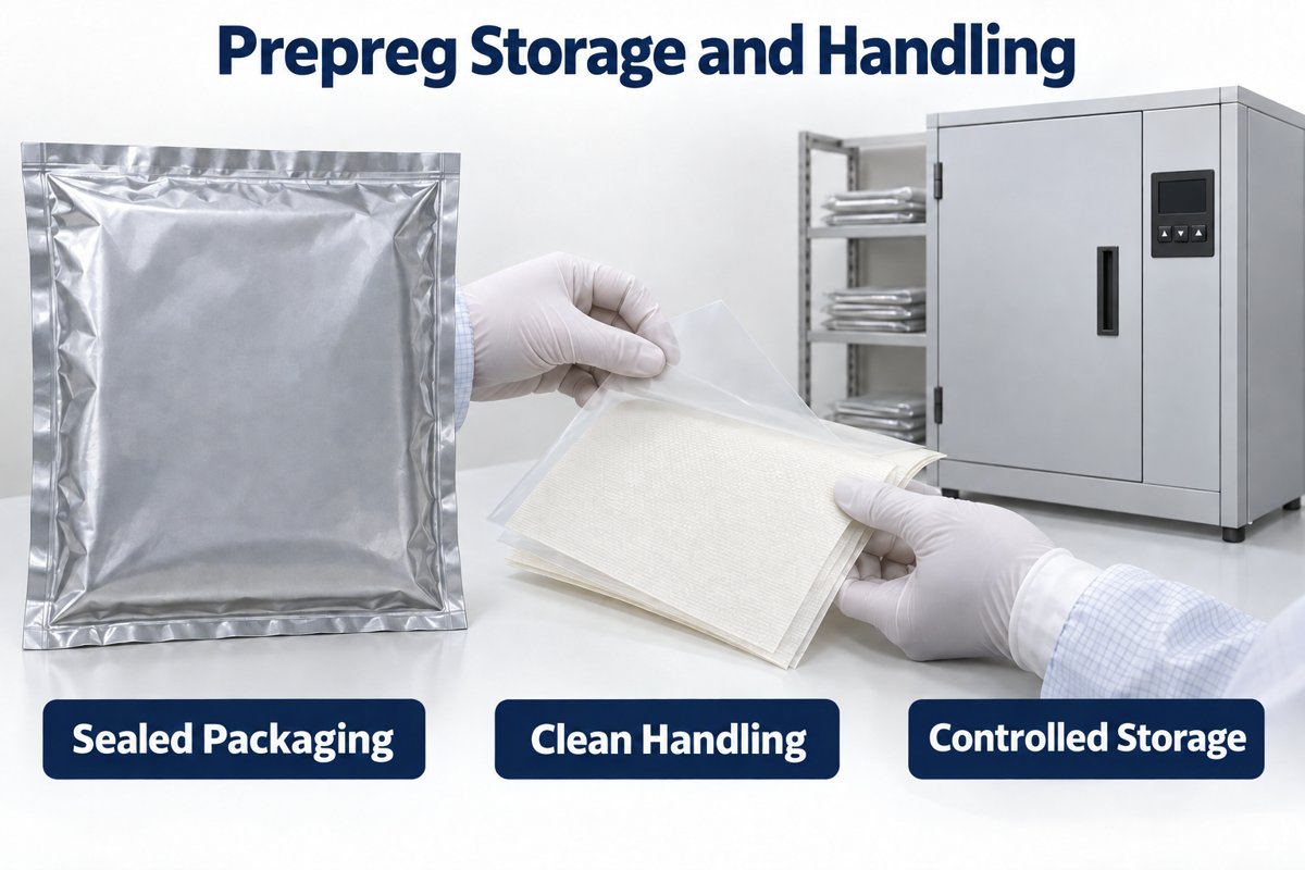
A7: Store prepreg in a clean, dry and temperature-controlled area. After opening, reseal unused prepreg quickly. Moisture exposure can reduce resin flow quality and increase voids, weak bonding or lamination defects.

Q8: What failures can happen if the wrong PCB material is used?
A8: Common risks include delamination, blistering, warpage, hole wall cracks, insulation failure and unstable impedance. These failures are more likely under lead-free reflow, high humidity, thermal cycling or heavy copper stress.

Q9: Can Isola IS400 replace Rogers materials?
A9: Usually no. Rogers materials are used for RF, microwave and low-loss circuits. Isola IS400 is mainly used for reliable multilayer PCB fabrication. It can replace basic FR4 in some thermal projects, but not RF laminates.

Q10: What does RoHS compliance mean for buyers?
A10: RoHS compliance means the material meets restricted-substance requirements for many electronics markets. Buyers should still request material certificates, compliance documents and production records before mass production.

Q11: Which surface finishes work with Isola IS400 PCB?
A11: Common finishes include ENIG, OSP, immersion silver and lead-free HASL. ENIG suits fine-pitch SMT and better pad flatness. OSP suits cost-sensitive PCB projects with shorter storage time.

Q12: What files are needed for an Isola IS400 PCB quote?
A12: Send Gerber files, drill files, stackup, finished thickness, copper weight, surface finish, solder mask color, impedance requirements, IPC class, quantity and testing requirements. For PCBA, also send BOM and Pick and Place files.

Q13: Can Isola IS400 be used for thick copper PCB?
A13: Yes, but the PCB stackup must be reviewed carefully. Thick copper increases resin filling demand, etching difficulty, spacing limits and thermal stress. The manufacturer should confirm prepreg selection, copper balance and lamination control.

Q14: How can buyers avoid material substitution?
A14: Ask for material brand, grade, laminate certificate, stackup confirmation and production records. For critical PCB orders, do not allow material changes without written approval. This helps prevent generic FR4 from replacing the specified material.

Isola IS400 is a practical mid-Tg lead-free laminate and prepreg material for multilayer PCB projects that need better thermal reliability than standard FR4 without moving to a premium low-loss material. Its main technical points are Tg 150°C, Td 330°C, Dk 3.90, Df 0.022 and thermal conductivity 0.36 W/m·K.

For material selection, match the laminate with stackup, copper weight, reflow profile, impedance control, operating environment and inspection requirements. If your PCB project needs stable lead-free assembly, controlled production, reliable material traceability and global delivery, EBest Circuit can support custom PCB fabrication from prototype to batch production. Send your Gerber files, stackup and project requirements to sales@bestpcbs.com for a fast Isola IS400 PCB quotation.

How to Identify Positive and Negative of Diode?

July 6th, 2026

Positive and negative of diode describes the two polarity terminals of a diode: the anode and the cathode, which decide how current should pass through the component. This article explains how to identify diode polarity by checking the body marking, symbol, terminal direction, band marking, multimeter reading, Zener diode polarity, LED diode legs, and PCB Assembly orientation.

For many users, the hard part is not knowing that a diode has polarity. The real problem is checking the right side on a real component before it is soldered, tested, or assembled onto a PCB.

Are you facing these problems when checking the positive and negative of a diode?

  • The diode has a band, but you are not sure whether it means positive or negative.
  • The schematic symbol is clear, but the real diode package looks different.
  • SMD diode markings are too small to read quickly.
  • LED diode legs have been cut, so the long-leg clue is gone.
  • A reversed diode may cause the PCBA to fail testing.

As a PCBA manufacturer, we reduce these risks by checking diode polarity from design review to final inspection.

  • We confirm the anode and cathode before SMT assembly.
  • We compare the schematic, BOM, footprint, and datasheet.
  • We verify the diode band, SMD mark, and PCB silkscreen.
  • We inspect LED polarity before and after soldering.
  • We use AOI, visual inspection, and functional testing to catch wrong orientation.

EBest Circuit (Best Technology) is a professional PCB and PCBA manufacturer offering PCB fabrication, component sourcing, SMT assembly, through-hole assembly, inspection, and functional testing. For diode-related PCB Assembly, we help customers confirm polarized components, reduce orientation mistakes, and improve first-pass yield from prototype to production. For PCB or PCBA projects, pls feel free to contact us at sales@bestpcbs.com.

positive and negative of diode

What Are the Positive and Negative of Diode?

The positive and negative of diode usually refer to its anode and cathode. In practical identification, the anode is commonly treated as the positive side, and the cathode is commonly treated as the negative side when the diode is forward-biased.

A diode is a directional component. It allows current to pass mainly in one direction and blocks current in the opposite direction. This is why diode polarity matters in power circuits, signal circuits, LED circuits, rectifier circuits, and PCB Assembly.

Diode PartCommon PolarityPractical Meaning
AnodePositive sideCurrent enters in forward bias
CathodeNegative sideUsually marked by a band
Band markingCathode sideShows the negative end in most common diodes
Forward biasAnode higher than cathodeDiode conducts
Reverse biasCathode higher than anodeDiode blocks current

The simple rule is this: anode = positive side, cathode = negative side in normal diode polarity identification. However, in real circuits, voltage conditions can vary, especially in Zener diode applications. That is why it is safer to identify the anode and cathode rather than only saying ā€œleft sideā€ or ā€œright side.ā€

In short, identifying the positive and negative of diode starts with understanding anode and cathode.

positive and negative of diode

Positive and Negative of a Diode: What Do Anode and Cathode Mean?

The positive and negative of a diode are more accurately described as anode and cathode. These two terms are used in schematics, datasheets, PCB footprints, assembly drawings, and inspection documents.

The anode is the terminal where conventional current enters the diode during forward conduction. The cathode is the terminal where conventional current leaves the diode. On many standard diodes, the cathode side is marked with a stripe or band.

Key points to remember:

  • Anode: positive side in forward-bias identification.
  • Cathode: negative side in forward-bias identification.
  • Current direction: usually from anode to cathode.
  • Body marking: band usually marks the cathode.
  • Schematic symbol: the vertical bar represents the cathode.

This matters because a diode is not like a resistor. A resistor can usually be installed in either direction. A diode cannot. If the diode direction is wrong, the circuit may block current when it should conduct, or fail to protect the circuit when reverse voltage appears.

For repair, prototyping, and PCB Assembly, the correct approach is to locate the anode and cathode first. After that, you can decide how the positive and negative terminals should connect in the circuit.

So, anode and cathode are not just textbook terms. They are the practical language used to control diode direction.

How to Identify Positive and Negative of Diode?

To identify positive and negative of diode, check the diode marking first, then confirm it with the schematic symbol, datasheet, PCB silkscreen, or multimeter. This layered method is more reliable than relying on only one clue.

A practical method includes the following steps:

  • Look for the band on the diode body
    The band usually marks the cathode, which is commonly treated as the negative side.
  • Find the opposite end
    The end without the band is usually the anode, which is commonly treated as the positive side.
  • Check the diode symbol
    In the schematic symbol, the vertical line shows the cathode.
  • Use the datasheet for special packages
    SMD diodes, bridge rectifiers, Zener diodes, and LED diodes may use different package marks.
  • Use a multimeter diode mode
    A normal forward voltage reading can confirm the direction.
  • Compare with the PCB silkscreen
    The PCB may show a cathode bar, ā€œKā€ mark, line mark, or diode outline.

For common axial diodes, the band marking is usually enough for quick identification. For production work, it is better to confirm the diode polarity through controlled documents. This includes the BOM, datasheet, PCB footprint, and assembly drawing.

The best answer to ā€œhow to identify positive and negative of diodeā€ is not one single trick. It is a checking process: band, symbol, datasheet, multimeter, and PCB mark.

positive and negative of diode

How to Identify Positive and Negative Terminal of Diode?

To identify positive and negative terminal of diode, focus on the actual connection points: leads, pads, or pins. The body shape may change, but the anode and cathode still define the polarity.

For a through-hole axial diode, there are two metal leads. The lead near the band is usually the cathode terminal. The opposite lead is usually the anode terminal.

For an SMD diode, there are usually two metal pads at the ends of the package. The cathode side may be marked with a line, dot, notch, bevel, or printed code. Since SMD package marks are small and not always easy to read, the datasheet should be checked before PCB Assembly.

Diode TypePositive TerminalNegative TerminalBest Check Method
Axial diodeAnode leadCathode leadBand marking
Glass diodeAnode endCathode endColored stripe
SMD diodeAnode padCathode padPackage mark + datasheet
LED diodeLong leg often anodeShort leg often cathodeLeg length + flat edge
Zener diodeAnodeCathodeBand + schematic function

A common mistake is assuming the left terminal is positive or the right terminal is negative. This is unreliable because the diode can be rotated in the schematic, placed in different orientations on a PCB, or supplied in different packages.

For manual checking, identify the physical terminal first. For PCBA manufacturing, confirm that terminal against the PCB footprint and assembly file.

In simple terms, the positive terminal is usually the anode, and the negative terminal is usually the cathode, but the package marking must guide the final decision.

positive and negative of diode

Positive and Negative Side of a Diode: Which Side Is Which?

The positive and negative side of a diode can usually be identified by checking the banded side and the unmarked side. On many standard diodes, the banded side is the cathode, and the unmarked side is the anode.

This is the fastest visual rule for common rectifier diodes, switching diodes, and signal diodes.

Use these clues:

  • Banded side: usually cathode, negative side.
  • Unmarked side: usually anode, positive side.
  • Symbol bar side: cathode side in the schematic.
  • PCB bar mark: usually shows cathode placement.
  • ā€œKā€ mark: often means cathode.
  • ā€œAā€ mark: often means anode.

However, not every diode gives you a large, clear stripe. Some SMD diodes have small laser markings. Some LED diodes use a flat edge. Some Zener diodes are used in reverse-bias circuits, which may confuse beginners.

When the marking is unclear, do not guess. Use a multimeter or check the datasheet.

The practical rule is simple: the banded side is usually the negative side, but the datasheet is the final reference when the package is unfamiliar.

How to Determine Positive and Negative of Diode with Band Marking and a Multimeter?

To determine positive and negative of diode more confidently, use both the band marking and a multimeter. The band gives a fast visual clue, while the multimeter gives an electrical confirmation.

For most common diodes, the band marking shows the cathode. The opposite side is the anode. This is useful when the diode is new, clean, and easy to read.

Common marking types include:

  • Black band: often marks the cathode.
  • Silver band: often marks the cathode on rectifier diodes.
  • White band: often marks the cathode on some packages.
  • Colored ring: may mark the cathode.
  • SMD line mark: often marks the cathode side.

When the marking is unclear, use the diode mode on a multimeter.

A basic multimeter check works like this:

  • Set the multimeter to diode mode.
  • Touch the red probe to one side of the diode.
  • Touch the black probe to the other side.
  • If the meter shows a forward voltage reading, the red probe is on the anode and the black probe is on the cathode.
  • Reverse the probes. The meter should usually show OL or no conduction.

Typical forward voltage readings may be around 0.6 V to 0.7 V for many silicon diodes. Schottky diodes may show a lower value. LED diodes may show a higher value depending on color and material.

This method is especially helpful when the diode has no readable marking, has been removed from an old board, or is too small for quick visual inspection.

So, band marking is the fastest method, but multimeter testing is the safer confirmation.

positive and negative of diode

Positive and Negative of Zener Diode: Is It Different from a Regular Diode?

The positive and negative of Zener diode are identified with the same basic polarity terms as a regular diode: anode and cathode. The cathode is usually marked with a band.

The main difference is how the Zener diode is used in a circuit. A regular diode is commonly used for rectification or one-way current flow. A Zener diode is often used in reverse bias for voltage regulation or voltage reference.

ItemRegular DiodeZener Diode
TerminalsAnode and cathodeAnode and cathode
Band markingCathodeCathode
Common functionRectification, protectionVoltage regulation
Forward directionConducts like a diodeConducts like a diode
Reverse useUsually blocksWorks at Zener voltage

This is why Zener diode polarity can feel confusing. In many voltage regulation circuits, the Zener diode cathode connects toward the positive supply, while the anode connects toward ground. This does not mean the cathode becomes the anode. It only means the Zener diode is being used in reverse-bias operation.

To identify positive and negative terminal of Zener diode correctly, check four things:

  • Cathode band on the body.
  • Zener diode schematic symbol.
  • Circuit connection direction.
  • Zener voltage value in the datasheet.

For PCB Assembly, Zener diode polarity must be checked carefully because it may look ā€œoppositeā€ to a regular forward-biased diode circuit.

The marking rule is similar, but the circuit function is different.

Positive and Negative of LED Diode: How to Check the Legs and Direction?

The positive and negative of LED diode are also based on anode and cathode polarity. The LED lights only when current flows in the correct direction from anode to cathode.

For a new through-hole LED, the longer leg is usually the anode, and the shorter leg is usually the cathode. The flat edge on the LED body usually marks the cathode side. Inside many clear LEDs, the larger internal metal plate is also connected to the cathode.

Quick LED polarity clues:

  • Long leg: usually positive, anode.
  • Short leg: usually negative, cathode.
  • Flat edge: usually cathode side.
  • Larger internal cup: usually cathode.
  • PCB ā€œ+ā€ mark: usually anode pad.
  • PCB bar or flat mark: often cathode pad.

For SMD LEDs, there are no long legs. You need to check the package mark, reel direction, datasheet, and PCB footprint. Some SMD LEDs use a dot, notch, triangle, green mark, or bottom-side mark to show polarity.

The positive and negative direction of a LED diode is important because a reversed LED usually will not light. In high-voltage or high-current conditions, reverse stress may also damage the LED.

For LED-related PCB Assembly, polarity should be checked before placement, after placement, and during functional testing. This is important for LED indicators, display boards, control panels, lighting modules, and consumer electronics.

The best method is to combine visual clues, datasheet confirmation, and electrical testing.

What Happens If You Check Positive and Negative of a Diode Incorrectly Before PCB Assembly?

If you check positive and negative of a diode incorrectly before PCB Assembly, the component may be placed in the wrong direction. This can cause circuit failure, test failure, rework, or product reliability problems.

The exact result depends on the diode function in the circuit.

Diode ApplicationIf Polarity Is Wrong
Rectifier circuitOutput may be missing or unstable
LED indicatorLED may not light
Reverse protectionProtection may fail
Zener regulationVoltage may not be regulated
Signal circuitSignal path may be blocked
Flyback diodeRelay or coil protection may fail

Common polarity mistakes include:

  • Misreading the band
    Some users think the band is the positive side. In most common diodes, it marks the cathode.
  • Ignoring the schematic symbol
    The vertical bar in the diode symbol must match the cathode side.
  • Trusting unclear silkscreen only
    PCB silkscreen can be helpful, but it should be checked against the datasheet and footprint.
  • Mixing diode package types
    Axial diodes, SMD diodes, Zener diodes, and LED diodes may use different visual clues.
  • Skipping first article inspection
    A wrong diode direction may repeat across an entire batch if the first board is not checked carefully.

For professional PCB Assembly, diode polarity should be verified before mass production. A good check process includes schematic review, BOM verification, datasheet comparison, footprint review, first article inspection, AOI, and functional testing.

This is why checking diode positive and negative is not only a small component task. It is part of production quality control.

FAQs About Positive and Negative of Diode

1. What is the positive side of a diode?
The positive side of a diode is usually the anode during forward-bias identification.

2. What is the negative side of a diode?
The negative side of a diode is usually the cathode. On many diodes, the cathode is marked with a band.

3. Is the band on a diode positive or negative?
The band usually marks the cathode, which is commonly treated as the negative side.

4. How do I identify positive and negative of diode quickly?
Check the band first. The banded end is usually the cathode, and the opposite end is usually the anode.

5. How do I identify positive and negative terminal of diode with a multimeter?
Use diode mode. When the red probe is on the anode and the black probe is on the cathode, the meter usually shows a forward voltage reading.

6. What does OL mean when testing a diode?
OL usually means the diode is not conducting in that direction. Reverse the probes to check the other direction.

7. Is the cathode always negative?
For simple identification, the cathode is usually called the negative side. In actual circuits, voltage conditions can vary, especially in Zener diode circuits.

8. How do I find positive and negative of an SMD diode?
Check the line, dot, notch, package code, PCB silkscreen, and datasheet. Do not rely on package shape alone.

9. How do I identify positive and negative of LED diode?
For through-hole LEDs, the long leg is usually anode, and the short leg is usually cathode. The flat edge usually marks the cathode side.

10. What happens if a diode is installed backwards?
The circuit may not work correctly. LEDs may stay off, rectifiers may fail, and the PCBA may not pass functional testing.

11. Is Zener diode polarity the same as regular diode polarity?
The anode and cathode marking is similar, but the Zener diode is often used in reverse bias for voltage regulation.

12. Can I rely only on PCB silkscreen to place a diode?
No. PCB silkscreen is useful, but it should be checked with the schematic, footprint, BOM, datasheet, and assembly drawing.

On the whole, positive and negative of diode helps users identify the anode, cathode, body marking, terminal direction, and correct PCB placement before using or assembling the component. This article explained diode polarity, anode and cathode meaning, visual identification, terminal checking, band marking, multimeter testing, Zener diode polarity, LED diode direction, and PCB Assembly risks.

The safest way to identify diode polarity is to combine the band marking, schematic symbol, datasheet, multimeter reading, PCB footprint, and production inspection.

EBest Circuit (Best Technology) provides professional PCB fabrication, PCBA assembly, component sourcing, PCB SMT assembly, through-hole assembly, AOI inspection, visual inspection, and functional testing. We help customers reduce diode polarity mistakes and improve assembly reliability from prototype to mass production. For your next PCB or PCBA project, pls feel free to contact EBest Circuit (Best Technology) at sales@bestpcbs.com.

AC Capacitor Wiring: Colors, Diagrams, and Safe Connection Guide

July 3rd, 2026

AC capacitor wiring is one of the most common topics people search for when an air conditioner fan stops spinning, the compressor hums, or a replacement capacitor needs to be installed. A capacitor looks simple from the outside, but its wiring must match the air conditioner’s electrical diagram, motor requirements, and terminal labels.

This guide explains how AC capacitor wiring works, what capacitor wire colors usually mean, how to read a basic AC capacitor wiring diagram, and how 3-wire and 4-wire dual capacitor connections are commonly arranged. It also covers common wiring mistakes and safety points customers should understand before working with HVAC systems or related PCBA control projects.

What Is AC Capacitor Wiring?

AC capacitor wiring refers to the electrical connections between an air conditioner capacitor, the compressor, the condenser fan motor, and the contactor or power circuit. In most residential and light commercial air conditioners, the capacitor supports motor operation by providing the phase shift needed for the motor to start and run correctly.

The capacitor does not work alone. It is part of a larger electrical system that includes motors, relays, contactors, fuses, wiring harnesses, and sometimes a control PCB or PCBA product. If one wire is placed on the wrong terminal, the fan or compressor may fail to start, run unevenly, or overheat.

What Is AC Capacitor Wiring?

Why Is the AC Capacitor Important in an Air Conditioner?

An air conditioner uses electric motors to run the compressor and the condenser fan. These motors need the correct electrical phase relationship to produce starting torque and stable rotation. The capacitor helps create that phase shift.

In a typical outdoor AC unit, the capacitor may support:

  • The compressor motor
  • The condenser fan motor
  • Motor starting assistance
  • Continuous motor running performance

A weak or failed capacitor often causes clear symptoms. The fan may need a push to start, the compressor may hum without running, or the system may shut down due to overheating or breaker trips. These symptoms are not always caused by the capacitor, but the capacitor is often one of the first parts technicians inspect.

Main Types of AC Capacitors

AC systems may use different capacitors depending on the motor design and equipment structure. The three common types are single run capacitors, dual run capacitors, and start capacitors.

Main Types of AC Capacitors
Capacitor TypeMain FunctionCommon ApplicationKey Selection Point
Single run capacitorSupports one motor during operationFan motor or compressor motorMatch capacitance and voltage rating
Dual run capacitorSupports compressor and fan motor in one canOutdoor condenser unitCorrect C, FAN, and HERM wiring is critical
Start capacitorProvides short starting boostHard-start circuits or certain compressor systemsUsually used with a relay or start device

A dual run capacitor is common in air conditioners because it combines two capacitor sections inside one package. One side supports the compressor, and the other supports the fan motor. This saves space and reduces component count, but it also makes wiring accuracy more important.

How Do AC Capacitor Terminals Work?

Most dual run capacitors have three terminal groups: C, FAN, and HERM. These labels are usually stamped or printed on the capacitor top. The number of metal spade tabs on each terminal group may vary, but the label is the key reference.

How Do AC Capacitor Terminals Work?
Terminal LabelMeaningTypical Connection
CCommonCommon side of the circuit, often linked to the contactor or incoming power path
FANFan motorCondenser fan motor capacitor wire
HERMHermetic compressorCompressor capacitor wire

The C terminal is the shared point for the capacitor. The FAN terminal connects to the condenser fan motor circuit. The HERM terminal connects to the compressor circuit.

AC Capacitor Wiring Colors: What Do They Mean?

AC capacitor wiring colors can help identify the original connection, but they are not universal. Different HVAC brands, motor manufacturers, repair histories, and field modifications can change the color pattern.

AC Capacitor Wiring Colors: What Do They Mean?

The table below shows common color usage, not a guaranteed rule.

Wire ColorCommon Meaning in Many AC UnitsImportant Note
BrownFan motor capacitor wireOften goes to FAN on a dual capacitor
Brown/WhiteFan motor common or capacitor commonMay connect to C, depending on motor design
YellowCommon or contactor-side connectionOften seen on C terminal
RedPower, control, or compressor-related circuitMust be traced with the wiring diagram
BlueFan or compressor-related connectionUsage varies by unit
PurpleCompressor-related circuit in some systemsNot universal

The safest rule is simple: use wire color for tracing, but use the unit wiring diagram for confirmation. If the original capacitor is still installed, take a clear photo before removing any wire. Mark each wire by terminal label, not only by color.

AC Capacitor Wiring Diagram: How to Read It Correctly

An AC capacitor wiring diagram shows how the capacitor connects to the motor circuits and power path. It may be printed on the service panel, inside the outdoor unit cover, or in the equipment manual.

When reading the diagram, focus on these items first:

  • Capacitor terminal labels: C, FAN, HERM
  • Compressor terminals and wire path
  • Fan motor wires
  • Contactor connections
  • Incoming power lines
  • Any start relay, hard-start kit, or control board interface

Do not read the diagram as a physical picture of where wires sit on the capacitor. A wiring diagram shows electrical relationships, not always the exact physical layout.

3 Wire AC Dual Capacitor Wiring Diagram

A 3 wire AC dual capacitor wiring diagram is common in many air conditioner condenser units. In this arrangement, one wire connects to each major capacitor terminal group: C, FAN, and HERM.

A simplified 3-wire dual capacitor connection is shown below.

Dual Capacitor TerminalTypical Wire Destination
CCommon circuit or contactor side
FANCondenser fan motor
HERMCompressor

In a typical layout, the fan motor capacitor wire connects to FAN, the compressor wire connects to HERM, and the common wire connects to C. However, some systems may have additional wiring through contactors, control boards, or safety devices. The diagram on the equipment must take priority.

For replacement work, the technician should compare three things before moving wires:

  • Old capacitor terminal labels
  • New capacitor terminal labels
  • Unit wiring diagram

If the new capacitor has a different shape or tab arrangement, the wiring should still follow the terminal labels, not the old physical position.

4 Wire AC Dual Capacitor Wiring Diagram

A 4 wire AC dual capacitor wiring diagram usually means one terminal group has more than one wire connected, most often the C terminal. This happens because the common terminal can serve more than one circuit path.

A simplified 4-wire dual capacitor arrangement may look like this:

Dual Capacitor TerminalTypical Wire Destination
CCommon wire to contactor or power circuit
CAdditional common wire, motor return, or control path
FANCondenser fan motor
HERMCompressor

The fourth wire does not create a new capacitor terminal function. It usually means one terminal group has multiple connections. On many dual capacitors, the C terminal has several spade tabs for this reason.

The main risk in a 4-wire setup is misidentifying the extra wire. If it is placed on FAN or HERM by mistake, the motor circuit may not operate correctly. Before replacement, label every wire according to the terminal it came from.

4 Wire AC Dual Capacitor Wiring Diagram

3 Wire vs 4 Wire AC Capacitor Wiring: What Is the Difference?

The main difference is not the capacitor function. Both systems can use the same C, FAN, and HERM terminal logic. The difference is the number of external wires connected to those terminals.

Item3 Wire Dual Capacitor4 Wire Dual Capacitor
Number of connected wiresUsually one wire on C, FAN, and HERMUsually two wires on one terminal, often C
Wiring complexityEasier to traceRequires closer wire identification
Common terminal useSingle common pathMultiple common or shared paths
Service riskModerateHigher if the extra wire is not labeled
Best practiceMatch labels and diagramLabel each wire before removal

The practical takeaway is simple: a 4-wire capacitor connection is not automatically more advanced. It often just reflects how the equipment routes common connections.

Common AC Capacitor Wiring Mistakes

Most capacitor wiring problems come from rushed replacement, unclear photos, or overreliance on color. The capacitor may be correct, but one wrong connection can stop the system from running.

Common mistakes include:

  • Connecting the fan wire to HERM
  • Connecting the compressor wire to FAN
  • Moving wires based on terminal position instead of label
  • Assuming every brown wire always goes to the same place
  • Replacing a dual run capacitor with the wrong capacitance rating
  • Ignoring the voltage rating
  • Forgetting to reconnect an extra common wire
  • Installing a capacitor with loose or corroded terminals
  • Failing to check the original wiring diagram
  • Using poor-quality connectors that loosen under vibration

A loose terminal can cause heating, arcing, intermittent motor failure, or early capacitor damage. In production equipment, connector retention force and crimp quality should be part of the inspection standard, not an afterthought.

For PCB and PCBA assemblies used in HVAC control systems, EBest Circuit (Best Technology) supports engineering review for connector placement, copper thickness, solder joint reliability, and assembly process control. These details matter when a board must work near motors, relays, and high-current wiring.

What Happens If an AC Capacitor Is Wired Wrong?

If an AC capacitor is wired wrong, the result depends on which connection is incorrect. Some mistakes stop the motor immediately. Others allow the system to run briefly but damage the motor or capacitor over time.

Wiring ProblemPossible Result
FAN and HERM reversedFan or compressor may fail to start correctly
Common wire missingMotor circuit may remain open
Extra common wire misplacedSystem may behave unpredictably
Wrong capacitance ratingMotor may overheat or run inefficiently
Loose terminalHeat, arcing, or intermittent operation
Wrong capacitor typeMotor may not receive correct start or run support

A miswired capacitor can cause a fan that does not start, a compressor that hums, repeated breaker trips, or premature motor failure. If the unit behaves abnormally after replacement, power should be turned off and the wiring should be checked before further operation.

How to Replace an AC Capacitor Safely?

AC capacitor replacement involves electrical shock risk. A capacitor can hold stored energy even after power is turned off. If you are not trained to work on HVAC electrical systems, the safe decision is to call a licensed HVAC technician.

A safety-focused replacement process includes the following checks:

  1. Turn off power at the breaker and outdoor disconnect.
  2. Confirm power is off with a proper meter.
  3. Take clear photos of the existing wiring before removing wires.
  4. Label each wire by capacitor terminal: C, FAN, or HERM.
  5. Confirm the replacement capacitor matches the required microfarad rating.
  6. Use an equal or higher voltage rating as allowed by the equipment specification.
  7. Discharge the capacitor using a proper discharge method or service tool.
  8. Move wires according to terminal labels, not physical position.
  9. Check that all terminals are tight.
  10. Restore power only after the wiring has been verified.

The capacitance rating is usually written in microfarads, such as 35/5 µF or 45/5 µF on a dual run capacitor. The larger value is usually for the compressor side, and the smaller value is usually for the fan side. The voltage rating may be 370VAC, 440VAC, or another specified value. A higher voltage rating may be acceptable in many cases, but the capacitance value must match the motor requirement.

For HVAC-related PCB or PCBA projects, reliable electrical design is not limited to the circuit board. Connector layout, wire harness documentation, copper design, assembly quality, and testing all affect long-term product stability. If you need PCB or PCBA support for air conditioning controls, motor interface boards, relay modules, or related electronic assemblies, send your files and requirements to EBest Circuit (Best Technology) at sales@bestpcbs.com.

FAQs About AC Capacitor Wiring

What color wire goes to C on an AC capacitor?
Yellow is often used for the C terminal, but this is not guaranteed. Some systems may use red, blue, or another color. Always follow the unit wiring diagram and the original terminal connection.

What color wire goes to FAN on an AC capacitor?
Brown is commonly used for the fan capacitor wire. Some fan motors also have a brown/white wire that may connect to common. Confirm with the fan motor label and AC wiring diagram.

What color wire goes to HERM on an AC capacitor?
The HERM terminal connects to the compressor circuit. The wire color varies by equipment brand and wiring design. Do not rely on color alone.

Can I replace a 3-wire capacitor with a 4-wire capacitor?
A capacitor is not selected by wire count alone. It must match the capacitance rating, voltage rating, capacitor type, and terminal function. A 4-wire connection usually means one terminal has multiple wires, often common.

Can I use a higher voltage AC capacitor?
In many HVAC applications, using a capacitor with a higher voltage rating is acceptable if the capacitance value and type match the equipment requirement. The replacement part should still follow the manufacturer’s specification.

What happens if C and FAN are reversed?
The fan motor may fail to start or run incorrectly. In some cases, the motor or capacitor may overheat. Turn off power and verify wiring before operating the unit again.

Is AC capacitor wiring the same for every air conditioner?
No. The C, FAN, and HERM logic is common on dual run capacitors, but wire colors, harness layout, and control circuits vary by model.

Should I follow wire colors or the wiring diagram?
Follow the wiring diagram. Wire colors are helpful for tracing, but the diagram and terminal labels are the correct references.

Why does my dual capacitor have several tabs on one terminal?
Multiple tabs allow more than one wire to connect to the same terminal group. This is common on the C terminal.

What information should I provide for a PCB or PCBA quotation related to HVAC equipment?
Provide Gerber files, schematic, BOM, board thickness, copper thickness, surface finish, connector type, relay or motor-load current, operating voltage, test requirements, quantity, and any safety or reliability requirements. For engineering support, contact EBest Circuit (Best Technology) at sales@bestpcbs.com.

Panasonic MEGTRON 6 Ultra-Low Loss High-Speed ​​Copper-Clad Laminate

July 3rd, 2026

MEGTRON 6 is a Panasonic copper-clad laminate and prepreg system for low-loss, high-speed multilayer PCB projects. It is used when standard FR4 cannot control insertion loss, impedance stability or reflow reliability well enough. This guide explains material properties, Dk/Df values, thermal data, stackup design, applications, material comparisons, cost factors and China source-factory manufacturing support.

MEGTRON 6, https://www.bestpcbs.com/blog/2026/07/megtron-6/

What Is MEGTRON 6 PCB Material?

MEGTRON 6 is a Panasonic low-loss PCB material for dense multilayer PCB designs. It is designed for stable signal transmission, strong heat resistance and reliable lamination performance.

Common material references include laminate R-5775 and prepreg R-5670. In PCB production, it is often used for controlled impedance boards, long differential pairs, high-layer-count structures and BGA routing.

MEGTRON 6 is not a general FR4 replacement for every product. It is selected when the project has clear requirements for low dielectric loss, stable Dk and better high-speed PCB reliability.

Why Is Panasonic MEGTRON 6 Used for High-Speed PCB Design?

Panasonic MEGTRON 6 is used to reduce signal loss and improve multilayer PCB stability.

  • Lower dielectric loss: Df is lower than many standard FR4 materials, so long signal paths can keep cleaner data transmission.
  • Stable impedance support: Stable Dk helps trace width, spacing and dielectric thickness work together more predictably.
  • Better insertion loss control: It supports routers, switches, servers, backplanes and communication boards with long differential pairs.
  • HDI compatibility: It fits dense BGA escape routing, blind vias, buried vias and high-layer-count PCB structures.
  • Heat resistance: High Tg, strong T288 performance and controlled CTE help reduce lamination and reflow reliability risk.
  • Smoother copper support: H-VLP copper can reduce conductor loss when the channel loss budget is tight.

MEGTRON 6 Material Properties & Datasheet Overview

The Panasonic datasheet should be checked before stackup approval because values can vary by glass style, copper foil and material version. The main review items are Dk, Df, Tg, CTE, Td, T288, peel strength and thermal conductivity.

ParameterTypical ValueNotes
Dk @ 13GHz3.34 / 3.62Low Dk glass / normal glass
Df @ 13GHz0.0037 / 0.0046Low Dk glass / normal glass
Tg DSC185°CTypical value
Tg DMA210°CR-5775(N) model data
Td410°CR-5775(N) model data
T288 With Copper>120 minTypical value
CTE Z α145 ppm/°CBelow Tg
CTE Z α2260 ppm/°CAbove Tg
Thermal Conductivity0.42 W/mĀ·KR-5775(N) model data
Water Absorption0.14%R-5775(N) model data
Peel Strength0.8 kN/m1 oz H-VLP copper
FlammabilityUL 94V-0R-5775(N) model data

For quoting and production, confirm the exact Panasonic MEGTRON 6 datasheet, material code, copper type, thickness range and stackup before releasing the PCB files.

What Are the Dk and Df Values of MEGTRON 6?

The MEGTRON 6 dielectric constant is about 3.34 to 3.62 at 13GHz, and the Df value is about 0.0037 to 0.0046 at 13GHz. The exact value depends on glass style and material version.

Dk affects impedance and signal speed. Df affects dielectric loss and channel attenuation. Therefore, both values should be used in stackup simulation before routing.

For production, do not copy a generic value into the design without checking the actual laminate and prepreg combination. A small Dk change can affect trace width, spacing, impedance and timing on controlled impedance PCB projects.

What Are the Thermal Conductivity, Tg and CTE of MEGTRON 6?

Thermal conductivity is typically about 0.42 W/m·K, Tg is commonly listed around 185°C by DSC, and Z-axis CTE is about 45 ppm/°C before Tg. These values support reliable multilayer PCB fabrication.

Thermal conductivity helps heat spread through the laminate, although copper planes still carry most heat in many PCB designs. Tg and CTE matter during lamination, reflow and thermal cycling.

High Tg and controlled CTE reduce delamination, barrel cracking and resin stress risk. For thick boards, backplanes and high-layer-count PCB, these values should be reviewed together with copper balance, hole structure and assembly temperature.

How Should a MEGTRON 6 PCB Stackup Be Designed?

The PCB stackup should be built around impedance, insertion loss, layer count and manufacturable dielectric thickness.

  • Confirm the signal target first: Define single-ended impedance, differential impedance, frequency range, loss limit and longest trace path.
  • Select routing structure: Use microstrip for outer layers, stripline for better shielding and dual stripline only when spacing and loss are acceptable.
  • Set dielectric thickness: Match core and prepreg thickness with available Panasonic material instead of using theoretical values only.
  • Control copper weight: Keep copper thickness practical for etching accuracy, impedance tolerance and current carrying requirements.
  • Keep reference planes continuous: Avoid split-plane crossings under high-speed traces because broken return paths create noise and impedance jumps.
  • Balance the copper layout: Keep copper distribution symmetrical across the stackup to reduce bow, twist and lamination stress.
  • Plan via structures early: Use through vias, blind vias, buried vias or back drilling based on BGA escape routing and loss budget.
  • Add impedance coupons: Place coupons on the production panel so the finished PCB can be measured against the approved stackup.

What Design Factors Affect MEGTRON 6 PCB Performance?

Final PCB performance depends on material selection, layout discipline, copper treatment, via transition and production control.

  • Copper roughness: Smoother copper helps reduce conductor loss, especially in long high-speed channels.
  • Trace geometry: Trace width, spacing and copper thickness directly affect impedance and insertion loss.
  • Via stub length: Long unused via barrels can create resonance and loss, so back drilling may be required.
  • Return path quality: A continuous ground reference keeps signal current stable and reduces crosstalk.
  • BGA escape routing: Dense fanout can force narrow traces and layer changes, so it should be reviewed before fabrication.
  • Solder mask influence: Outer-layer impedance can shift when solder mask thickness and coverage are ignored.
  • Glass weave effect: High-speed differential pairs may be affected by glass/resin distribution, so routing angle and spread glass can matter.
  • Manufacturing tolerance: Etching, plating, lamination thickness and registration control determine whether the final PCB matches the design.

What Applications Commonly Use MEGTRON 6 PCB?

This PCB material is commonly used in electronics that require low loss, stable impedance and reliable multilayer construction. These projects usually include fast signals, dense routing or long transmission paths.

Common applications include:

  • Network switches and routers.
  • Communication backplanes and line cards.
  • Servers, storage systems and computing hardware.
  • Wireless base station equipment.
  • High-speed connector boards.
  • Industrial control and automation PCB.
  • Test and measurement instruments.
  • Medical diagnostic electronics.
  • Aerospace and defense electronics.
  • HDI PCB and high-density BGA PCB.

These applications usually choose this laminate when FR4 creates too much signal loss or reliability risk.

MEGTRON 6 vs FR4: What Is the Difference?

This laminate has lower loss and better high-speed stability than standard FR4, while FR4 has lower cost and wider availability. The choice depends on signal speed, loss budget and product reliability target.

ItemMEGTRON 6FR4
Loss LevelLowHigher
Dk StabilityBetterMaterial-dependent
High-Speed UseStrongLimited
CostHigherLower
AvailabilityConfirm before productionVery common
Best FitServers, routers, backplanesGeneral electronics

FR4 is suitable for many ordinary PCB projects. However, when the design includes long differential pairs, strict insertion loss limits or high-layer-count construction, this laminate is often the safer selection.

MEGTRON 6 vs FR4, https://www.bestpcbs.com/blog/2026/07/megtron-6/

MEGTRON 4 vs MEGTRON 6: Which Material Should You Choose?

Choose MEGTRON 4 for moderate loss control and this laminate for stricter signal integrity and higher-speed multilayer PCB projects. The decision should be based on channel loss, layer count and budget.

ItemMEGTRON 4MEGTRON 6
Loss LevelMedium-lowLow
CostLowerHigher
Typical UseImproved PCB designsDemanding high-speed PCB
Stackup DemandMediumHigher
Suitable BoardsModerate-speed multilayer PCBBackplanes, routers, servers

If the signal path is short and the product cost target is tight, MEGTRON 4 may be enough. If the project has long channels, dense BGA routing or strict loss limits, this grade is usually a better fit.

MEGTRON 6 vs MEGTRON 7 vs MEGTRON 8: How Are They Different?

This grade is a low-loss laminate, while MEGTRON 7 and MEGTRON 8 are aimed at more demanding data-rate and next-generation communication designs. Each grade should be selected by real channel requirements.

ItemMEGTRON 6MEGTRON 7MEGTRON 8
Loss LevelLowVery lowAdvanced low loss
Cost LevelHighHigherHighest
Use RangeServers, routers, backplanes5G, large data systemsAdvanced communication hardware
Selection LogicBalanced performance and costLower loss demandFuture-facing designs

Many projects do not require the highest-grade material. A practical review should compare insertion loss target, material lead time, board yield and total project cost before selection.

What Are the Alternative Materials to MEGTRON 6?

Alternative materials should be evaluated by Dk, Df, availability, price, approved vendor list and fabrication yield. They are not automatic replacements unless the customer approves the material change.

Alternative MaterialMain UseNotes
Isola I-Tera MT40Low-loss multilayer PCBCommon comparison material
Isola Tachyon 100GHigh-speed digital PCBStrong loss performance
Rogers RO4000 SeriesRF and mixed signal PCBMore RF-focused
Nelco N4000-13 SeriesHigh-speed multilayer PCBUsed in telecom and networking
Shengyi Low-Loss MaterialsCost-sensitive projectsDatasheet review required

Before switching materials, compare dielectric constant, dissipation factor, copper type, Tg, CTE, thickness availability and lamination behavior. For approved products, get written approval before replacing the original Panasonic material.

What Affects MEGTRON 6 PCB Cost?

This PCB cost is affected by the material system, board structure, process difficulty, testing level and delivery plan.

  • Material grade: R-5775(N), R-5775(K), R-5775(G) and other versions can differ in availability and price.
  • Board size: Larger panels consume more laminate and increase risk of warpage, especially in thick multilayer PCB.
  • Layer count: More layers increase lamination time, registration control difficulty and inspection work.
  • Copper thickness: Heavy copper or mixed copper weights raise etching and lamination difficulty.
  • Via structure: Blind vias, buried vias, stacked vias and back drilling add process steps and inspection cost.
  • Impedance tolerance: Tighter tolerance requires more careful stackup control and coupon testing.
  • Surface finish: ENIG, ENEPIG and immersion silver have different cost and reliability profiles.
  • Testing demand: AOI, X-ray, microsection, impedance test, electrical test and thermal stress test affect the final quote.
  • Prototype vs batch order: Small quantities have higher unit cost because setup and material preparation are shared by fewer boards.
  • Material lead time: Special thickness, copper type or approved material codes may extend delivery time.

For accurate pricing, provide Gerber files, drill files, stackup, impedance target, surface finish, quantity, inspection requirements and delivery address.

Why Choose EBest as Your MEGTRON 6 PCB Manufacturer?

EBest supports this PCB material manufacturing from China with direct factory communication, stackup review and controlled production for global projects.

  • Lower sourcing complexity: One source factory can handle material review, PCB fabrication, testing and export packaging.
  • Better manufacturability before production: DFM review helps find stackup gaps, narrow spacing, via risk, copper imbalance and impedance issues before fabrication starts.
  • Controlled impedance support: Stackup calculation, production coupons and impedance testing help reduce mismatch between design and finished PCB.
  • High-layer PCB experience: Multilayer boards, HDI PCB, BGA routing, back drilling and fine-line fabrication can be reviewed according to project requirements.
  • Quality records for shipment: AOI, X-ray, microsection, electrical test and impedance reports can be arranged when required.
  • Flexible order support: Prototype, small-batch and mass production projects can be quoted according to files, quantity and material availability.
  • Global delivery from China: EBest supports export packaging and international shipment without claiming overseas factories, overseas warehouses or false local branches.
  • Clear quotation support: Complete files receive a clearer price, lead time and process review, reducing repeated communication before order release.
MEGTRON 6 PCB, https://www.bestpcbs.com/blog/2026/07/megtron-6/

FAQs About MEGTRON 6 PCB Material

Q1: Can this material support 112G or higher-speed channels?

A1: It can be used in many demanding digital channels, but the final result depends on trace length, copper roughness, via stubs and connector launch. For 112G-class designs, simulation and insertion loss testing are recommended before mass production.

Q2: Is this material suitable for RF PCB designs?

A2: It can support some RF-related and mixed-signal PCB designs, especially communication hardware with digital and RF sections. However, dedicated RF laminates may perform better in microwave circuits, so the material should match the frequency range and impedance model.

Q3: What density value should be checked?

A3: This material density is usually less important than Dk, Df, Tg, CTE and thermal conductivity for PCB design. Confirm density from the exact Panasonic MEGTRON 6 datasheet, because the value may vary by grade and glass style.

Q4: Can this laminate be used with lead-free assembly?

A4: Yes. Its high Tg and thermal resistance make it suitable for lead-free reflow when the PCB is fabricated and stored correctly. Reflow profiles should still control peak temperature, dwell time and board support to reduce warpage and solder joint stress.

Q5: Does this material require special storage before fabrication?

A5: The laminate and prepreg should be stored under controlled temperature and humidity conditions, with sealed packaging protected from moisture. Moisture control is important because high-layer-count PCB materials can absorb humidity, which may increase lamination or reflow risk.

Q6: What copper foil works well with this material?

A6: Smooth copper foil is often preferred for lower conductor loss, especially when high-frequency signal loss is a concern. Copper roughness affects insertion loss, so the copper type should be included in the stackup review instead of selected after routing.

Q7: Can this laminate and FR4 be mixed in one PCB?

A7: Hybrid stackups are possible, but they require careful review. Different resin systems, Dk values, CTE behavior and lamination flow can affect impedance and reliability, so hybrid construction should be approved before fabrication starts.

Q8: What documents are required for a quote?

A8: A complete quote should include Gerber files, drill files, stackup, board thickness, copper weight, impedance target, surface finish, material request, quantity and test requirements.

Q9: Is this material always better than FR408HR?

A9: Not always. This material usually offers stronger low-loss performance, while FR408HR may work for less demanding designs at a lower cost. The better material depends on signal speed, approved material list, reliability target and total project budget.

Q10: What causes impedance deviation on this type of PCB?

A10: Impedance deviation can come from dielectric thickness variation, copper plating thickness, etching tolerance, glass style, solder mask effect and routing changes. Controlled stackup review and impedance coupons help keep production boards close to design values.

Q11: Can this material be used for rigid-flex PCB?

A11: It is mainly used for rigid multilayer PCB. Rigid-flex projects may require different flexible materials and bonding systems. If a project has rigid-flex sections, the material match, bending area and lamination plan must be reviewed separately.

Q12: How can companies avoid wrong material substitution?

A12: Material risk can be reduced by requesting material confirmation, stackup approval, production records and quality reports when required. The purchase order should clearly state Panasonic MEGTRON 6, exact laminate/prepreg requirements and approved substitutions.

This laminate is a strong material choice when a multilayer PCB must control signal loss, impedance stability and thermal reliability better than standard FR4. The best result comes from a clear stackup, verified Panasonic material, controlled copper selection, reliable via design and proper testing before shipment.

If your project requires low-loss PCB fabrication, high speed PCB or high-layer-count production, EBest can review your files and provide a practical manufacturing quote. Send Gerber files, stackup, quantity and test requirements to sales@bestpcbs.com for a PCB quotation.

Best Rigid PCB Manufacturer in China for Custom PCB Fabrication

July 3rd, 2026

Best rigid PCB manufacturer searches usually come from customers who need more than a basic board supplier. They want a manufacturer that can build rigid PCBs reliably, review Gerber files before production, control material and copper thickness, and support projects used in industrial controllers, automotive modules, communication systems, medical devices, LED products, and consumer electronics.

China has many PCB manufacturers, but not every supplier is suitable for custom rigid PCB projects. This article introduces the top 10 best rigid PCB manufacturers in China and explains why EBest Circuit (Best Technology) is a reliable choice for custom rigid PCB manufacturing. Need a rigid PCB quote? Pls feel free to send your Gerber files, drill files, material, copper thickness, board thickness, quantity, and special requirements to sales@bestpcbs.com.

Best Rigid PCB Manufacturer

Top 10 Best Rigid PCB Manufacturers in China

The list below is a practical reference for engineers, buyers, and project managers. It is not a financial ranking. It focuses on rigid PCB relevance, product capability, and project suitability.

No.ManufacturerMain Strength
1EBest Circuit (Best Technology)Custom rigid PCB, heavy copper, PCBA
2Kinwong ElectronicAutomotive, telecom, industrial PCB
3Shennan CircuitsPCB, substrate, assembly
4WUS Printed CircuitCommunication, automotive PCB
5Suntak PCBHigh multilayer, server PCB
6Fastprint Circuit TechPrototype, R&D boards
7Founder PCBCommunication, industrial PCB
8Bomin ElectronicsHDI, multilayer, rigid-flex
9Victory Giant TechnologyServer, automotive, industrial PCB
10Aoshikang TechnologyMultilayer, data center, electronics

EBest Circuit is suitable for customers who need more than a basic PCB supplier. It supports:

  • Single-sided and double-sided rigid PCB
  • Multilayer rigid PCB
  • HDI rigid PCB
  • High Tg rigid PCB
  • Heavy copper rigid PCB
  • Impedance control PCB
  • High-frequency PCB
  • PCB assembly and turnkey support

For customers, this means fewer supplier changes when a project moves from simple rigid PCB to complex multilayer, heavy copper, or assembled boards.

Best Rigid PCB Manufacturer

What Makes a Company One of the Best Rigid PCB Manufacturers in China?

A good rigid PCB manufacturer should not be judged only by price. Low cost may look attractive, but weak engineering review or poor process control can create expensive problems later.

A reliable rigid PCB manufacturer should have three strengths.

1. Real manufacturing capability

The supplier should handle different board structures, not only standard FR4 boards.

Key capabilities to check:

  • Layer count
  • Board thickness
  • Copper thickness
  • Line width and spacing
  • Drilling capability
  • Surface finish
  • Impedance control

2. Engineering review before production

A good manufacturer should check your files before fabrication. This helps catch risks early, such as tight spacing, difficult hole design, unsuitable copper thickness, or unclear stack-up notes.

3. Stable quality control

Rigid PCB quality depends on drilling, plating, imaging, etching, solder mask, surface finish, and electrical testing. The best manufacturer should control these steps with clear inspection standards.

Customer takeaway:
The best rigid PCB manufacturer is not the one that simply says ā€œwe can make it.ā€ It is the one that can tell you how the board will be made, what risks exist, and how those risks will be controlled.

Who Is EBest Circuit (Best Technology)?

EBest Circuit (Best Technology) is a PCB manufacturer in China. The company provides rigid PCB, flexible PCB, rigid-flex PCB, metal core PCB, ceramic PCB, HDI PCB, high-frequency PCB, heavy copper PCB, and PCB assembly services.

For rigid PCB projects, EBest Circuit is suitable for customers who need:

  • Custom board structures
  • Engineering review
  • Material selection support
  • Heavy copper capability
  • Multilayer manufacturing
  • Prototype-to-production support
  • PCB fabrication plus assembly

EBest Circuit is not only a bare board supplier. It can also help customers review production risks before the board enters fabrication.

That matters because many PCB problems begin before production. Common risks include unclear files, poor hole design, wrong material selection, insufficient spacing, unrealistic copper requirements, or missing assembly notes.

What Rigid PCB Manufacturing Capabilities Does EBest Circuit Offer?

EBest Circuit supports both standard and complex rigid PCB projects.

CapabilityEBest Circuit
Layers1–50 regular
Special layersEngineering review
Board thickness0.4–6.0mm regular
Special thickness0.15–10mm review
Inner copperUp to 6oz regular
Outer copperUp to 10oz regular
Special outer copperUp to 28oz review
Mechanical hole0.15–6.5mm
Laser drilling0.10mm regular
Special laser via0.070mm review

These capabilities allow EBest Circuit to support more than common FR4 boards. It can also review rigid PCB projects involving heavy copper, thick boards, HDI structures, small vias, controlled impedance, and special surface finishes.

Best-fit project types

  • Industrial control PCB
  • Automotive electronics PCB
  • Power electronics PCB
  • Communication equipment PCB
  • High-current rigid PCB
  • Multilayer FR4 PCB
  • High Tg rigid PCB
  • Impedance control PCB

Customer takeaway:
If your rigid PCB has special thickness, high copper, many layers, or controlled impedance, EBest Circuit can review the project before production instead of giving a blind quote.

How Does EBest Circuit Review Your Rigid PCB Files Before Production?

File review helps prevent production problems before they happen. This is especially important for thick boards, heavy copper boards, multilayer PCBs, and impedance-controlled designs.

Files to send

For a faster quotation, prepare:

  • Gerber files
  • Drill files
  • Stack-up drawing
  • Board thickness
  • Copper thickness
  • Material requirement
  • Surface finish
  • Quantity
  • Special notes
  • BOM and pick-and-place files, if assembly is needed

What EBest Circuit checks

Check ItemMain Purpose
Line / spacingEtching safety
Copper weightCurrent and process fit
Hole designPlating reliability
Stack-upThickness and impedance
Solder maskPad protection
Surface finishAssembly fit
Tolerance notesProduction control

This review is useful because one small design choice can affect several manufacturing steps.

For example, 10oz copper needs more spacing than standard copper. A very thick board needs careful drilling and plating review. An impedance-controlled board needs the stack-up, dielectric thickness, and trace width to match the target value.

Customer takeaway:
A good file review reduces redesign, production delay, and unexpected cost.

What Materials Can EBest Circuit Use for Rigid PCB Manufacturing?

Material choice affects heat resistance, electrical performance, soldering reliability, and product life.

EBest Circuit supports different material options for different applications.

MaterialSuitable Use
Standard FR4General electronics
Middle Tg FR4Better heat resistance
High Tg FR4Industrial and automotive
High CTI materialInsulation reliability
High-speed materialFast signal transmission
Rogers materialRF and microwave
PTFE materialLow-loss high frequency

For many standard products, FR4 is enough. For high-temperature or demanding operating environments, high Tg FR4 is usually a safer choice. For RF or high-speed signal products, Rogers, PTFE, or low-loss materials may be needed.

Customer takeaway:
The best material is not always the most expensive one. The right choice should match the board’s temperature, signal, insulation, mechanical, and cost requirements.

How Does EBest Circuit Control Rigid PCB Quality?

Rigid PCB quality is not created by one final inspection. It is controlled step by step during the whole manufacturing process.

Main quality control points

  • Material inspection
  • Inner layer inspection
  • Lamination control
  • Drilling inspection
  • Copper plating control
  • Outer layer inspection
  • Solder mask inspection
  • Surface finish inspection
  • Electrical test
  • Final inspection

Key tests and inspections

ProcessPurpose
AOIPattern check
Electrical testOpen / short check
Impedance testSignal control
Hole inspectionPlating reliability
Surface finish checkSolderability
Final inspectionOverall quality

For heavy copper, thick boards, and multilayer rigid PCBs, hole plating and lamination control are especially important. These details affect electrical continuity, mechanical strength, and long-term reliability.

Customer takeaway:
Good quality control is not only about finding defects. It is about preventing defects before the board reaches the customer.

Best Rigid PCB Manufacturer

Why Is EBest Circuit Suitable for Complex Rigid PCB Projects?

Some rigid PCBs are simple. Others combine several difficult requirements in one board.

EBest Circuit is suitable for complex rigid PCB projects because it can review and process multiple requirements together.

Complex requirements EBest Circuit can support

  • High layer count
  • Thick board structure
  • Heavy copper
  • Small holes
  • Laser vias
  • High aspect ratio holes
  • Controlled impedance
  • Back drilling
  • Resin plugged vias
  • Gold fingers
  • High Tg materials
  • High-frequency materials

A complex rigid PCB usually has more than one challenge.

For example:

Heavy copper PCB
Needs wider spacing, etching compensation, good solder mask coverage, and strong plating control.

High-speed rigid PCB
Needs stack-up control, impedance calculation, low-loss material, and sometimes back drilling.

Industrial control PCB
Needs reliable FR4 material, stable hole plating, suitable copper thickness, and strong electrical testing.

Customer takeaway:
For complex boards, engineering review is not optional. It is part of reliable manufacturing.

How Does EBest Circuit Support Customers Beyond Rigid PCB Manufacturing?

Many customers start with rigid PCB. Later, the same project may need another board type or assembly service.

EBest Circuit can support related PCB solutions, which helps customers reduce supplier switching.

SolutionWhen It Helps
Flexible PCBSmall and light devices
Rigid-flex PCBSpace-saving design
Metal core PCBHeat dissipation
Ceramic PCBHigh thermal reliability
High-frequency PCBRF and microwave
PCB assemblyFinished modules

This is useful for product families. One product may use rigid PCB for the controller, metal core PCB for LED power, and rigid-flex PCB for compact connection.

Customer takeaway:
Working with one capable supplier can make communication easier and reduce sourcing work.

Best Rigid PCB Manufacturer

Why Choose EBest Circuit as Your Rigid PCB Manufacturer in China?

EBest Circuit is a practical choice for customers who need custom rigid PCB manufacturing, engineering support, and flexible production capability.

Why customers choose EBest Circuit

  • Custom rigid PCB support
  • Heavy copper manufacturing
  • Multilayer PCB capability
  • High Tg material options
  • Controlled impedance support
  • File review before production
  • PCB fabrication and assembly
  • Support for special PCB types

Best-fit customers

EBest Circuit is suitable for customers who:

  • Need more than standard FR4 PCB
  • Have complex board requirements
  • Need engineering feedback before production
  • Want PCB fabrication and assembly support
  • Work with industrial, automotive, power, communication, or high-reliability products

Ready to quote your rigid PCB? Pls feel free to send your project files to sales@bestpcbs.com. For faster response, include Gerber files, drill files, material, copper thickness, board thickness, surface finish, quantity, and any special notes.

Case Study: How EBest Circuit Supports a Custom Rigid PCB Project

A customer needed a 16-layer rigid PCB for a high-current industrial control application. This was not a standard multilayer FR4 board. The project combined thick board construction, heavy copper, multilayer lamination, and reliable hole plating.

Project goal

Build a rigid PCB that could support:

  • High current
  • Stable electrical connection
  • Strong plated holes
  • Reliable long-term use
  • Industrial operating conditions

Main challenges

ChallengeRisk
16 layersLayer alignment
11.382mm thicknessDrilling difficulty
10oz copperEtching and spacing
35μm hole copperPlating reliability
ENIG finishAssembly surface

How EBest Circuit supported the project

Before production, EBest Circuit reviewed the customer’s Gerber files, stack-up, copper thickness, hole design, solder mask design, surface finish requirement, and tolerance notes.

The engineering team focused on:

  • Line width and spacing for 10oz copper
  • Hole design for a very thick board
  • Copper-to-copper clearance
  • Layer stack-up balance
  • Solder mask opening and coverage
  • ENIG finish suitability
  • Plated hole reliability

Production focus

1. Lamination stability

  • A 16-layer board with heavy copper needs stable lamination. The structure must maintain bonding, thickness control, and layer registration.

2. Drilling quality

  • The board thickness was 11.382mm ±10%, so drilling quality was critical. Poor hole walls could affect copper plating and long-term reliability.

3. Heavy copper processing

  • Both inner and outer copper were 10oz. This required careful process control for etching, spacing, solder mask coverage, and final appearance.

Final result

This project showed EBest Circuit’s ability to support a complex rigid PCB with heavy copper, thick board construction, multilayer structure, and controlled hole plating.

For industrial control, power electronics, battery systems, and high-current equipment, this kind of engineering support is valuable because risks are reviewed before production and controlled during fabrication.

Key PCB specifications

ItemSpecification
PCB type16-layer rigid PCB
MaterialFR4 TG170
Dk4.8
Thickness11.382mm ±10%
Copper10oz inner / outer
Hole copper35μm
FinishENIG, Au 1μin
Mask / silkscreenGreen / white
FocusHeavy copper, thick board, plating

Have a similar rigid PCB project? Pls feel free to send your board files and requirements to sales@bestpcbs.com. EBest Circuit can review the design and confirm whether the stack-up, copper thickness, hole structure, and surface finish are suitable for production.

FAQs About Best Rigid PCB Manufacturer

What is the best rigid PCB manufacturer in China?

The best rigid PCB manufacturer should match your project needs. For custom rigid PCB, heavy copper PCB, multilayer PCB, HDI PCB, and PCBA support, EBest Circuit is a reliable choice in China.

How do I choose a rigid PCB manufacturer?

Check material support, layer capability, copper thickness, drilling ability, surface finish, impedance control, quality inspection, and engineering support.

Is EBest Circuit a rigid PCB manufacturer?

Yes. EBest Circuit, also known as Best Technology, manufactures rigid PCBs, including single-sided, double-sided, multilayer, HDI, high Tg, heavy copper, high-frequency, and impedance-controlled boards.

Can EBest Circuit manufacture heavy copper rigid PCBs?

Yes. EBest Circuit can support heavy copper rigid PCB projects. Regular outer copper capability can reach up to 10oz, and special projects can be reviewed up to 28oz.

Can EBest Circuit support multilayer rigid PCBs?

Yes. EBest Circuit supports regular rigid PCB production from 1 to 50 layers. Higher-layer projects can be reviewed by the engineering team.

What files are needed for a rigid PCB quote?

Gerber files, drill files, board thickness, copper thickness, material, surface finish, solder mask color, quantity, and special notes are usually needed. For assembly, BOM and pick-and-place files are also required.

What is the difference between rigid PCB and rigid-flex PCB?

A rigid PCB keeps a fixed shape and is used in stable electronic assemblies. A rigid-flex PCB combines rigid and flexible sections for compact designs or products that need fewer connectors.

Can EBest Circuit provide PCB assembly?

Yes. EBest Circuit can provide PCB assembly support, including PCB fabrication, component sourcing, SMT assembly, and testing support.

To summarize, the best rigid PCB manufacturer should do more than fabricate boards. It should help customers review design risks, choose suitable materials, control key processes, and deliver stable quality. EBest Circuit (Best Technology) is a reliable rigid PCB manufacturer in China for customers who need standard rigid PCB, multilayer PCB, heavy copper PCB, high Tg PCB, high-frequency PCB, impedance control PCB, and PCBA support. For customers comparing rigid PCB suppliers or looking for the best rigid-flex PCB manufacturers for aerospace applications, EBest Circuit can also support projects that require engineering review, stable materials, and high-reliability manufacturing. If you are looking for a rigid PCB manufacturer in China, you can send your project files to sales@bestpcbs.com for review and quotation.

What Is PWB in Electronics? PWB vs PCB vs CCA

July 3rd, 2026

In electronics, PWB stands for Printed Wiring Board. It refers to a bare board with conductive copper paths used to connect electronic components. Customers may also search for PWB board, although the wording is technically redundant because ā€œboardā€ is already included in PWB.

The term PWB is still used in engineering drawings, military documentation, aerospace specifications, and some older purchasing systems. In today’s commercial electronics industry, many buyers use PCB instead. However, when a project involves bare boards, component assembly, testing, or compliance documentation, the difference between PWB, PCB, PWA, PCBA, and CCA becomes important.

What Is PWB in Electronics?

A PWB in electronics is a bare insulating board with copper traces, pads, vias, and sometimes surface finishes. Its job is to provide electrical wiring between components after those components are mounted.

A typical PWB includes:

  • Base material, such as FR4, polyimide, aluminum, ceramic, or high-frequency laminate
  • Copper circuitry formed by etching or plating
  • Pads for soldering components
  • Vias for layer-to-layer connection
  • Solder mask for insulation and protection
  • Surface finish, such as HASL, ENIG, immersion silver, OSP, or hard gold

A PWB does not usually include installed components. Once resistors, ICs, connectors, capacitors, or mechanical hardware are assembled onto it, the product is normally called a PWA, PCBA, or CCA, depending on the industry and documentation standard.

What Is PWB in Electronics?

What Are the Different Types of PWBs?

PWBs can be classified by structure, material, layer count, and application requirements. The right type depends on circuit density, current load, signal speed, temperature, mechanical space, and cost target.

Type of PWBTypical StructureCommon UseKey Purchasing Consideration
Single-sided PWBCopper on one sideSimple controls, LED products, low-cost electronicsLow cost, limited routing space
Double-sided PWBCopper on both sides with viasPower supplies, industrial controls, consumer devicesGood balance of cost and routing flexibility
Multilayer PWB4 or more copper layersCommunication, computing, automotive, medical devicesRequires stack-up control, impedance planning, lamination quality
Flexible PWBPolyimide-based flexible circuitWearables, cameras, compact electronicsBend radius, copper type, stiffener design
Rigid-flex PWBRigid and flexible sections combinedAerospace, medical, compact modulesHigher cost, but reduces connectors and improves space efficiency
HDI PWBMicrovias and fine linesSmartphones, high-density modules, IC-related designsLaser drilling, via filling, fine-line control
Metal core PWBAluminum or copper baseLED lighting, power electronicsThermal path, dielectric thermal conductivity, electrical isolation
High-frequency PWBRF laminate or low-loss materialRF, radar, antenna, 5G modulesDk/Df stability, impedance tolerance, material availability
Ceramic PWBAlumina, AlN, or other ceramic substrateHigh-power, high-temperature, laser, sensor applicationsThermal conductivity, metallization method, brittleness control

For early prototypes, FR4 double-sided or multilayer boards are often enough. For high heat, RF performance, bending space, or high-density routing, the board type should be selected before layout is finalized, not after Gerber files are exported.

What Is the Purpose of a PWB?

The purpose of a PWB is to create a stable electrical and mechanical platform for an electronic circuit. It replaces loose wiring with fixed copper pathways, which improves repeatability, assembly efficiency, and product consistency. A PWB mainly serves 4 functions.

1. Electrical interconnection

Copper traces route power, ground, and signals between components according to the circuit design. For high-speed designs, trace width, spacing, dielectric thickness, and reference planes affect impedance and signal integrity.

2. Mechanical support

Components need a flat, stable base for soldering, handling, testing, and installation. Board thickness, panelization, copper balance, and material selection affect warpage and assembly yield.

3. Thermal management

Standard FR4 can handle many control circuits, but high-power LEDs, MOSFETs, power modules, and ceramic packages may require metal core PCB, heavy copper, thermal vias, or ceramic substrate.

4. Manufacturing repeatability

A well-designed PWB allows automated SMT assembly, AOI inspection, reflow soldering, functional testing, and batch production. This is why design files must match the intended production process.

What Is the Purpose of a PWB?

What Are the Advantages of Using PWBs?

PWBs are used because they make electronic products more compact, repeatable, and manufacturable than hand-wired circuits.

Key advantages include:

  • Stable electrical routing: Copper traces keep connections consistent across prototypes and production batches.
  • Compact layout: Components can be placed closer together, which reduces product size.
  • Better assembly efficiency: SMT and through-hole assembly can be automated.
  • Improved reliability: Fixed copper paths reduce wiring errors, loose connections, and manual soldering variation.
  • Design flexibility: Engineers can select different materials, copper weights, layer counts, surface finishes, and stack-ups.
  • Scalable production: The same design can move from prototype to small batch and mass production with controlled documentation.
  • Testability: Test points, fiducials, serial numbers, and inspection features can be added during layout.

Are PWB and PCB the Same?

In many commercial conversations, PWB and PCB are used almost interchangeably. Both can refer to a bare board with printed copper circuitry. However, the wording can vary by industry, country, company, and documentation system.

The difference is mainly historical and contextual.

PWB emphasizes the board as a printed wiring structure. It was more common when the board was viewed as a replacement for point-to-point wiring.

PCB means Printed Circuit Board. It is now the more widely used term in commercial electronics. In most purchasing requests, PCB means the bare board before component assembly.

Are PWB and PCB the Same?

PWB vs PCB vs CCA: What Is the Difference?

The easiest way to understand PWB vs PCB vs CCA is to look at the production stage. PWB and PCB usually refer to the bare board. CCA refers to an assembled and functional circuit card.

TermFull NameProduction StageIncludes Components?Common Usage
PWBPrinted Wiring BoardBare boardNoAerospace, defense, older engineering documents
PCBPrinted Circuit BoardUsually bare boardUsually noGeneral electronics manufacturing
CCACircuit Card AssemblyAssembled boardYesAerospace, defense, industrial systems, mission-critical electronics

A CCA normally includes the board, soldered components, inspection, and sometimes conformal coating, programming, functional testing, or system-level validation. In regulated industries, CCA documentation may also include traceability, inspection records, material certificates, and special process control.

For customer purchasing, this distinction matters. If you send only Gerber files, the supplier can quote the bare PWB or PCB. If you want a CCA, you should also send BOM, pick-and-place data, assembly drawings, test requirements, coating requirements, and acceptance standards.

PWB vs PWA: What Is the Difference?

PWB vs PWA is a bare-board-versus-assembly comparison. A PWB is the printed wiring board before components are installed. A PWA, or Printed Wiring Assembly, is the PWB after electronic components have been mounted and soldered.

TermMeaningWhat It ContainsCustomer Files Usually Needed
PWBPrinted Wiring BoardBare board onlyGerber, drill file, stack-up, material, finish, copper thickness
PWAPrinted Wiring AssemblyBare board plus componentsGerber, BOM, pick-and-place file, assembly drawing, test instructions

PWA is often used in technical drawings and quality documents. PCBA is more common in commercial manufacturing, but both terms refer to an assembled board.

When placing an order, avoid sending only ā€œPWB board neededā€ if the project actually requires assembly. This can delay quotation because the supplier will still need BOM details, component sourcing preferences, and assembly standards.

PWB vs PCB vs CCA

PCB vs CCA: How Are They Different?

A PCB is usually the bare printed circuit board. A CCA is a populated and tested circuit card assembly. The difference affects cost, lead time, documentation, inspection, and supplier responsibility.

For a PCB order, the manufacturer is responsible for the board itself. This includes laminate selection, copper plating, solder mask, surface finish, dimensional tolerance, electrical test, and final inspection.

For a CCA order, the supplier must manage more variables. These include component sourcing, solder paste selection, SMT programming, through-hole assembly, X-ray inspection for BGA or QFN packages, cleaning, conformal coating, firmware loading, and functional testing when required.

Comparison PointPCBCCA
ScopeBare board fabricationBoard fabrication plus component assembly
Main filesGerber, drill, stack-upGerber, BOM, pick-and-place, assembly drawing, test plan
Cost driversMaterial, layers, copper, finish, tolerancePCB cost, components, assembly complexity, testing, yield control
Lead time driversBoard complexity and quantityPCB fabrication, component availability, SMT schedule, inspection
Supplier riskBoard qualityBoard quality, component quality, assembly yield, functional result
Best forCustomers who assemble elsewhereCustomers needing a ready-to-test or ready-to-install module

If your purchasing goal is a working electronic module, request CCA or PCBA quotation from the beginning. It gives the supplier enough information to evaluate component lifecycle, DFM risks, soldering process, and testing coverage.

Where Is PWB Commonly Used?

PWBs are used in almost every electronic product, but the board type varies by application. A low-cost consumer device and a high-reliability industrial controller may both use PWBs, but their materials, tolerances, testing, and acceptance standards can be very different.

Where Is PWB Commonly Used?

Common PWB applications include:

  • Consumer electronics: Remote controls, chargers, smart home devices, audio products
  • Industrial control: PLC modules, sensors, motor controllers, power monitoring boards
  • Automotive electronics: Lighting, battery management, control units, charging modules
  • Medical devices: Handheld instruments, diagnostic modules, monitoring equipment
  • Telecommunications: RF modules, routers, base-station electronics, antenna systems
  • LED lighting: Aluminum-based boards for heat dissipation
  • Power electronics: Heavy copper boards, metal core boards, and high-current layouts
  • Aerospace and defense: High-reliability PWBs, PWAs, and CCAs with strict documentation
  • IoT and wearable devices: Flexible circuits, rigid-flex boards, compact multilayer designs

EBest Circuit (Best Technology) supports bare PCB/PWB fabrication as well as PCB assembly for customers who need prototype review, DFM feedback, material suggestions, and practical quotation guidance. This is useful when a customer is unsure whether the project should be quoted as a bare board, PCBA, PWA, or CCA.

FAQs

1. Is PWB board the same as PCB board?

In most commercial use, yes. PWB board and PCB board usually refer to the bare circuit board before assembly. Technically, ā€œPWB boardā€ and ā€œPCB boardā€ repeat the word ā€œboard,ā€ but both phrases are widely understood by buyers and suppliers.

2. Is PWB still used as a term?

Yes. PWB is still seen in aerospace, defense, older technical documents, and some engineering drawings. PCB is more common in general electronics manufacturing.

3. When should I use PWB instead of PCB in a quotation?

Use the term shown in your drawing, customer specification, or industry standard. For most commercial suppliers, PCB is easier to understand. If your document says PWB, you can write ā€œPWB/PCB bare boardā€ to avoid confusion.

4. What files are needed for a PWB quote?

A basic PWB quote usually needs Gerber files, drill files, layer count, board thickness, copper thickness, material type, surface finish, solder mask color, quantity, and delivery requirement. For controlled impedance, provide impedance values and stack-up requirements.

5. What files are needed for a CCA quote?

A CCA quote needs more than bare board files. You should provide Gerber files, BOM, pick-and-place file, assembly drawing, test requirements, coating requirements, programming instructions if needed, and any approved vendor list for components.

6. Is a PCBA the same as a CCA?

They are closely related. PCBA means Printed Circuit Board Assembly and is common in commercial electronics. CCA means Circuit Card Assembly and is common in aerospace, defense, and high-reliability systems. CCA often implies stricter documentation, testing, and traceability.

7. Can one supplier handle PWB fabrication and assembly?

Yes. A one-stop supplier can fabricate the bare board and complete SMT or through-hole assembly. This can reduce communication gaps between board fabrication and assembly, especially when the design has tight spacing, BGAs, impedance control, heavy copper, or special materials.

8. How do I know whether I should order PWB, PCB, PWA, PCBA, or CCA?

Order PWB or PCB if you only need the bare board. Order PWA or PCBA if you need components assembled. Order CCA if you need an assembled board with higher documentation, inspection, testing, or system-level reliability requirements.

9. What should I check before sending a PWB project to production?

Check the material, copper thickness, minimum trace and spacing, via size, solder mask clearance, surface finish, impedance requirements, panelization, board outline, and assembly constraints. For high-power designs, also review current capacity and thermal path before production.

10. Can EBest Circuit help review whether my project needs PCB, PCBA, or CCA service?

Yes. If you provide the Gerber files, BOM, assembly files, application background, quantity, and testing expectations, EBest Circuit can help clarify whether your project should be quoted as a bare PCB/PWB, PCBA, PWA, or CCA.

Conclusion

PWB, PCB, PWA, PCBA, and CCA describe different stages of an electronic board project. PWB and PCB usually refer to the bare board. PWA and PCBA refer to assembled boards. CCA is often used when the assembled board requires stronger documentation, testing, or reliability control.

For customers, the practical decision is simple: define whether you need only the board, the board with components, or a fully tested assembly. Clear files and clear terminology help suppliers quote faster and reduce engineering back-and-forth. For PCB/PWB fabrication, PCBA, or CCA project support, you can contact EBest Circuit (Best Technology) at sales@bestpcbs.com.

Isola FR408HR PCB Material Guide for High-Speed PCB

July 3rd, 2026

FR408HR is a high-performance PCB laminate for high-speed projects that require stable Dk, low Df, high Tg, controlled impedance and reliable lead-free assembly. It is often selected when standard FR4 cannot provide enough signal integrity or thermal stability for multilayer PCB fabrication.

This guide explains FR408HR from a practical manufacturing view, including material properties, datasheet values, thickness options, FR4 comparison, 370HR and Rogers 4350B selection, application areas, price factors and sourcing advice for custom high-speed PCB projects.

FR408HR, https://www.bestpcbs.com/blog/2026/07/fr408hr/

What Is FR408HR PCB Material?

FR408HR PCB material is a high-performance FR-4 laminate and prepreg system from Isola. It is used for multilayer PCB applications that require better thermal and electrical stability than common FR4.

The laminate uses a multifunctional resin system with electrical-grade E-glass fabric. It can be processed with familiar FR4 manufacturing methods while offering better signal performance, stronger lead-free assembly reliability and improved resistance to thermal stress.

In real PCB production, this material is not an ultra-low-loss RF laminate. It is a balanced option for high-speed digital PCB, dense multilayer PCB, controlled impedance PCB and reliable electronic products.

Why Is Isola FR408HR Used for High-Speed PCB Design?

Isola FR408HR is used in high-speed PCB design because it provides lower dielectric loss, stable Dk, high Tg and good multilayer process compatibility. These features help reduce signal attenuation and improve assembly reliability.

Key reasons include:

  • Lower Df reduces insertion loss on high-speed traces.
  • Stable Dk supports controlled impedance routing.
  • High Tg improves lead-free reflow reliability.
  • Strong thermal stability reduces delamination risk.
  • CAF resistance supports fine spacing and dense routing.
  • FR4-like processing helps control manufacturing cost.

As a result, this Isola laminate is common in networking hardware, communication equipment, industrial control, medical electronics and high-speed computing products.

What Is the Dielectric Constant and Dk Value of FR408HR?

The FR408HR dielectric constant, also called Dk, is commonly listed around 3.68. This value affects impedance, signal propagation speed and trace geometry, so it is critical for high-speed PCB design.

However, Dk is not identical in every construction. It changes with frequency, resin content, glass style, dielectric spacing and copper roughness. For controlled impedance PCB, the correct value should come from the selected core and prepreg structure.

FrequencyDk
100 MHz3.72
1 GHz3.69
2 GHz3.68
5 GHz3.64
10 GHz3.65

For stable impedance, confirm the stackup with the PCB manufacturer before layout release. This prevents impedance deviation after fabrication.

What Is the Loss Tangent and Df Value of FR408HR?

The FR408HR loss tangent, also called Df value, is commonly listed around 0.0092. Df measures dielectric loss, which directly affects insertion loss and signal attenuation on high-speed traces.

A lower Df helps the signal travel farther with less energy loss. This is important for differential pairs, long routing paths, fast edge rates and multilayer designs with controlled impedance.

FrequencyDf
100 MHz0.0072
1 GHz0.0091
2 GHz0.0092
5 GHz0.0098
10 GHz0.0095

Compared with many standard FR4 grades, this laminate gives better high-speed performance. For strict RF, microwave or very long channel designs, lower-loss materials may still be required.

What Thickness Options Are Available for Isola FR408HR PCB Material?

Isola FR408HR thickness depends on the selected core, prepreg, resin content, copper weight and final PCB stackup. Common finished board thickness options include 0.8 mm, 1.0 mm, 1.2 mm, 1.6 mm, 2.0 mm and custom multilayer thicknesses.

For high-speed PCB, thickness must support the target impedance first. Dielectric spacing, reference plane distance, trace width and copper thickness should be calculated before the final stackup is approved.

For mechanical design, thickness also affects board stiffness, connector fit, warpage and assembly stability. Thin boards may need stronger panel support during SMT assembly, while thick multilayer boards require better lamination and drilling control.

For manufacturing, the PCB factory should confirm core and prepreg availability before layout finalization. This avoids redesign, impedance mismatch, material delay and uncontrolled stackup substitution.

FR408HR Material Properties & Datasheet Overview

ParameterTypical DataNote
Material typeHigh-performance FR-4 laminate and prepregLead-free, mid-loss system
Resin systemMultifunctional epoxyReinforced with E-glass fabric
Tg by DSC190°CThermal transition reference
Tg by DMA230°CDynamic mechanical value
Td by TGA360°C5% weight loss
T26060 minutesThermal endurance
T288>30 minutesLead-free assembly reference
Dk @ 2 GHz3.68Tested at 56% resin
Df @ 2 GHz0.0092Tested at 56% resin
Thermal conductivity0.4 W/mĀ·KHeat transfer reference
Z-axis CTE before Tg55 ppm/°CExpansion before Tg
Z-axis CTE after Tg230 ppm/°CExpansion after Tg
X/Y-axis CTE before Tg16 ppm/°CDimensional stability
X/Y-axis CTE after Tg18 ppm/°CDimensional stability
Z-axis expansion2.8%50°C to 260°C
Moisture absorption0.061%Reflow reliability factor
Dielectric breakdown>50 kVInsulation strength
Arc resistance137 secondsElectrical safety behavior
FlammabilityUL 94 V-0Flame rating
Max operating temperature130°CUL certification reference

These datasheet values help confirm whether the laminate fits the electrical, thermal, mechanical and assembly requirements of the PCB project. For controlled impedance designs, Dk and Df should still be checked against the exact glass style, resin content and dielectric thickness. Below are FR408HR datasheet PDF for your reference.

FR4 vs FR408HR: What Is the Difference?

FR4 vs FR408HR is mainly a comparison between general-purpose PCB material and high-performance high-speed PCB material. Standard FR4 is lower cost and widely available, but its electrical performance is usually weaker at higher frequencies.

This Isola material provides lower loss, higher thermal reliability and better signal stability. It is more suitable for multilayer PCB, fast digital interfaces, BGA routing and controlled impedance designs.

ItemFR4FR408HR
Material levelStandard FR4High-performance FR4
Signal lossHigherLower
Dk stabilityModerateBetter
Tg rangeVaries by gradeHigh Tg
High-speed useLimitedBetter
CostLowerHigher
Best fitGeneral PCBHigh-speed PCB

If a PCB has long high-speed traces, strict impedance control or repeated lead-free reflow stress, the upgraded laminate is usually the better option.

FR4 vs FR408HR, https://www.bestpcbs.com/blog/2026/07/fr408hr/

FR408 vs FR408HR vs FR408HRS: How Should You Choose?

FR408, FR408HR and FR408HRS are often searched together because the names look similar. However, they should not be treated as the same material in quotation, stackup design or procurement.

ItemFR408FR408HRFR408HRS
Material statusEarlier high-performance FR4 optionCurrent high-speed and high-reliability choiceMust verify exact material name
Main focusImproved signal performance over standard FR4Lower loss, higher thermal reliability and lead-free supportOften appears as a search or supplier term
Typical useOlder high-speed PCB designsNew high-speed multilayer PCB projectsOnly use after written confirmation
Tg referenceLower than HR gradeHigh Tg gradeDepends on confirmed material
Loss performanceGood for its generationBetter balanced for modern high-speed PCBCannot assume without datasheet
Procurement riskMay be limited by availabilityEasier to specify clearlyHigher risk of naming confusion
Best choiceLegacy designs or approved old stackupsNew designs, controlled impedance and lead-free assemblyNot recommended without material approval

For new projects, FR408HR is usually the safest choice because the material name is clear, the performance data is widely used, and the laminate is suitable for modern multilayer PCB manufacturing.

If ā€œFR408HRSā€ appears in an old drawing, supplier quote or customer file, do not approve production by name alone. Confirm the exact laminate, datasheet, Dk, Df, Tg, copper type and approved equivalent list before ordering.

FR408HR vs 370HR: Which Material Is Better for Your PCB Project?

FR408HR vs 370HR depends on whether the project cares more about signal loss or general thermal reliability. Both are Isola high-reliability materials, but they serve different design priorities.

370HR is often selected for reliable multilayer PCB where thermal performance and CAF resistance matter. The high-speed laminate is better when the design also has lower-loss routing, controlled impedance sensitivity and fast digital signals.

Item370HRFR408HR
Main focusThermal reliabilityHigh-speed performance
DkHigherLower
DfHigherLower
Best useReliable FR4 multilayer PCBHigh-speed multilayer PCB
CostUsually lowerUsually higher
Selection logicReliability firstSignal integrity first

Choose 370HR for reliability-focused PCB. Choose the lower-loss option when signal integrity is a clear design priority.

FR408HR vs Rogers 4350B: Which One Is Suitable for High-Frequency PCB?

FR408HR vs Rogers 4350B should be decided by frequency, loss budget, RF performance and cost target. The Isola laminate is suitable for many high-speed digital PCB projects, while Rogers 4350B is better for RF, microwave and lower-loss high-frequency PCB.

The Isola laminate keeps FR4-like processing and lower cost. Rogers 4350B offers lower dielectric loss and stronger high-frequency performance, but it usually needs higher material cost and tighter process control.

ItemFR408HRRogers 4350B
Material typeHigh-performance FR4RF laminate
Df levelMid-lossLower loss
Best useHigh-speed digital PCBRF and microwave PCB
Manufacturing costLowerHigher
Process compatibilityEasierMore controlled
Project fitNetworking, computing, industrialAntenna, RF, microwave

Use the Isola material for cost-effective high-speed PCB. Use Rogers 4350B when RF loss performance is the main requirement.

What Applications Commonly Use FR408HR PCB Material?

FR408HR PCB material is commonly used in products that need better signal integrity, stronger thermal reliability and stable multilayer PCB performance. It is especially useful when standard FR4 creates too much signal loss or reliability risk.

Common applications include:

  • High-speed networking switches and routers.
  • Communication backplanes and line cards.
  • Servers, storage systems and computing hardware.
  • Industrial control PCB and automation equipment.
  • Medical electronics and diagnostic equipment.
  • Aerospace and defense electronics.
  • Test and measurement instruments.
  • High-density BGA PCB and HDI PCB.
  • Controlled impedance PCB with differential pairs.
  • High-speed connector and SERDES routing boards.
FR408HR Applications, https://www.bestpcbs.com/blog/2026/07/fr408hr/

What Affects FR408HR PCB Price?

FR408HR PCB price is affected by material cost, board structure, stackup complexity, production quantity, testing level and delivery schedule. The fr408hr laminate price per square foot also changes with copper foil, thickness, supplier stock and market availability.

Main cost factors include:

  • Original Isola material or approved equivalent.
  • PCB layer count and final thickness.
  • Core, prepreg and copper weight selection.
  • Controlled impedance tolerance.
  • HDI, blind vias, buried vias or via filling.
  • Back drilling for high-speed signal quality.
  • ENIG, OSP, immersion silver or hard gold finish.
  • IPC Class 2 or Class 3 inspection.
  • Prototype quantity or batch production volume.
  • Urgent delivery and material stock status.

For an accurate quotation, send Gerber files, stackup, quantity, surface finish, copper weight, impedance requirements and test standards. Complete files reduce engineering questions and avoid price changes after review.

What Are the Equivalent Materials to FR408HR?

FR408HR equivalent material should be selected by Dk, Df, Tg, Td, CTE, availability, processing behavior and project risk, not by price alone. A wrong replacement may change impedance, signal loss, lamination behavior or long-term reliability.

Possible comparison options include:

MaterialBest Fit
Isola 370HRReliability-focused FR4 multilayer PCB
Isola I-SpeedLower-loss high-speed digital PCB
Isola I-Tera MT40Very low-loss high-speed PCB
Panasonic Megtron SeriesHigh-speed and low-loss PCB
Rogers 4350BRF and microwave PCB
Nelco N4000 SeriesHigh-speed PCB alternatives

Before replacing the material, confirm signal speed, trace length, RF requirement, thermal stress, budget and material availability. Stackup and impedance should also be reviewed again.

Why Choose EBest Circuit as Your FR408HR PCB Manufacturer?

EBest Circuit supports custom high-speed PCB projects from prototype to batch production. Our value is simple: stable material control, clear engineering review, reliable production and global delivery from a China-based direct PCB factory.

  • Reduce material risk: We confirm material brand, stackup, copper weight and approved equivalent options before production.
  • Improve signal reliability: Controlled impedance review, impedance coupon support and stackup checking help reduce signal deviation.
  • Support complex PCB builds: We can support multilayer PCB, HDI PCB, BGA PCB, blind vias, buried vias, via filling and back drilling.
  • Strengthen assembly quality: SMT assembly, BGA assembly, X-ray inspection and solderability checks support reliable PCBA delivery.
  • Control batch consistency: AOI, electrical test, microsection, impedance testing and final inspection help reduce quality variation.
  • Simplify global sourcing: Clear English communication, export-ready documents and RoHS-compliant packaging make overseas purchasing easier.
  • Support OEM/ODM projects: Prototype, engineering verification and batch production can be matched to different project stages.

If your project requires reliable FR408HR PCB fabrication or PCBA assembly, EBest Circuit can review your files and provide a clear project-based quotation.

FR408HR PCB, https://www.bestpcbs.com/blog/2026/07/fr408hr/

FAQs About FR408HR PCB Material

Q1. Does copper roughness affect signal loss on this laminate?
A1. Yes. Copper roughness can increase conductor loss, especially on high-speed traces. Even with a stable dielectric material, rough copper may reduce signal quality. For this reason, high-speed PCB projects should review copper foil type, trace length, impedance target and insertion loss budget before production.

Q2. What impedance tolerance is realistic for high-speed PCB?
A2. Common controlled impedance tolerance is often around ±10%, while tighter tolerance may be possible depending on design and factory capability. The final result depends on dielectric thickness, copper thickness, etching control, resin content and test coupon design. Confirm tolerance during stackup review, not after PCB fabrication.

Q3. Can this material support HDI PCB designs?
A3. Yes. The laminate can be used in HDI PCB projects when laser drilling, via filling and lamination are properly controlled. For dense BGA routing, the factory should review microvia structure, dielectric thickness, copper balance and lamination cycles before confirming production feasibility.

Q4. How can material authenticity be verified?
A4. Request material confirmation before production. For high-reliability projects, ask for material brand, laminate type, date code, certificate of conformity and traceability record. This reduces the risk of wrong substitutes, unstable Dk values and batch quality issues.

Q5. Is this laminate suitable for BGA assembly?
A5. Yes. It is suitable for BGA PCB when pad design, solder mask registration, board flatness and surface finish are controlled. ENIG is often selected for fine-pitch BGA because it provides flat pads and stable solderability. For reliable assembly, X-ray inspection is recommended after reflow.

Q6. Can this laminate be mixed with other materials in one stackup?
A6. Mixed-material stackups are possible, but they require careful engineering review. Different laminates may have different Dk, Df, CTE and lamination behavior. Before approval, check bonding compatibility, impedance shift, thermal stress, material availability and production repeatability.

Q7. What surface finish is commonly used for this type of PCB?
A7. ENIG is commonly used because it provides flat pads, good solderability and strong support for BGA assembly. OSP may be selected for cost-sensitive projects, while immersion silver can be used in some signal-sensitive applications. The best finish depends on assembly method, storage time, pad design and reliability target.

Q8. Does this laminate support lead-free assembly?
A8. Yes. It is designed for lead-free PCB assembly and can handle high-temperature reflow better than many common FR4 materials. However, reliable assembly still depends on correct baking, storage, soldering profile and process control. Moisture control is especially important for multilayer PCB and BGA assembly.

Q9. What files are required for an accurate quotation?
A9. Provide Gerber files, drill files, stackup, board thickness, copper weight, surface finish, impedance requirements, quantity and test requirements. For PCBA orders, also provide BOM, pick-and-place files and assembly drawings. Complete files help calculate cost accurately and reduce engineering delays.

Q10. How can wrong material substitution be avoided?
A10. Clearly state Isola FR408HR or approved equivalent in the PCB specification. Also request material confirmation and traceability records when needed. For high-reliability projects, material approval should happen before production, not after delivery. This helps avoid wrong laminate, wrong Dk and unstable PCB performance.

Q11. Is this material suitable for both prototype and mass production?
A11. Yes. It can be used for prototype and mass production. For prototypes, material stock and stackup confirmation are the main lead-time factors. For mass production, stable sourcing, impedance control, lamination consistency, electrical testing and inspection records become more important.

Q12. What inspection methods are useful for high-speed PCB?
A12. Useful inspection methods include AOI, electrical testing, impedance testing, microsection analysis, solderability inspection and final dimensional inspection. For assembled boards, BGA X-ray and functional testing may also be required. These checks help confirm circuit accuracy, plating quality, impedance control and assembly reliability.

Q13. When should a lower-loss material be selected instead?
A13. Choose a lower-loss laminate when the design has very long channels, strict insertion loss limits, RF circuits, microwave signals or high-frequency antenna sections. In these cases, Rogers, I-Tera, Megtron or other low-loss materials may provide better performance than a mid-loss high-speed FR4 laminate.

Q14. What should be checked before approving production?
A14. Before production, confirm material name, stackup, copper weight, board thickness, impedance tolerance, via structure, surface finish, IPC class, testing method and delivery schedule. This review helps avoid redesign, wrong material use, impedance failure, assembly risk and unexpected cost increases.

Conclusion

FR408HR is a strong option for high-speed multilayer PCB when standard FR4 cannot provide enough signal integrity, thermal stability or lead-free assembly reliability. Its key value is stable Dk, low Df, high Tg, controlled impedance support and FR4-compatible processing.

For selection, use this material for high-speed digital PCB, controlled impedance PCB, networking equipment, industrial control, medical electronics, dense BGA boards and reliable multilayer products. Choose 370HR when thermal reliability and cost are the main concerns. Choose Rogers 4350B or other low-loss laminates when RF, microwave or strict insertion loss performance is required.

For procurement, confirm the exact laminate, stackup, copper weight, surface finish, impedance tolerance, inspection standard and delivery schedule before production. EBest Circuit supports high speed PCB fabrication, PCBA assembly, stackup review, impedance control, prototype builds and batch production from our China-based direct PCB factory. Send your Gerber files and project requirements to sales@bestpcbs.com for a fast quotation.

Symbol of Light Emitting Diode

July 3rd, 2026

The symbol of light emitting diode is one of the first schematic symbols engineers, buyers, and technicians need to understand when reading a circuit diagram. It looks similar to a standard diode symbol, but it includes two small arrows pointing outward to show light emission. This small difference matters because an LED is not only a one-way current device; it is also an optical component with color, brightness, wavelength, viewing angle, current rating, and heat limits.

For PCB and PCBA projects, LED selection is rarely about choosing ā€œa small light.ā€ The LED must match the circuit voltage, current, polarity marking, soldering process, enclosure design, and visual requirement. A wrong LED footprint, reversed polarity, excessive current, or poor heat path can cause dim light, early failure, color mismatch, or PCB assembly rework.

What Is the Symbol for LED?

The LED symbol is a diode symbol with two arrows pointing away from it. The diode part shows that current flows in one direction. The outward arrows show that the device emits light when forward biased.

In most circuit diagrams, the LED has two terminals:

LED TerminalMeaningPolarity
AnodePositive sideConnects to positive voltage through a current-limiting path
CathodeNegative sideUsually connects toward ground or the lower voltage side

The cathode side is often shown with a vertical line in the symbol. The anode is the opposite side. Conventional current flows from anode to cathode when the LED is forward biased.

What Is the Symbol for LED?

A simple LED circuit usually includes a resistor in series with the LED. The resistor limits current and protects the LED. Without current control, even a small LED can be damaged by excessive current.

For example, if a red LED has a forward voltage of about 2.0V and runs at 10mA from a 5V supply, the resistor value is approximately:

R = (5V āˆ’ 2V) / 0.01A = 300Ī©

A nearby standard value such as 330Ī© is commonly used. For production designs, always check the LED datasheet because forward voltage and luminous intensity vary by part number, color, bin, and operating current.

What Is the Difference Between LED Symbol and Diode Symbol?

The LED symbol is based on the normal diode symbol. The key difference is the two arrows pointing outward.

ItemDiode SymbolLED Symbol
Main functionAllows current in one directionAllows current in one direction and emits light
Symbol featureDiode symbol onlyDiode symbol plus outward arrows
Circuit concernRectification, protection, switchingPolarity, current, brightness, color, heat, optical position
Typical PCB issueWrong diode orientation or ratingWrong polarity, wrong color, wrong footprint, poor light alignment

A standard diode may be selected mainly for voltage, current, switching speed, and package. An LED also needs optical and mechanical review. In a PCB project, the LED position must align with the enclosure window, light pipe, lens, button area, or display panel. A correct schematic symbol does not guarantee a correct mechanical result.

What Is the Difference Between LED Symbol and Diode Symbol?

What Does a Light-Emitting Diode Look Like?

A light-emitting diode can look very different depending on package type and application.

LED TypeWhat It Looks LikeCommon PCB Use
3mm / 5mm through-hole LEDRound epoxy lens with two leadsPanels, prototypes, equipment indicators
SMD top-view LEDSmall rectangular package emitting upwardConsumer electronics, control boards
SMD side-view LEDThin package emitting from the sideEdge lighting, buttons, display panels
High-power LEDLarger package, often with thermal padLighting, automotive, industrial illumination
RGB LEDMulti-chip LED in one packageColor indicators, displays, decorative lighting
Infrared LEDOften clear or dark lensSensors, remote control, optical communication
UV LEDSpecialty package, often with thermal concernsCuring, inspection, sterilization-related equipment

For through-hole LEDs, the longer lead is usually the anode, and the shorter lead is usually the cathode. The flat side of the epoxy body often marks the cathode. For SMD LEDs, do not rely on appearance alone. The polarity mark must be checked against the datasheet and PCB footprint.

In assembled products, the LED may not be visible as a bare component. It may sit under a plastic lens, silicone light guide, membrane overlay, or enclosure window. That means PCB placement tolerance, LED height, viewing angle, and light leakage control can become part of the engineering review.

common led package types

How to Identify Anode and Cathode in the LED Symbol?

In the LED symbol, the anode is the positive side, and the cathode is the negative side. The cathode is usually the side with the vertical bar. The anode is on the opposite side.

A practical way to remember it:

Identification MethodAnodeCathode
Schematic symbolSide without vertical barSide with vertical bar
Through-hole LED leadUsually longer leadUsually shorter lead
Through-hole LED bodyRound sideFlat edge often marks cathode
PCB silkscreenMay be marked ā€œAā€ or ā€œ+ā€May be marked ā€œK,ā€ ā€œC,ā€ line, or bar
DatasheetPin named APin named K or C

For PCB manufacturing and assembly, polarity must be controlled in three places: schematic, footprint, and assembly drawing. If these three documents disagree, the assembler may mount the LED incorrectly even if the BOM is correct.

For SMD LEDs, never assume that the package marking follows one universal rule. Some LED manufacturers mark the cathode, while others mark the anode. Before production, compare the datasheet polarity diagram with the PCB silkscreen and pick-and-place file.

What Is the Function of the Light-Emitting Diode?

The light-emitting diode function is to convert electrical energy into light when current flows through it in the forward direction. In real products, LEDs serve several functions:

  • Power-on indication
  • Charging or battery status display
  • Fault warning
  • Signal transmission
  • Backlighting
  • Machine vision illumination
  • Optical sensing
  • Automotive lighting
  • Medical and industrial equipment indication
  • UV curing or inspection

The electrical function and visual function should be considered together. A small status LED on a control board may only need 2–10mA. A high-power lighting LED may need constant-current driving, metal-core PCB, ceramic substrate, heat sink, thermal interface material, and optical lens design.

How Does a Light Emitting Diode Work?

A light emitting diode works through electron-hole recombination inside a semiconductor junction. When the LED is forward biased, electrons and holes recombine and release energy as photons. The semiconductor material determines the emitted wavelength, which is why different LED materials produce different colors.

How Does a Light Emitting Diode Work?

The LED does not behave like a resistor. Once the forward voltage is reached, current can rise quickly. That is why LEDs normally need one of the following current control methods:

Current Control MethodBest ForNotes
Series resistorSimple indicators, low-cost circuitsEasy, but current changes with supply voltage
Constant-current driverLighting, stable brightnessBetter control, higher cost
PWM dimmingBrightness controlCommon in displays and backlighting
Linear LED driverLow-noise applicationsGenerates heat in the driver
Switching LED driverHigh-efficiency lightingRequires careful layout and EMI control

Forward voltage varies by LED color and current. Typical values are:

LED ColorTypical Forward Voltage
Red1.8–2.2V
Yellow / Amber1.9–2.2V
Green2.0–3.2V
Blue2.8–3.4V
White2.8–3.5V
UV3.0–4.0V, depending on type

These are reference ranges, not substitute values for a datasheet. For PCB layout, the designer also needs the LED current, power dissipation, solder pad size, thermal pad design, and spacing from heat-sensitive parts.

LED Light Wavelength Chart

LED color is strongly related to wavelength. Visible LEDs usually emit light within a specific wavelength range, while white LEDs are commonly made by using a blue LED chip with phosphor conversion.

LED Light Wavelength Chart

The following chart gives practical reference ranges:

LED ColorTypical Wavelength RangeCommon Use
Ultraviolet LEDBelow 400 nmCuring, inspection, sensing
Violet380–450 nmSpecialty lighting, optical devices
Blue450–495 nmIndicators, displays, white LED base chips
Green495–570 nmStatus indicators, panels, traffic signals
Yellow570–590 nmWarning lights, equipment panels
Orange / Amber590–620 nmAutomotive indicators, industrial alarms
Red620–750 nmPower indicators, alarms, optical signals
Infrared LEDAbove 700 nmRemote control, sensors, night vision

Wavelength is not the same as color name. Two green LEDs from different suppliers may look different if their dominant wavelength and brightness bins are not controlled. This matters in products with multiple indicators, front panels, medical devices, consumer electronics, and automotive lighting.

Main Types of LED Symbols and LED Connections

LED symbols can appear in several forms depending on circuit function. The base symbol remains a diode with outward arrows, but the connection style changes.

LED Connection TypeSymbol / Circuit MeaningDesign Note
Single LEDOne LED used as an indicatorNeeds current limiting
LED with resistorLED and resistor in seriesCommon for low-current indicators
LED arrayMultiple LEDs connected in series, parallel, or matrixCurrent balance must be reviewed
RGB LEDRed, green, and blue LED chips in one packageCan be common anode or common cathode
Bi-color LEDTwo LED chips in one packagePolarity may control color
Optocoupler LEDLED inside an optocoupler packageUsed for signal isolation
Photointerrupter LEDLED paired with optical sensorAlignment matters
LED matrixRows and columns of LEDsRequires scanning and driver control

Series LED connections are common when using a higher supply voltage. Parallel LED connections are simple but can create uneven current sharing if each LED does not have its own resistor or current control path.

For RGB LEDs, the common pin must be confirmed. A common-anode RGB LED connects the shared pin to positive voltage. A common-cathode RGB LED connects the shared pin to ground. Using the wrong type can require circuit redesign.

How to Choose the Right LED for a Circuit or PCB Project?

LED selection should begin with the product requirement, not only the LED package. The right part must fit the electrical design, optical target, mechanical structure, soldering process, and purchasing plan.

Use this checklist before confirming the BOM:

Selection FactorWhat to ConfirmWhy It Matters
Color / wavelengthColor name, dominant wavelength, binPrevents visible color mismatch
BrightnessLuminous intensity or luminous fluxControls visibility and power use
Forward currentRated current and test currentAffects resistor, driver, and heat
Forward voltageTypical and maximum valuesNeeded for circuit calculation
Package size0603, 0805, 1206, PLCC, high-power, etc.Must match footprint and assembly capability
Viewing angleNarrow, medium, wideAffects panel visibility
Polarity markingDatasheet pin map and package markPrevents reversed assembly
Thermal pathCopper area, thermal pad, MCPCB, ceramic PCB if neededImportant for high-power LEDs
Soldering profileReflow, wave soldering, hand soldering limitsPrevents heat damage
AvailabilityBrand, alternative part, lifecycleReduces supply risk

For simple indicator LEDs, FR4 PCB is usually enough. For high-brightness LED modules, automotive lighting, UV LEDs, or compact high-power designs, thermal design becomes a purchasing factor. Aluminum PCB, copper-base PCB, or ceramic PCB may be considered when heat density exceeds what standard FR4 can handle.

How to Choose the Right LED for a Circuit or PCB Project?

How to Test LED Polarity?

LED polarity can be tested before assembly, during inspection, or after PCBA production. The method depends on component type and access to the terminals.

Test MethodHow It WorksSuitable For
Multimeter diode modeThe LED may glow slightly when forward biasedLoose LEDs, simple checks
Low-voltage supply with resistorApply safe current through a resistorThrough-hole and SMD LEDs
Datasheet verificationCompare package mark and pin mapSMD LEDs and production BOM review
PCB continuity and polarity checkConfirm anode and cathode pads from schematicPre-assembly inspection
Functional testPower the board under controlled conditionsFinished PCBA

When using a power supply, always include a current-limiting resistor or current limit setting. Do not connect an unknown LED directly across a battery or power supply. Some LEDs fail instantly under excessive current.

For production, polarity testing should not rely only on manual visual inspection. Pick-and-place orientation, first article inspection, AOI settings, and functional test points should match the LED polarity requirement. This is especially important for dense SMD boards, RGB LEDs, side-view LEDs, and assemblies using similar-looking components with different orientations.

What Common Failures Happen When LEDs Are Used Incorrectly?

Most LED failures come from wrong current, wrong polarity, poor thermal path, unsuitable soldering, or mismatched optical requirements.

Failure ModeLikely CausePractical Prevention
LED does not lightReversed polarity, open circuit, wrong footprintCheck symbol, PCB pad, datasheet, and assembly orientation
LED burns outNo current limiting or excessive currentUse resistor or LED driver with current control
LED is too dimLow current, wrong resistor, low-efficiency LED, wrong wavelengthVerify current, brightness bin, and optical target
Color looks wrongWrong wavelength bin or supplier changeSpecify wavelength/bin requirement
Brightness varies between unitsLoose binning or current toleranceUse tighter LED bin and stable current control
Early lumen decayExcess heat or overdrive currentImprove thermal path and reduce current stress
Solder joint damageIncorrect reflow profile or weak pad designFollow reflow limits and proper footprint design
Intermittent lightingCracked solder joint, vibration, weak padReview pad size, solder fillet, and mechanical support
ESD damagePoor handling or no protectionUse ESD controls and protective circuit where needed
Light leakagePoor LED position or enclosure gapAlign LED with lens, light pipe, or overlay

A small indicator LED may look like a low-risk component, but it can still cause customer complaints if the color, brightness, or panel alignment is wrong. For high-power LEDs, electrical and thermal margins are more critical because excess junction temperature shortens service life.

FAQs

What is the meaning of light emitting diode?
A light emitting diode is a semiconductor device that emits light when current flows through it in the forward direction. It is directional, so anode and cathode orientation must be correct.

Which side of an LED is positive and negative?
The anode is positive, and the cathode is negative. In the schematic symbol, the cathode is usually the side with the vertical line. On a physical LED, polarity must be checked using the datasheet, package mark, or lead shape.

Does an LED need a resistor?
A basic LED indicator usually needs a series resistor to limit current. High-power or precision lighting designs often use a constant-current driver instead of only a resistor.

What happens if an LED is connected backward?
A normal LED will not light when reverse biased. If the reverse voltage is too high, the LED may be damaged. Some circuits include reverse protection for this reason.

Is LED color decided by voltage?
LED color is mainly decided by semiconductor material and wavelength, not simply by supply voltage. However, different LED colors usually have different forward voltage ranges.

Can I replace one LED with another LED of the same size?
Not always. The package may fit, but the forward voltage, current rating, brightness, wavelength, viewing angle, polarity mark, and thermal behavior may be different.

What information should I provide for an LED PCB or PCBA quotation?
Provide Gerber files, BOM, LED datasheet, assembly drawing, polarity notes, operating current, voltage input, product application, quantity, test requirements, and any brightness or color matching requirement.

Is FR4 PCB suitable for LED products?
FR4 is suitable for many low-power LED indicators and control boards. For high-power LED lighting, UV LED modules, compact thermal designs, or automotive lighting, aluminum PCB, copper-base PCB, or ceramic PCB may be more suitable.

Understanding the symbol of light emitting diode helps engineers and buyers read schematics, confirm LED polarity, prevent assembly mistakes, and choose suitable LEDs for real PCB or PCBA projects. The LED symbol tells only part of the story. A reliable design also needs the right wavelength, current control, package, footprint, thermal path, and inspection method. For LED PCB fabrication, prototype assembly, or production review, EBest Circuit (Best Technology) can help check manufacturability, polarity marking, substrate selection, and quotation details. For project support, contact sales@bestpcbs.com.

Taiwan Semiconductor Manufacturing Company: What TSMC Makes and Why It Matters

July 3rd, 2026

Taiwan Semiconductor Manufacturing Company is one of the most important companies in the global semiconductor supply chain. Many people know it by its shorter name, TSMC. The company does not sell consumer electronics under its own brand. Instead, it manufactures the chips that power smartphones, AI servers, data centers, vehicles, industrial equipment, medical devices, and many other electronic products.

TSMC plays a central role because many chip companies design semiconductors but do not manufacture them in their own wafer fabs. These companies depend on foundries to turn chip designs into real silicon devices. TSMC has become one of the most trusted partners for this work because of its advanced process technology, large manufacturing scale, strong yield control, and growing advanced packaging capability.

What Is Taiwan Semiconductor Manufacturing Company?

Taiwan Semiconductor Manufacturing Company, commonly known as TSMC, is a dedicated semiconductor foundry. It was founded in 1987 and is headquartered in Taiwan. Its main business is manufacturing integrated circuits for customers that design chips but need a highly advanced production partner to fabricate them.

A foundry like TSMC does not usually create the final branded product. For example, a customer may design an AI processor, mobile application processor, automotive controller, networking chip, or power management IC. TSMC then manufactures that chip on silicon wafers using a suitable process technology.

TSMC’s scale is very large. Its official fab capacity page states that the annual capacity of manufacturing facilities managed by TSMC and its subsidiaries exceeded 17 million 12-inch equivalent wafers in 2025.

Taiwan Semiconductor Manufacturing Company

Is Taiwan Semiconductor Manufacturing Company the Same as TSMC?

Yes. Taiwan Semiconductor Manufacturing Company and TSMC refer to the same company. TSMC is simply the abbreviated name used by engineers, chip designers, investors, customers, suppliers, and industry media.

The full name is often used in formal company profiles, business documents, and introductory explanations. The short name, TSMC, is used more often in daily semiconductor discussions because it is easier to read and instantly recognizable.

What Does TSMC Actually Manufacture?

TSMC manufactures semiconductor wafers and integrated circuits based on customer designs. These chips are used in many markets, including AI computing, mobile devices, automotive electronics, industrial control, communication systems, consumer electronics, and medical equipment.

Its manufacturing portfolio is not limited to one type of chip. TSMC supports advanced logic processes as well as specialty technologies. Its official technology platform includes advanced logic nodes, RF, analog, high-voltage, embedded memory, MEMS, and CMOS image sensor technologies.

In simple terms, TSMC may manufacture chips such as:

  • AI accelerators, GPUs, CPUs, networking ASICs
  • Application processors, connectivity chips, RF-related ICs
  • MCUs, sensors, power control chips, compute processors
  • Control ICs, mixed-signal chips, high-voltage ICs
  • SoCs, display-related chips, wireless chips
  • CMOS image sensors, MEMS-related chips
What Does TSMC Actually Manufacture?

How Does the Semiconductor Foundry Model Work?

The semiconductor foundry model separates chip design from chip manufacturing. A fabless chip company designs the integrated circuit. The foundry manufactures it.

A typical workflow includes several steps. First, the chip company defines the product function and architecture. Then engineers design the circuit and verify it with design tools. After that, the design must follow the foundry’s process rules so it can be manufactured reliably. Once the design is ready, photomasks are created, wafers are fabricated, and the chips are tested, packaged, and tested again.

TSMC focuses on this manufacturing side, its customers can focus on chip design and product innovation. This division of work has allowed many successful chip companies to grow without owning leading-edge wafer fabs.

Why Is TSMC Important to AI Chips?

TSMC is important to AI chips because AI needs chips that can process huge amounts of data quickly while using power efficiently. These chips are used in AI servers, data centers, graphics processors, and high-performance computing systems.

Many AI chip companies design their own processors, but they rely on TSMC to manufacture them. TSMC has advanced wafer manufacturing technology, which helps make chips smaller, faster, and more power-efficient. For AI applications, this is critical because powerful chips also generate a lot of heat and consume a large amount of electricity.

TSMC’s CoWoS technology is widely used for high-performance computing and AI-related packages. TSMC describes CoWoS as a platform that integrates chips through wafer-level packaging, silicon interposers, high-density interconnects, and HBM stacks.

For AI hardware, the chip itself is only one part of the performance equation. Wafer process, advanced packaging, IC substrate, PCB layout, power delivery, thermal design, and system assembly all work together.

Why Is TSMC Important to AI Chips?

What Makes TSMC’s Advanced Process Technology Different?

TSMC’s advanced process technology is important because it combines transistor scaling, lithography control, materials engineering, design support, yield learning, and high-volume production.

In the semiconductor industry, a process node such as 5nm, 3nm, 2nm, or A14 is not just a size label. It affects transistor density, power consumption, switching speed, leakage current, chip area, and manufacturing complexity. A strong process node must provide useful performance improvement while remaining stable enough for volume production.

For chip customers, advanced process technology can bring several practical benefits:

  • Higher transistor density
  • Better power efficiency
  • Higher performance
  • Smaller chip area
  • Mature process support
  • Better yield learning

However, advanced nodes also increase the pressure on packaging, substrates, PCBs, and assembly. A powerful chip needs strong electrical, thermal, and mechanical support from the rest of the hardware system.

What Makes TSMC’s Advanced Process Technology Different?

What Is Advanced Packaging and Why Does It Matter?

Advanced packaging is the technology used to connect multiple dies, chiplets, memory stacks, interposers, redistribution layers, and substrates into one high-performance package. It matters because modern chip performance is no longer improved only by making transistors smaller.

For AI, high-performance computing, networking, and advanced mobile devices, data must move quickly between logic, memory, and other functional blocks. If the package cannot support enough bandwidth, the chip cannot reach its full performance.

Advanced packaging helps solve this problem by shortening signal paths, increasing interconnect density, improving power delivery, and supporting multi-die integration. Technologies such as CoWoS, InFO, and SoIC allow different silicon components to work together in one package.

Where Are TSMC’s Major Fabs Located?

TSMC’s main manufacturing base is in Taiwan, but the company has also expanded in other regions to support global customers.

According to TSMC’s official fab capacity information, the company operates six 12-inch GIGAFAB wafer fabs, four 8-inch wafer fabs, and one 6-inch wafer fab in Taiwan. It also operates 12-inch wafer fabs through TSMC Nanjing and TSMC Arizona, and has a 12-inch wafer fab through Japan Advanced Semiconductor Manufacturing in Kumamoto, Japan.

TSMC’s Arizona project is one of its most visible overseas expansions. TSMC Arizona states that its first fab began high-volume N4 production in the fourth quarter of 2024. The second fab targets N3 volume production in the second half of 2027. The third fab is planned for N2 and A16 process technologies, with volume production targeted by the end of the decade.

FAQs

1. What does Taiwan Semiconductor Manufacturing Company do?
Taiwan Semiconductor Manufacturing Company manufactures semiconductor chips for customers that design integrated circuits. It is best known as a dedicated semiconductor foundry.

2. Is Taiwan Semiconductor Manufacturing Company the same as TSMC?
Yes. TSMC is the short name for Taiwan Semiconductor Manufacturing Company Limited.

3. Does TSMC design chips?
TSMC mainly manufactures chips based on customer designs. Its customers usually handle chip architecture and circuit design.

4. Does TSMC make AI chips?
TSMC manufactures many chips used in AI systems. These chips are usually designed by customers and fabricated by TSMC using advanced process and packaging technologies.

5. Why is TSMC important to AI hardware?
AI hardware needs powerful processors, high-bandwidth memory integration, advanced packaging, and reliable high-volume production. TSMC supports these needs through advanced wafer manufacturing and packaging platforms such as CoWoS.

6. What is CoWoS?
CoWoS stands for Chip on Wafer on Substrate. It is an advanced packaging technology used for high-performance computing, AI processors, and packages that integrate logic chips with high-bandwidth memory.

7. Where are TSMC fabs located?
TSMC’s main fabs are in Taiwan. It also has fabs or major manufacturing projects in the United States, Japan, China, and Europe.

8. Why does TSMC matter to PCB manufacturers?
TSMC matters to PCB manufacturers because advanced chips require better PCB materials, tighter impedance control, stronger thermal design, more precise assembly, and higher reliability.

9. Does TSMC only make leading-edge chips?
No. TSMC manufactures both advanced-node chips and mature-node chips. It also supports specialty technologies such as RF, analog, high-voltage, embedded memory, MEMS, and image sensors.

10. How does TSMC affect IC substrate demand?
Advanced chips often need high-performance IC substrates with fine routing, low warpage, stable dielectric properties, and high-density interconnect capability. This increases demand for advanced substrate manufacturing.

What Is the Pin Configuration of a USB Port?

July 3rd, 2026

Pin configuration of USB port connectors determines how power, ground, and data signals are assigned inside a USB interface. USB ports are used in chargers, laptops, control boards, industrial devices, and consumer electronics, but a small pin or routing mistake can lead to charging failure, unstable data transfer, or connector reliability issues. This blog explains USB 2.0, USB 3.0, USB-C pin layouts, USB wire color codes, and the key PCB layout and assembly points engineers should check before moving a USB-related board into production.

pin configuration of usb port

What Is the Pin Configuration of a USB Port?

The pin configuration of USB port connectors describes how each electrical contact inside a USB connector is assigned. Some pins provide power. Some pins connect to ground. Some pins carry data signals. In newer USB interfaces, extra pins may also support high-speed transmission, plug orientation detection, current identification, and power negotiation.

In simple terms, a USB pin configuration tells you what each pin does and how it should be connected in a cable, device, or PCB. For example, a basic USB 2.0 port normally uses VBUS, Dāˆ’, D+, and GND. USB 3.0 adds more pins for SuperSpeed data. USB-C uses a more advanced 24-pin structure that supports reversible plugging, higher current capability, and more flexible functions.

For PCB projects, USB pin configuration is not just a drawing. It affects the schematic, connector footprint, PCB routing, ESD protection, soldering strength, inspection method, and final product reliability. A small connector mistake can cause charging failure, unstable data transfer, or a USB port that works only in certain conditions.

That is why engineers and buyers should check the USB pinout, connector datasheet, PCB layout, and assembly requirements before prototype or mass production.

pin configuration of usb port

USB Port Pin Configuration Diagram and Basic Pin Functions

Before looking at USB 2.0, USB 3.0, and USB-C separately, it helps to understand the common USB signal names. Different connectors may have different pin counts, but many USB ports share similar electrical functions.

SignalBasic Function
VBUSPower
GNDGround
D+USB 2.0 data +
Dāˆ’USB 2.0 data āˆ’
TX+ / TXāˆ’High-speed transmit
RX+ / RXāˆ’High-speed receive
CC1 / CC2USB-C detection
SBU1 / SBU2Alternate mode
ShieldEMI support

The most basic USB interface only needs power, ground, and one pair of data lines. More advanced USB ports add extra pairs for higher data speed. USB-C also adds CC pins, which are important for cable orientation and current detection.

For PCB layout, these pins are not equal in difficulty. VBUS and GND mainly need proper current capacity. D+ and Dāˆ’ need clean differential routing. USB 3.0 TX/RX pairs need tighter impedance control. USB-C CC pins need correct connection, even when the port is only used for power input.

A useful way to understand USB pin configuration is this:

  • Power pins decide whether the device can charge or receive power.
  • Ground pins provide the return path and signal reference.
  • Data pins decide whether the device can communicate.
  • High-speed pins decide whether fast transfer is stable.
  • Configuration pins decide how USB-C detects the cable and connection.
  • Shield pins help with mechanical strength and EMI control.

USB 2.0 Pin Configuration

USB 2.0 is still widely used in electronic products because it is simple, stable, and suitable for many basic applications. It is commonly found in charging boards, control boards, debugging interfaces, MCU modules, industrial devices, and low-to-medium-speed data products.

A standard USB 2.0 Type-A or Type-B connector usually has four main pins.

PinSignalFunctionWire Color
1VBUS+5V powerRed
2Dāˆ’Data āˆ’White
3D+Data +Green
4GNDGroundBlack

The D+ and Dāˆ’ pins are used as a differential data pair. They should be routed together on the PCB instead of being treated as two unrelated traces. Clean routing helps improve communication stability and reduce avoidable signal problems.

For USB 2.0 PCB layout, the main points are:

  • Route D+ and Dāˆ’ as a pair.
  • Keep the two traces close and similar in length.
  • Avoid long stubs near the USB connector.
  • Keep data traces away from noisy power circuits.
  • Place ESD protection close to the connector.
  • Confirm the connector footprint before PCB fabrication.
  • Check the insertion direction and board-edge position.

USB 2.0 is often a practical choice when the product only needs charging, firmware update, basic communication, or debugging. Compared with USB 3.0 and full-featured USB-C designs, it has lower layout complexity and easier assembly control.

Mini USB and Micro USB usually add one more pin, commonly called the ID pin. This pin helps distinguish certain cable or device roles, especially in older portable devices. In many modern designs, Micro USB has been replaced by USB-C, but it is still used in cost-sensitive and legacy products.

pin configuration of usb port

USB 3.0 Pin Configuration

USB 3.0 uses more pins than USB 2.0 because it adds extra signal paths for higher-speed data transfer. It keeps the original USB 2.0 contacts for backward compatibility and adds SuperSpeed transmit and receive pairs.

A typical USB 3.0 Type-A pin configuration includes nine pins.

PinSignalFunction
1VBUSPower
2Dāˆ’USB 2.0 data āˆ’
3D+USB 2.0 data +
4GNDGround
5SSRXāˆ’Receive āˆ’
6SSRX+Receive +
7GND_DRAINSignal ground
8SSTXāˆ’Transmit āˆ’
9SSTX+Transmit +

The key change is the addition of TX and RX differential pairs. These lines carry high-speed signals and require more careful PCB routing. A board may still charge normally through VBUS and GND, but high-speed data can fail if the SuperSpeed pairs are not routed correctly.

For USB 3.0 PCB projects, layout review should focus on:

  • Controlled impedance
  • Short routing path
  • Length matching within each pair
  • Stable reference plane
  • Reduced via count
  • Clean connector breakout
  • Separation from switching power circuits
  • No routing across plane gaps
  • Proper ESD device selection for high-speed lines

USB 3.0 is a better fit when the product needs faster data transfer, such as data acquisition equipment, external storage devices, high-speed modules, test instruments, cameras, and industrial data interfaces.

However, the PCB stack-up and routing quality must support the signal requirement. If the board layout is not suitable, the connector may look correct, but the final product may still show unstable transfer speed, poor enumeration, or intermittent connection.

pin configuration of usb port

USB-C Pin Configuration

USB-C is a compact and reversible connector with 24 pins. It can support power input, power output, USB 2.0 data, USB 3.x data, Power Delivery, and alternate modes depending on the product design.

However, USB-C should not be understood as one fixed function. A USB-C connector can be used in different ways. Some products use it only for 5V power. Some use it for USB 2.0 data. Some use it for high-speed data. Some use it for Power Delivery. Some use it for video or other alternate modes.

The actual function depends on the circuit, controller, cable, connector, and PCB layout.

Pin GroupMain Role
VBUSPower path
GNDGround return
D+ / Dāˆ’USB 2.0 data
TX / RXHigh-speed data
CC1 / CC2Cable detection
SBU1 / SBU2Alternate mode
ShieldEMI and strength

The CC pins are one of the most important differences between USB-C and older USB connectors. They help detect cable insertion, plug orientation, and current capability. Even if the USB-C port is used only as a simple power input, the CC pins still need correct resistor configuration.

USB-C design needs closer checking when the product involves:

  • Reversible plug connection
  • Higher charging current
  • USB Power Delivery
  • USB 3.x high-speed data
  • DisplayPort or other alternate modes
  • Compact PCB space
  • Frequent cable insertion
  • EMI-sensitive products
  • High-current VBUS path

A common mistake is treating USB-C like a simple four-pin connector. It can be used in a simple design, but the required pins must still be handled correctly. Leaving CC pins floating or using the wrong resistor value can stop the port from working as expected.

For PCB manufacturing and assembly, USB-C also requires careful attention to footprint accuracy. USB-C connectors often have fine-pitch pins, shell pads, locating posts, and complex soldering requirements. The land pattern should match the selected manufacturer part number, not just a similar-looking connector.

pin configuration of usb port

USB Wire Color Code and Pin Mapping

USB wire color code is useful when checking a cable, repairing a simple connection, or wiring a basic USB header. For many USB 2.0 cables, the common color arrangement is red, white, green, and black.

ColorSignalMeaning
RedVBUS+5V
WhiteDāˆ’Data āˆ’
GreenD+Data +
BlackGNDGround

This color code is convenient, but it should not be the only verification method. Some low-cost, customized, or non-standard cables may use different colors. For production work, always confirm the actual connection with the connector datasheet, cable specification, schematic, or continuity test.

Use wire color only as a quick reference when:

  • Checking a basic USB 2.0 cable
  • Repairing a simple power/data cable
  • Identifying VBUS and GND
  • Connecting a USB header during early testing
  • Comparing cable wiring with a schematic

For USB 3.0 and USB-C cables, the internal structure is more complex. They may include shielded differential pairs, drain wires, CC lines, and additional conductors. In these cases, color alone is not enough. The cable drawing or supplier specification should be checked before assembly or testing.

pin configuration of usb port

How to Choose the Right USB Port Pin Layout for a PCB?

Choosing the right USB port pin layout depends on the product function, data speed, power requirement, connector size, and assembly method. The best option is not always the newest connector. It should match the actual product requirement.

Project NeedSuitable Option
Simple 5V inputUSB 2.0 or USB-C
Basic dataUSB 2.0
Faster dataUSB 3.0 or USB-C
Compact productMicro USB or USB-C
Modern charging portUSB-C
Industrial interfaceType-B, Type-A, or USB-C
High insertion cyclesStrong mechanical connector

For PCB projects, the connector choice should consider both electrical and manufacturing factors.

Important selection questions include:

  • What current does the USB port need to carry?
  • Is data transfer required, or only power input?
  • Does the product need USB 2.0 or high-speed data?
  • Is USB-C Power Delivery required?
  • Is the PCB space limited?
  • Will the connector be mounted on the board edge?
  • Is the product frequently plugged and unplugged?
  • Can the selected connector be assembled reliably?
  • Is the connector available from stable suppliers?
  • Does the connector footprint match the PCB design rules?

For a simple charging module, a basic USB 2.0 or USB-C power input may be enough. For a high-speed data interface, USB 3.0 or USB-C needs a better PCB stack-up and stricter routing. For small consumer products, USB-C is often preferred because of its size and user-friendly orientation. For industrial equipment, mechanical strength and connector availability may matter more than appearance.

The right USB pin layout should support the product function while remaining practical for PCB fabrication, component sourcing, soldering, inspection, and testing.

How Does USB Port Pin Configuration Affect PCB Layout and Assembly?

USB port pin configuration directly affects PCB layout and assembly quality. A correct schematic is only the first step. The footprint, routing, pad design, soldering process, and inspection method must also match the connector and product function.

Key PCB layout points include:

  • Connector footprint: Use the exact datasheet land pattern.
  • D+ and Dāˆ’ routing: Keep the pair close and clean.
  • USB 3.0 pairs: Control impedance and reduce routing discontinuity.
  • USB-C CC pins: Apply the correct connection method.
  • VBUS path: Use enough copper width for the target current.
  • Ground return: Keep a stable reference path under data traces.
  • ESD protection: Place protection devices near the USB port.
  • Shield connection: Follow product EMI and grounding needs.
  • Board edge design: Check connector position and insertion direction.
  • Mechanical pads: Reinforce shell tabs and anchor points.

Assembly-related checks are also important:

  • Confirm the connector part number in the BOM.
  • Check whether the connector is SMT, through-hole, or hybrid.
  • Confirm solder paste opening for fine-pitch pins.
  • Review the connector’s heat tolerance for reflow.
  • Check whether AOI can inspect the solder joints.
  • Confirm if manual inspection is needed for shell tabs.
  • Add functional testing when data transfer must be verified.
  • Review panelization if connectors are close to the board edge.

Common mistakes include:

  • Mirrored USB connector footprint
  • Reversed D+ and Dāˆ’ signals
  • Wrong USB-C CC resistor design
  • ESD device placed too far from the port
  • Weak connector soldering
  • Poor high-speed routing
  • Using a similar but mismatched connector
  • VBUS copper width too narrow
  • No clear test requirement for USB communication

These problems are easier to correct before production. Once boards are fabricated and assembled, connector-related errors can cause expensive rework or scrap. A careful review before prototype manufacturing can save time and reduce risk.

Need Help With USB Port PCB Manufacturing and Assembly?

Understanding USB port pin configuration is useful, but reliable production also depends on practical PCB manufacturing and assembly control. Connector footprint accuracy, pad design, solder mask opening, board thickness, surface finish, ESD placement, soldering quality, and testing method can all affect the final USB port performance.

EBest Circuit, also known as Best Technology, supports USB-related PCB projects from prototype to batch production. Our support focuses on PCB layout support within manufacturability requirements, PCB fabrication, component sourcing, SMT assembly, connector soldering, inspection, and functional testing according to customer project needs.

For USB port PCB projects, we can help review production-related details such as:

  • Connector footprint
  • Pad size
  • Solder mask opening
  • Surface finish
  • Board thickness
  • Panel design
  • Assembly direction
  • BOM and connector part number
  • Connector soldering feasibility
  • Inspection and testing requirements

We can support different USB connector board projects, including:

  • USB charging boards
  • USB interface modules
  • Control boards with USB ports
  • Industrial USB communication boards
  • Consumer electronics PCBAs
  • USB Type-A connector boards
  • Micro USB PCB assemblies
  • USB 3.0 connector boards
  • USB-C PCB assemblies

Our service scope is centered on PCB layout support, PCB manufacturing, and PCB assembly. Complete circuit design, product architecture design, firmware development, and system-level electronics design should normally be handled by the customer’s hardware or product design team.

Once your schematic, Gerber files, BOM, pick-and-place file, or assembly drawing is ready, EBest Circuit can help turn the design files into manufacturable PCB and PCBA products. With practical engineering communication and production experience, we help customers reduce avoidable manufacturing issues and move USB PCB projects forward more smoothly. For USB port PCB manufacturing or assembly support, please contact us at sales@bestpcbs.com.

FAQs About USB Port Pin Configuration

How many pins does a USB 2.0 port have?

A standard USB 2.0 Type-A or Type-B port usually has four main pins: VBUS, Dāˆ’, D+, and GND.

What is the positive pin in a USB port?

VBUS is the positive power pin. In many USB 2.0 cables, it is connected to the red wire and carries +5V.

Which USB pins are used for data?

D+ and Dāˆ’ are used for USB 2.0 data. USB 3.0 adds TX and RX differential pairs for higher-speed transfer.

Are all USB port pinouts the same?

No. USB pinout changes according to connector type and USB generation. USB 2.0, USB 3.0, Micro USB, and USB-C do not use the same full pin structure.

What is the difference between USB pinout and USB pin configuration?

USB pinout usually means the exact pin assignment. USB pin configuration is broader and can include pin position, signal role, connector orientation, PCB footprint, and layout requirements.

Does USB-C always support fast charging?

No. USB-C is a connector type. Fast charging depends on the cable, power source, controller, CC configuration, and power circuit design.

Can USB-C be used only for power?

Yes. USB-C can be used as a power input only, but the CC pins still need the correct resistor configuration for proper detection.

Why does a USB PCB port fail after assembly?

Common causes include wrong connector footprint, reversed signals, weak soldering, poor ESD placement, damaged connector, narrow VBUS trace, or poor data-pair routing.

What files are needed for USB PCB manufacturing and assembly?

Common files include Gerber files, drill files, BOM, pick-and-place file, assembly drawing, connector part number, and testing requirements.

Should USB connectors be tested after assembly?

Yes, if the USB port is used for data or charging performance. Visual inspection can check soldering, but functional testing confirms whether the USB port works as intended.

In summary, the pin configuration of a USB port defines how power, ground, data, high-speed signals, and control pins are arranged inside the connector. USB 2.0 uses a simple four-pin structure. USB 3.0 adds SuperSpeed TX/RX pairs. USB-C uses a 24-pin structure that can support reversible connection, power delivery, high-speed data, and optional alternate modes.

For PCB projects, USB pin configuration should always be checked together with the connector datasheet, schematic, footprint, layout, assembly process, and test plan. A small mistake near the USB connector can lead to charging failure, unstable data transfer, weak soldering, or product reliability problems.

EBest Circuit can support USB port PCB manufacturing and assembly with file review, PCB fabrication, component sourcing, SMT assembly, connector soldering, inspection, and functional testing. With clear design files and production requirements, your USB PCB project can move from prototype to finished PCBA with better manufacturability and fewer avoidable risks. For USB PCB manufacturing or assembly support, pls feel free to contact us at sales@bestpcbs.com.