





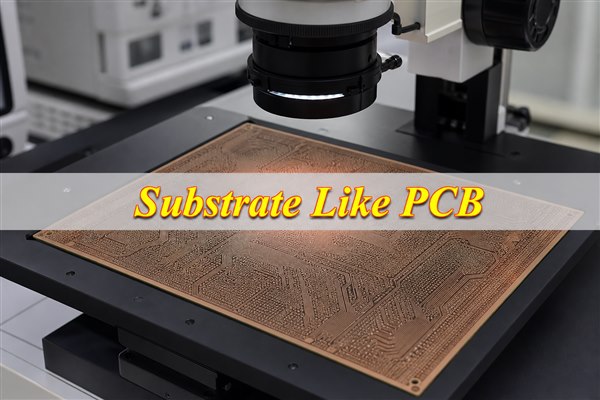
A substrate-like PCB (SLP) is an ultra-high-density circuit board positioned between an HDI PCB and an IC substrate. Consider it when component pitch, routing density, board area, or package integration exceeds practical conventional HDI capability. Because feasibility depends on the stackup, copper, dielectric, vias, panel format, inspection plan, and volume, confirm the complete construction through a design-for-manufacturing review.
EBest Circuit supports PCB design, prototyping, mass production, component sourcing, and assembly from China. For high-density projects, we review the full data package, separate confirmed requirements from items requiring process evaluation, and establish a realistic prototype-to-production plan. This produces a clearer quotation and reduces redesign, yield, and schedule risk.
What Is a Substrate-Like PCB?
A substrate-like PCB combines PCB-level assembly flexibility with interconnect features approaching those used in organic packaging substrates. It can carry conventional surface-mounted components while supporting finer routing, smaller microvias, and thinner buildup structures than many standard HDI boards. Substrate-like PCB technology describes a range of constructions, not one universal specification.
The word “substrate-like” does not mean the board is identical to a semiconductor package substrate. An IC substrate redistributes connections between a semiconductor die and the package terminals; the completed package then interfaces with the system board. An SLP remains a printed circuit board, but its fine-feature conductor formation, layer registration, materials, and inspection requirements may resemble packaging-substrate practices.
Classify the project by function before comparing minimum dimensions. A standard or HDI PCB provides board-level interconnection; an SLP supports board-level assembly at substantially higher routing density; an IC substrate connects the semiconductor die to its package and the system board. If the design requires package-level redistribution rather than board-level assembly, route it to an IC-substrate supplier.
How Does a Substrate-Like PCB Differ from an HDI PCB and IC Substrate?
The main differences are function, feature density, conductor-formation method, material system, and assembly interface. A high-density layout should not be called SLP only because it uses microvias. The classification must consider whether the complete structure requires substrate-level process control and whether the board still performs a PCB-level assembly role.
| Comparison Point | HDI PCB | Substrate-Like PCB | IC Substrate |
| System function | Connects packaged components at board level | Provides board-level interconnection for very dense packaged-component routing; any bare-die interface requires separate assembly and reliability qualification | Redistributes connections between the semiconductor die and the package terminals; the completed package then connects to the system board |
| Conductor formation | Subtractive processing is common; advanced designs may use finer processes | mSAP or related additive approaches are often considered when subtractive etching cannot hold the required geometry | Package-substrate processes are optimized for much finer redistribution features |
| Via structure | Laser blind vias, buried vias, and sequential buildup | Fine, tightly registered microvias with project-specific filling and sequential-buildup controls | Package-level microvias and redistribution structures |
| Materials | FR-4 and high-performance PCB laminates | Process-compatible thin buildup dielectrics and low-profile copper; the exact resin system is project-specific | BT, ABF, or other package-substrate material systems |
| Commercial risk | Typically the broadest supplier base and the lowest qualification burden of the three | Typically requires a narrower supplier search, process trials, and tighter yield controls | Requires a specialized package-substrate supply chain and package-level qualification |
Use HDI when it completes the routing with acceptable reliability and yield. Use SLP when HDI cannot meet board-level density. Use an IC substrate when the design requires package-level redistribution.
When Should You Choose a Substrate-Like PCB?
Choose SLP only when a measurable density or integration constraint cannot be solved efficiently with a conventional HDI structure. The trigger should come from package escape routing, board-area reduction, electrical performance, mixed component integration, or a defined system architecture—not from the desire to use a fashionable technology label.
- Routing density: Fine-pitch packages cannot escape through a practical HDI stackup without excessive layers or via congestion.
- Board area: The enclosure cannot accommodate the circuits, battery, sensors, connectors, and thermal features.
- Integration: Dense SMD placement must coexist with chip-on-board, flip-chip, or another controlled interface.
- Production case: Product value, forecast volume, and lifecycle justify the added process validation.
Stay with HDI when package selection, routing changes, or a modest layer increase solves the constraint with lower supply and yield risk.
Where Are Substrate-Like PCBs Commonly Used?
SLP technology is most useful where physical space, interconnect density, and system performance are tightly coupled. Smartphones and wearables are familiar examples, but the same selection logic can apply to computing, communications, medical, aerospace, and automotive electronics when the project can support the required qualification and supply chain.
- Mobile and wearable devices: Dense boards release space for batteries, sensors, cameras, and mechanical features.
- Computing and communications: Dense packages, short interconnects, and compact optical modules can require substrate-like routing.
- Medical and aerospace systems: Miniaturization may justify SLP only after environmental, traceability, and reliability requirements are qualified.
- Automotive electronics: Compact sensing and control modules require validated thermal cycling, materials, and production controls.
Choose the technology from the package map, stackup, environment, reliability plan, and quantity—not the industry label.
What Are the Substrate-Like PCB Design Requirements?
Substrate-like PCB design rules must be approved as one connected construction. Substrate-like PCB line width and spacing depend on copper thickness and conductor process; microvia size depends on dielectric thickness, pad geometry, filling, and stacking; impedance depends on the finished copper profile, dielectric properties, and reference-plane spacing.
- Line width and spacing: State the minimum by layer, finished copper thickness, and required process. Mark whether the value is isolated or repeated across dense routing areas, because a single demonstration trace does not establish production yield.
- Microvia construction: Define laser-drill diameter, dielectric depth, capture and target pads, copper filling, capping, and stacked or staggered structure. Review the complete via geometry against plating and thermal-cycling requirements.
- Layer registration: Set alignment tolerances for each buildup cycle and provide enough capture margin for material movement. Registration coupons should represent the critical layer pairs instead of measuring only the finished outline.
- Stackup and materials: Freeze layer order, dielectric type and thickness, copper profile, reference planes, and total thickness before routing sign-off. Material substitutions require renewed impedance, adhesion, and reliability review.
- Controlled impedance: Provide single-ended or differential targets, tolerance, routing layer, reference layer, trace geometry, and coupon requirements. The production stackup—not nominal CAD dimensions alone—must determine the final geometry.
- Copper and power integrity: Balance copper distribution, confirm plane continuity, and review current paths, return paths, and thermal spreading. Local fine routing must not weaken power delivery or create avoidable warpage.
- Assembly interface: Match pad definition, solder-mask openings, finish thickness, coplanarity, stencil strategy, and reflow profile to the package pitch. Confirm whether bare-die bonding or other special interfaces change cleanliness and finish requirements.
- Panel and inspection features: Define tooling, fiducials, coupons, rails, routing, panel support, and critical measurement locations before release. The panel must support both fabrication control and the intended assembly process.
EBest’s current general English PCB capability table does not establish a dedicated SLP or mSAP production window. Therefore, fine-feature limits must be quoted only after written confirmation of the stackup, copper thickness, dielectric system, conductor process, microvia structure, production site, order volume, and inspection plan.
Which Materials and Stackup Structures Are Used for Substrate-Like PCBs?
Material selection is driven by process compatibility, electrical performance, dimensional stability, adhesion, and reliability. There is no universal SLP laminate. Substrate-like PCB materials may include modified epoxy systems, BT-based materials, resin-coated copper, buildup films, or other organic dielectrics. The substrate-like PCB stackup must be selected together with the manufacturing route.
| Design Requirement | Material or Stackup Consideration | Main Risk | Evidence to Request |
| Fine conductor geometry | Low-profile copper and process-compatible dielectric surface | Weak adhesion, conductor variation, or residual copper | Approved material system and conductor inspection plan |
| Laser microvias | Controlled thin dielectric and laser-processable resin | Poor via formation, debris, voiding, or an unfavorable depth-to-diameter ratio | Via geometry limits, microsection criteria, and via-fill specification |
| High-speed signals | Controlled Dk/Df, copper profile, and dielectric thickness | Impedance drift and higher insertion loss | Material data, field-solver stackup, and impedance coupons |
| Thermal cycling | Compatible CTE, modulus, Tg, and stable resin-to-copper interfaces | Delamination, interfacial cracking, or via fatigue | Material data and an application-specific thermal-reliability plan |
| Thin total construction | Balanced buildup and copper distribution | Warpage and handling damage | Flatness plan, panel support, and assembly review |
Apply the finest geometry only where routing requires it. Review copper balance, buildup symmetry, resin flow, via sequence, reference planes, and assembly heat exposure together.
How Is a Substrate-Like PCB Manufactured?
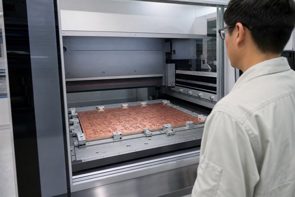
The substrate-like PCB manufacturing process combines tightly controlled imaging, conductor formation, buildup lamination, laser drilling, copper filling, registration, and inspection. The exact route varies by material and design. For very fine conductors, modified semi-additive processing can offer straighter conductor profiles than a purely subtractive route because copper is built within patterned resist and the thin seed layer is removed afterward.
- Manufacturing package review: Check Gerber or ODB++, stackup, copper, dielectrics, line/space by layer, microvias, impedance, finish, quantity, and reliability requirements. Close missing inputs before tooling.
- Process-route definition: Assign subtractive, semi-additive, or modified semi-additive processing by layer. Separate stable rules from features requiring coupons, trials, or design changes, and define the inspection gates before production.
- Material preparation: Verify material identity, thickness, copper profile, storage condition, and surface cleanliness. Prepare the surface for consistent adhesion, imaging, seed-layer deposition, and plating.
- Fine-conductor formation: Align the artwork and control resist thickness, exposure, and development. In an mSAP-type route, form the seed layer, pattern-plate the traces, strip the resist, and remove exposed seed copper without excessive side etching.
- Buildup lamination: Control temperature, pressure, vacuum, resin behavior, and dielectric thickness. Measure dimensional movement after lamination and apply approved compensation before the next imaging cycle.
- Laser microvia drilling: Match laser energy and focus to the dielectric and target copper. Inspect diameter, position, taper, bottom condition, and residue; clean the via before metallization to protect interface reliability.
- Via metallization and filling: Establish conductive coverage, then plate and fill under controlled chemistry, agitation, current density, and temperature. Inspect for voids, dimples, overplating, and weak bottom connections before planarization.
- Sequential buildup control: Repeat lamination, drilling, metallization, and conductor formation while tracking registration. Use coupons, dimensional measurements, AOI, and process data to prevent cumulative alignment error.
- Final finish and release: Apply solder mask and surface finish, then complete AOI, electrical test, dimensions, impedance, and microsections. Release the lot only after all acceptance criteria and traceability records pass.
Manufacturability depends on the complete route. Approve the stackup, materials, conductor process, microvia controls, inspection plan, and production conditions together rather than accepting a capability claim based on one machine or one minimum feature.
What Testing and Quality Control Are Required for Substrate-Like PCBs?
Quality control must verify both electrical continuity and the physical structures that create long-term reliability. A board can pass a basic open/short test while still containing weak microvias, marginal registration, conductor variation, or dielectric defects.
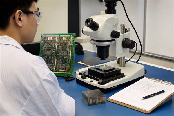
- AOI: Detect opens, shorts, residual copper, neck-down, and pattern deviations before buildup hides them.
- Electrical test: Verify continuity and isolation with coverage suited to net density and quantity.
- Microsections: Check copper, microvia shape and fill, interfaces, dielectric condition, and registration.
- Impedance and dimensions: Measure production coupons, board thickness, outline, feature position, and critical alignment.
- Reliability tests: Select thermal, moisture, and mechanical tests from the actual application conditions.
- Traceability: Link materials, process lots, inspections, deviations, and shipment records.
What Reliability and Manufacturing Risks Affect Substrate-Like PCBs?
The leading risks come from narrow process windows and interactions between materials, conductors, microvias, registration, and assembly heat. The earlier these risks are converted into measurable inspection and acceptance criteria, the easier it is to avoid disputes after fabrication.
| Risk | Likely Cause | Detection | Preventive Action |
| Residual copper or conductor variation | Imaging, plating, or flash-etch variation | AOI and dimensional coupon review | Control resist, seed layer, plating distribution, and etching window |
| Microvia voids or cracks | Drilling residue, poor metallization, filling defects, or thermal stress | Sample microsections plus performance-based thermal cycling with continuity monitoring | Control laser formation, desmear/cleaning, metallization, copper filling, and via-stack design |
| Layer misregistration | Material movement, lamination variation, or imaging alignment | Registration coupons and cross-sections; use X-ray only where the construction provides adequate contrast | Characterize material movement, apply approved compensation, and control buildup alignment |
| Delamination | Moisture, contamination, weak adhesion, or excessive thermal exposure | Visual inspection for external evidence, sample microsections, and thermal-stress or cycling tests | Control moisture storage, surface preparation, lamination, and the qualified assembly profile |
| Warpage | Unbalanced copper, asymmetric buildup, or material mismatch | Flatness measurement before and after thermal exposure | Balance stackup, copper distribution, panel support, and process conditions |
| Low or unstable production yield | Design rules based on isolated minimums instead of stable production windows | Prototype yield review and defect Pareto | Freeze production rules after DFM, trials, and acceptance review |
What Substrate-Like PCB Manufacturing Services Can We Provide?
EBest can review the design, plan prototypes, coordinate production, source components, and assemble boards, subject to approval of the submitted SLP construction.
- DFM review: Check escape routing, stackup, impedance, vias, panelization, and critical dimensions.
- Prototype plan: Separate buildable features from items requiring coupons, trials, or design changes.
- Volume preparation: Freeze materials, controls, acceptance criteria, documents, and change rules.
- Sourcing and assembly: Coordinate package availability, finish, stencil, placement, reflow, inspection, programming, and functional test.
Each quotation must confirm the production site, materials, fine-feature limits, volume, and test plan; company-wide capacity figures do not prove SLP capability.
Substrate-Like PCB Manufacturing Case Study
Project background: A representative compact control-module project combines fine-pitch packages, controlled-impedance interfaces, a fixed outline, and sequential buildup. The initial files apply one minimum line/space value across several layers but omit copper thickness, material grade, microvia filling, impedance tolerance, forecast volume, and reliability conditions.
Project requirements: The customer needs a buildable routing solution within the fixed outline, controlled impedance, measurable microvia and registration acceptance criteria, and a prototype route that can transfer to repeat production without reopening the complete design.
Our solution: EBest maps the critical escape regions, keeps wider and more stable geometry on noncritical layers, and reviews copper, dielectric, microvias, filling, impedance, and assembly heat as one construction. The DFM package defines registration coupons, microsection locations, impedance coupons, electrical-test coverage, traceability requirements, and quotation assumptions before tooling.
Output result: The customer receives a clear manufacturability package showing the proposed stackup, required design changes, trial items, material status, inspection criteria, quotation exclusions, and prototype-to-volume conditions. This allows the customer to choose an approved SLP route, a lower-risk HDI revision, a package change, or an IC-substrate solution before committing tooling cost and schedule.
Why Choose EBest for Substrate-Like PCB Manufacturing?
Choose EBest to obtain one accountable project path from design review through prototypes, sourcing, fabrication, assembly, and repeat production. The customer receives a written distinction between confirmed requirements, necessary design changes, trial items, and production-transfer conditions, reducing quotation gaps and late-stage surprises.
- Faster technical decisions: A structured DFM response separates buildable features from design changes, coupons, trials, and open questions before the customer approves tooling.
- Fewer supplier handoffs: PCB design, prototyping, mass production, component sourcing, and assembly can be coordinated through one commercial and technical workflow.
- Lower technology-selection risk: Experience across FR-4, multilayer, HDI, high-speed, impedance-controlled, flexible, rigid-flex, metal-core, ceramic, and IC-substrate products supports a practical comparison between SLP, HDI, and package-substrate routes.
- Controlled prototype-to-volume transfer: EBest defines material continuity, acceptance evidence, change control, and repeat-order conditions before the prototype is treated as a production baseline.
- Documented quality support: EBest reports ISO 9001:2015, ISO 13485:2016, IATF 16949, AS9100D, and UL credentials, together with RoHS and REACH compliance. Customers can request the applicable certificate scope and compliance documents for supplier approval.
- Capacity and schedule visibility: EBest reports company-wide capacity of 260,000 square feet and more than 1,000 different board part numbers per month. Material availability, process trials, inspection coverage, and the approved SLP construction are checked before an expedited schedule is committed.
What Factors Affect Substrate-Like PCB Cost and Lead Time?
Substrate-like PCB cost and lead time rise when the design reduces process margin, requires uncommon materials, adds buildup cycles, or demands extensive qualification. A credible quotation should show the assumptions behind the price and schedule rather than treating “SLP” as one fixed product category.
- Fine-feature density: Repeated narrow lines affect imaging, plating, inspection, and yield.
- Buildup cycles: More lamination and microvia cycles add time and registration risk.
- Materials: Buildup films, BT systems, low-loss laminates, and low-profile copper may extend sourcing time.
- Microvias: Filled, stacked, staggered, or multiple-depth structures add drilling, plating, planarization, and inspection steps.
- Panel and tests: Coupons, tooling margins, low utilization, impedance, microsections, and reliability tests increase cost.
- Production maturity: First builds require more engineering and risk allowance than frozen repeat orders.
Confirm material, tooling, trials, and inspection before accepting an expedited schedule.
What Information Is Required for a Substrate-Like PCB Quote?
A complete RFQ must define both the physical board and the evidence needed to accept it. Sending only Gerber files and a quantity often leaves the supplier to guess the stackup, material, microvia structure, impedance, finish, inspection, and production assumptions.
- Fabrication data: Gerber or ODB++, NC drill, IPC-356 netlist where available, and fabrication drawing.
- Stackup and materials: Layer order, copper, dielectrics, total thickness, buildup sequence, material grades, equivalents, and restrictions.
- Critical features: Line/space by layer, package pitch, critical pads, and isolated versus repeated minimums.
- Vias: Type, diameter, depth, stacking or staggering, filling, capping, and acceptance criteria.
- Electrical and surface: Impedance, tolerance, coupon plan, finish, solder-mask definition, and assembly interface.
- Quality and commercial: Inspection, microsections, reports, traceability, reliability tests, quantity, annual volume, destination, and target date.
- Assembly package: BOM, centroid file, drawings, stencil, programming, and functional-test requirements.
Send the package with a list of critical-to-quality characteristics. The engineering response should separate confirmed capability, proposed DFM changes, material availability, open questions, quotation assumptions, and items requiring evaluation.
FAQs About Substrate-Like PCBs
Q1: Can an SLP prototype use different materials or processes from mass production?
A1: Yes, but document every material and process difference and its effect on dielectric properties, copper profile, microvia reliability, impedance, and assembly. A prototype built through a different route is not proof of volume readiness.
Q2: When is a pilot lot required before mass production?
A2: Use a pilot lot when any critical construction or production condition is new, including the stackup, material, fine-feature rule, microvia structure, factory route, panel format, or acceptance plan. Set the sample size and pass criteria before production starts.
Q3: What should happen if a microsection fails but the electrical test passes?
A3: Hold the affected lot and investigate the structural defect. Electrical continuity at room temperature does not prove acceptable copper interfaces, via filling, or thermal-cycle reliability.
Q4: Can fine-line SLP conductors or microvias be repaired?
A4: Do not assume fine-line conductor or microvia repair is acceptable. Repair can change geometry, impedance, adhesion, and reliability. Define prohibited defects, permitted repair methods, inspection evidence, and customer approval requirements before production.
Q5: Does an SLP require special storage or handling before assembly?
A5: Requirements depend on the dielectric, finish, thickness, moisture sensitivity, and assembly profile. Define packaging, humidity control, bake conditions, shelf life, and handling limits in the purchase and assembly specifications.
If you are sourcing a substrate-like PCB manufacturer in China, send your Gerber/ODB++, stackup, material requirements, copper thickness, target line/space, via structure, impedance table, quantity, assembly data, and test requirements to sales@bestpcbs.com. EBest will review the design, identify confirmed capabilities and open risks, and prepare a quotation based on the actual manufacturing package.







