EBest Circuit (Best Technology) is your trusted partner for comprehensive PCB solutions — from initial concept to final product. With over 18 years of experience, we offer one-stop services that cover the full PCB lifecycle, ensuring high quality, fast turnaround, and competitive pricing. Why customers prefer us:
- Free DFM/DFA check
- Free Design Guideline
- 25,000m2 production capacity
- 2 Hours quick response
- Quote within 12 hours
- Online support 24/7
- Transparent order tracking from first day to final delivery
- Military-grade quality boards with strict testing and IPC standards
- One-stop services from layout to turnkey assembly
- Engineering support to optimize your design for performance and cost
- Global delivery and localized service teams
- Reliable fabrication with IPC Class 2/3 standards
- ISO13485, ISO9001, AS9100D, IATF16949 certificated
Whether you’re a startup building your first prototype or a large OEM scaling up production, EBest Circuit (Best Technology) is your reliable PCB partner.
Our Core Services – From Design to Assembly
We provide a wide range of services to support your project at every stage:
- PCB Design & DFM Check – We don’t just manufacture—we help you build better boards. Send us your layout or concept, and our senior engineers will review your files for manufacturability, improving your design before it hits the production line.
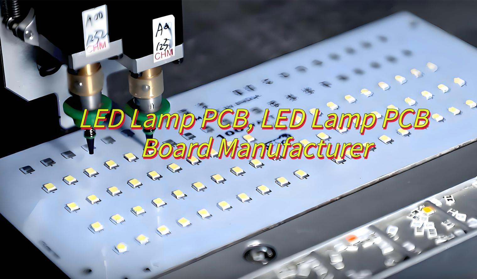
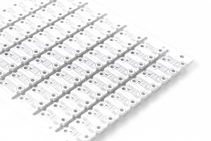
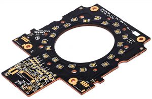
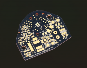
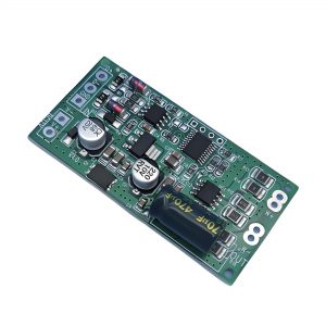
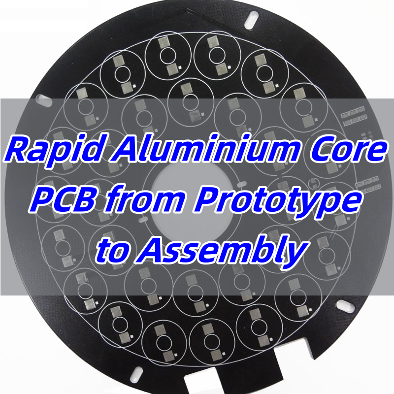
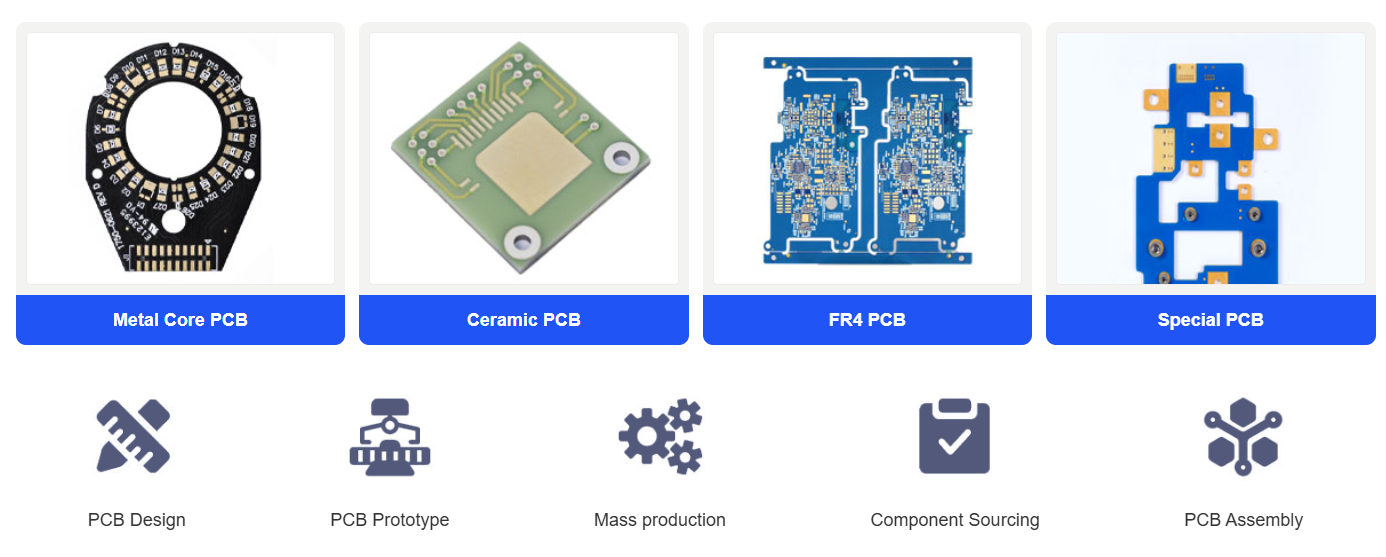
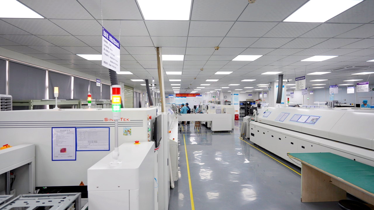
- PCB Fabrication – Single-layer, multi-layer, HDI, aluminum-based, or ceramic—we fabricate PCBs of all complexities. Our in-house plant supports quick turnarounds and strict quality control for every batch.
- PCB Prototype – Need your prototype in 24–72 hours? We’ve got your back. Ideal for engineers in the development phase, we offer fast PCB prototyping with full traceability, fly-probe testing, and surface finish options.
- PCB Assembly – Our turnkey PCB assembly service covers everything from component sourcing, SMT/DIP soldering, to functional testing. You send us your BOM and Gerber—we handle the rest.
- Components Sourcing – Reliable sourcing of original, competitive prices, traceable electronic components.
- IC Programming – Pre-programming and testing of integrated circuits to streamline your assembly process.
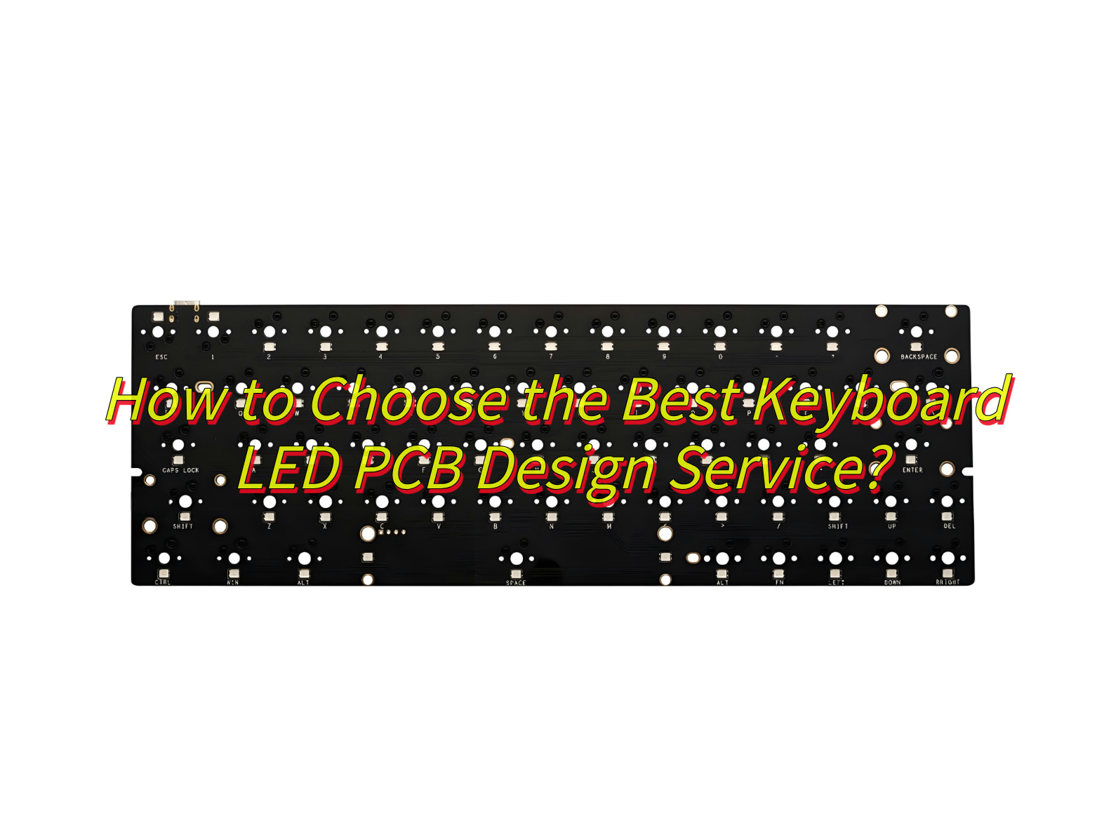
What PCB Types Does EBest Circuit (Best Technology) Manufactured?
We are capable of manufacturing a wide variety of PCB types, including but not limited to:
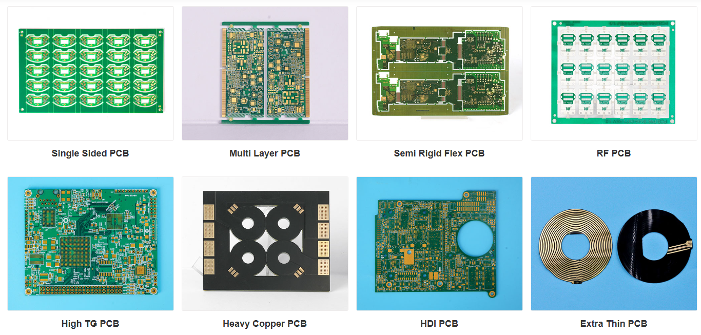
- FR4 PCBs (high speed PCB, IC substrate, high TG PCB, extra thin PCB, our special semi-rigid flex PCB and so on.)
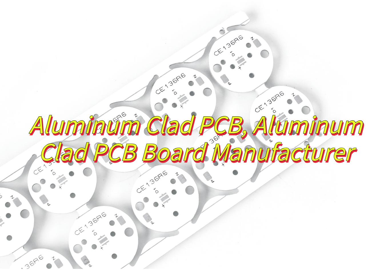
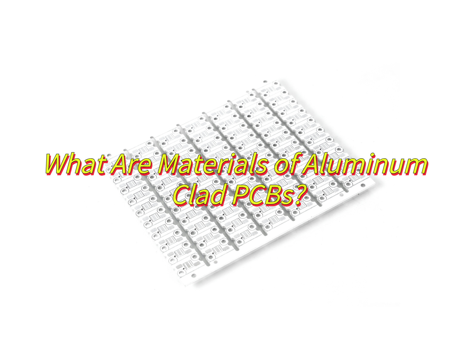
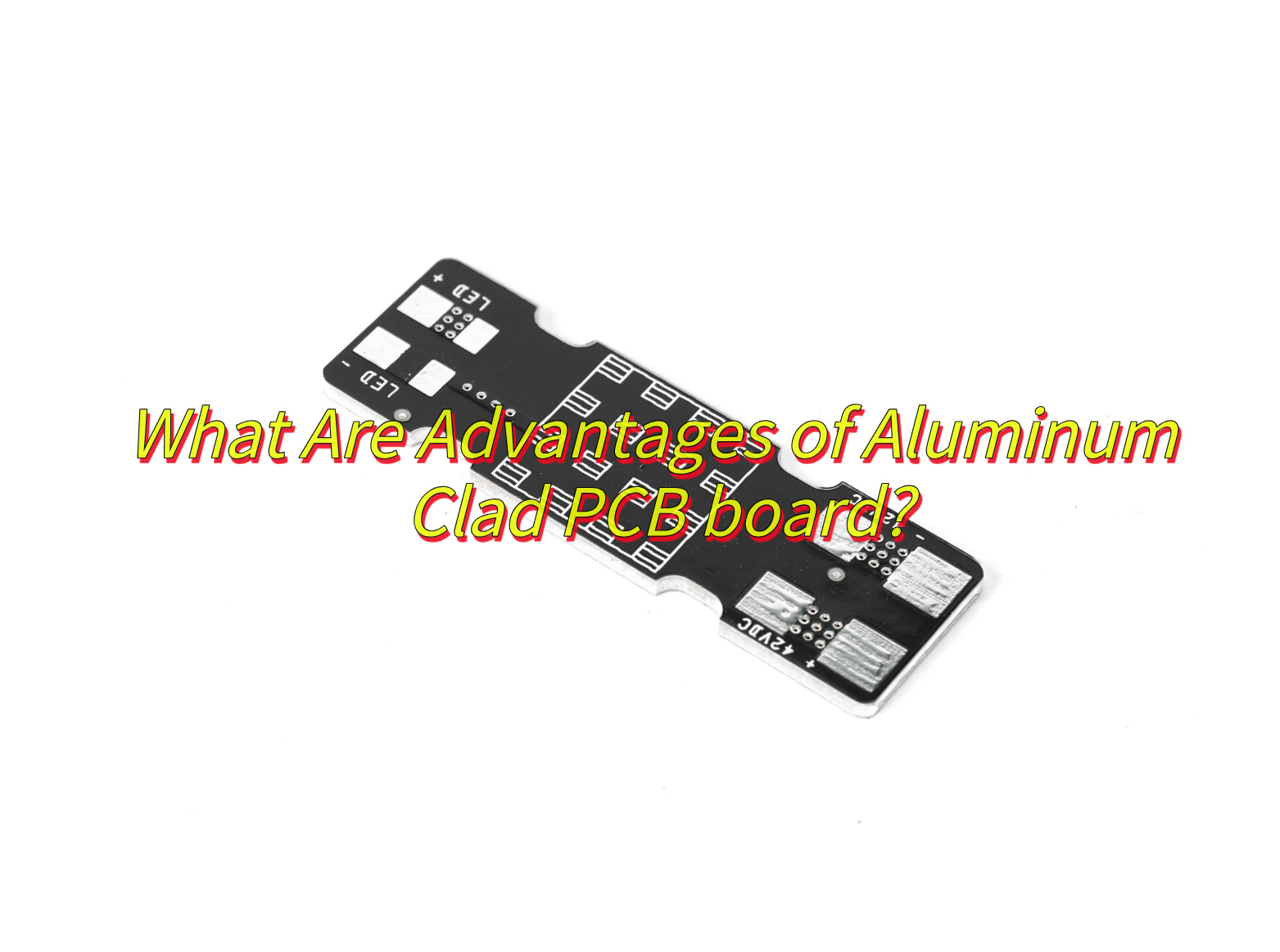
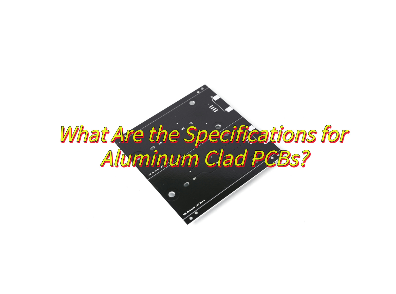
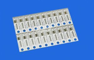
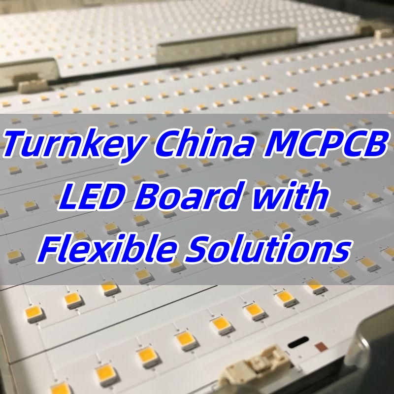
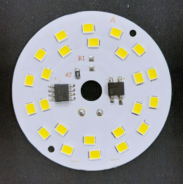
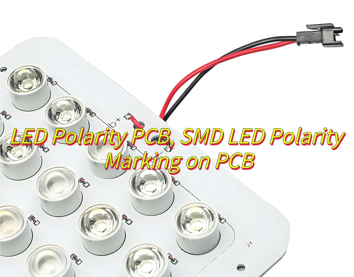
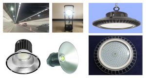
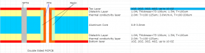
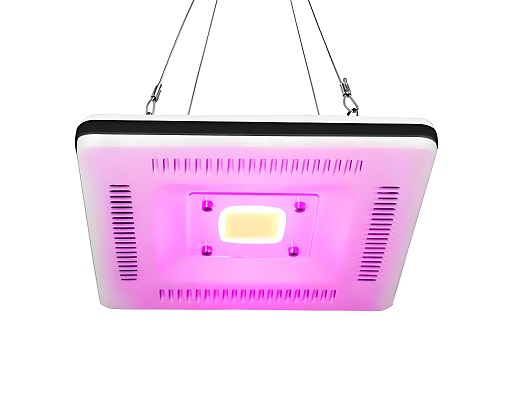
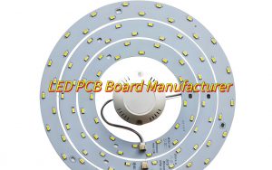
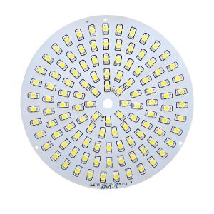
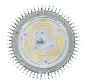
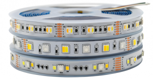
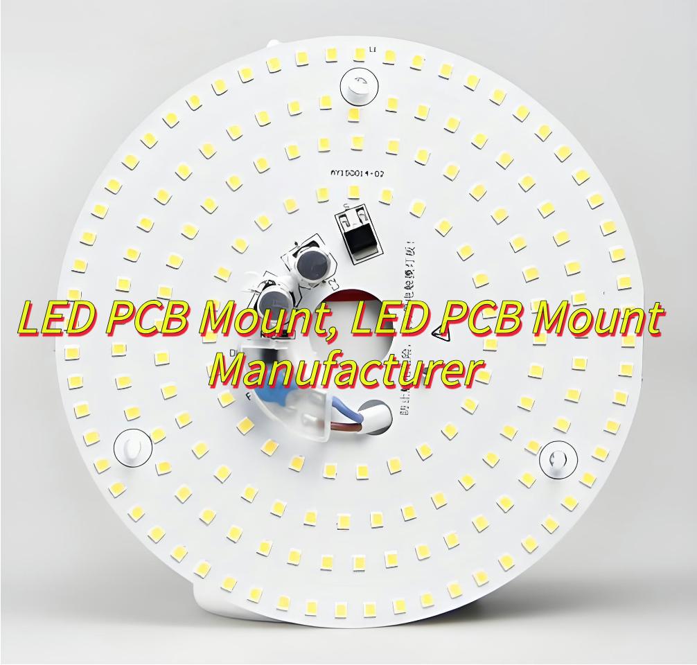
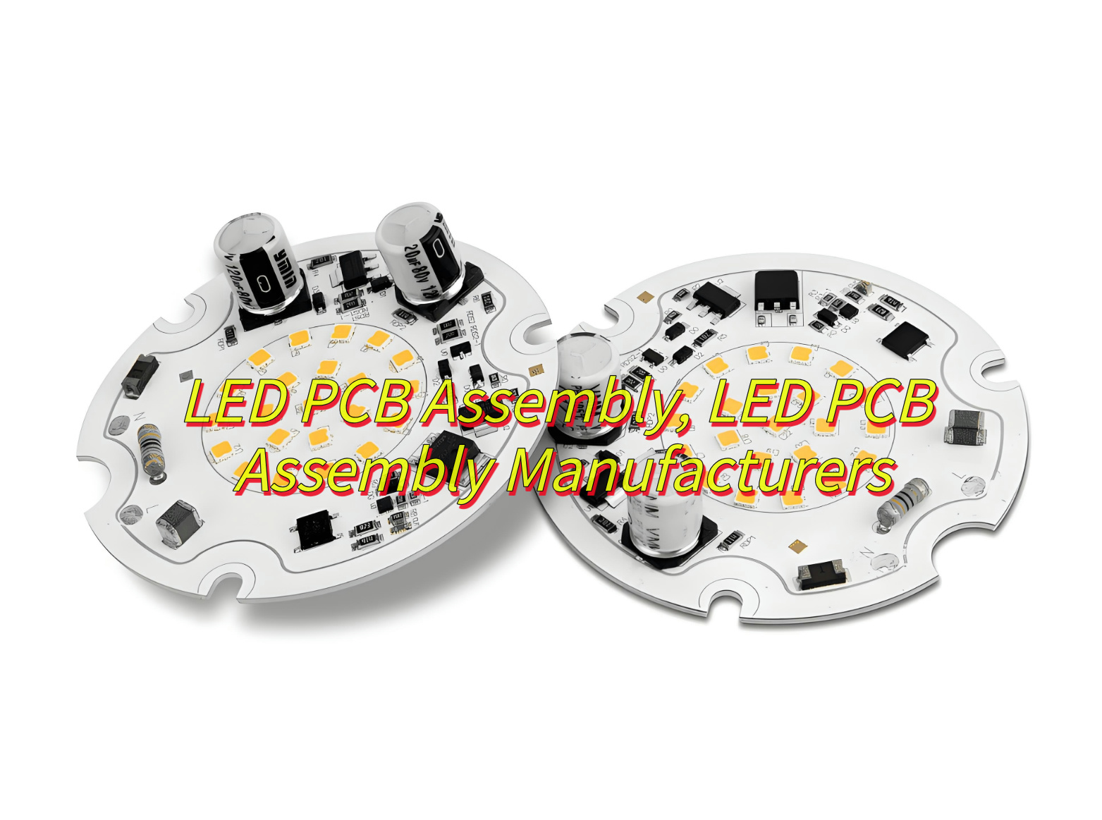
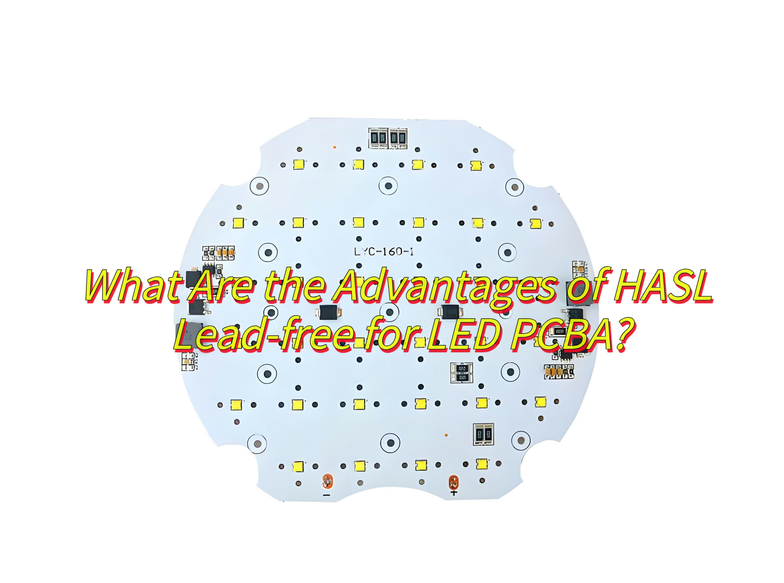
- Metal Core MCPCBs (aluminum based PCB, copper clad PCB, sinkpad PCB, thermoelectric copper separate PCB)
- Ceramic PCBs (AlN, BeO, Al₂O₃, Zro2)
- Flexible and Rigid-Flex PCBs, FFC, Dual access PCB
- HDI PCBs
- High-Frequency PCBs
- Heavy Copper PCBs
- Busbar PCBs
- Hybrid Substrate PCBs
Whether you need high-reliability boards for aerospace, thermally conductive boards for LEDs, or RF boards for communication devices, we have the capability to deliver.
PCB Prototype Lead Time
We understand how crucial speed is in product development. Our standard PCB prototype lead time is:
- Single-layer & double-layer PCBs: as fast as 24 hours
- 4-layer PCBs: typically 48–72 hours
- 6-layer or above: around 3–5 working days, depending on complexity
Below is a detailed prototype lead time sheet at EBest Circuit (Best Technology), the expedited options are available to meet urgent project deadlines.
| Prototype(<1m²) | Layers | Normal Service | Expedited Service |
| FR4 PCB | 1 Layer | 3-4 days | 24 hours |
| 2 Layers | 4-6 days | 24 hours | |
| 4 Layers | 8-10 days | 48 hours | |
| 6 Layers | 8-10 days | 72 hours | |
| 8 Layers | 10~14 days | 72-96 hours | |
| 10 Layers | 14-18 days | 72-96 hours | |
| HDI (1+N+1 2+N+2) | 2.5 – 3.5weeks | TBD (depend on design) |
EBest Circuit (Best Technology)’s PCB Assembly Capabilities
And as a one-stop service provider to customers, we offer PCB assembly service as well, such as:
- SMT (Surface-Mount Technology)
- DIP (Dual In-line Package)
- Reflow Soldering (for SMD components)
- Wave Soldering (for DIP components)
- Hand Soldering (connectors, through hole components)
- Mixed Assembly Technologies
- Wire Harness Assembly
- PCBA Testing
- Box Building Assembly
How to Work with us – From File to Finished Board?
Step 1: Upload Your Files
Submit your Gerber, BOM, or PCB design files via our secure portal. We support various formats and guarantee file confidentiality.
Step 2: Engineering Review & Instant Quote
Our team performs a DFM check and confirms design compatibility. You’ll receive a quote and estimated lead time within 2 hours.
Step 3: PCB Fabrication & Parts Procurement
We begin board production and source parts simultaneously through authorized channels like Mouser, DigiKey, and Arrow.
Step 4: SMT/DIP Assembly & Testing
Boards are assembled in our SMT lines with 3D AOI, X-ray, and functional testing to ensure performance and soldering quality.
Step 5: Secure Packaging & Global Shipping
We pack your PCBs using anti-static materials and ship via DHL, FedEx, or your chosen method. Worldwide delivery in 3–5 days.
Custom PCB Board Quote
Not sure about all your PCB specs? No problem — we’re here to help.
Request a custom PCB board quotation if your project includes any of the following advanced requirements:
- Controlled Impedance
- Via Filling or Plugging
- Blind or Buried Vias
- Heavy Copper (≥ 2oz)
- Controlled Dielectric Thickness
- Edge Plating
- CPK Requirements
Simply share what you do know — our engineering team will review your files and guide you through the rest.
FAQs
Q1: What file formats do you support?
Gerber (RS-274X), BOM (Excel), Centroid files, Pick & Place, Altium, Eagle, and PDF for reference.
Q2: Can I order just a few prototype boards?
Yes, our minimum order starts from 1 piece for PCB prototypes.
Q3: Do you provide components?
Yes! We offer full turnkey assembly, including sourcing components from trusted suppliers.
Q4: How do you ensure quality?
Every board is electrically tested (flying probe/fixture), and assembly passes AOI and functional testing before shipment.
Q5: Do you offer NDA for file protection?
Absolutely. We provide NDA upon request and all files are kept confidential.