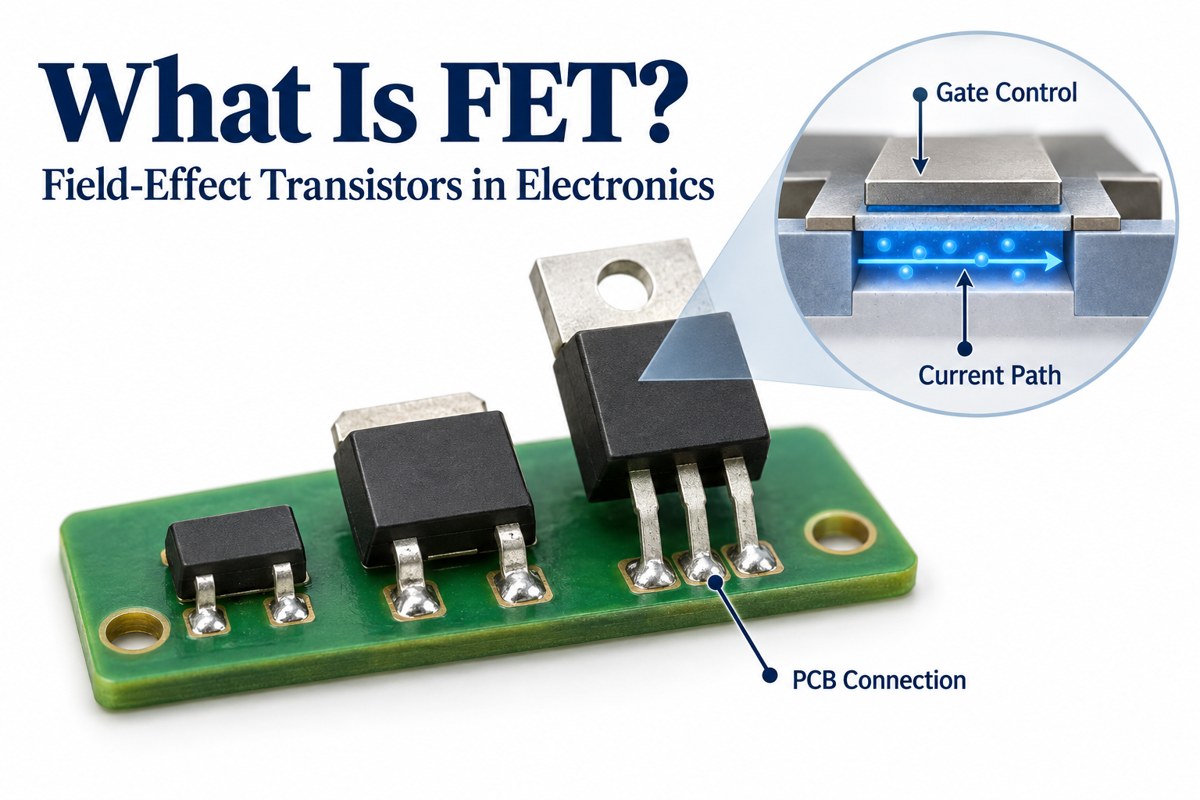
FET stands for field-effect transistor, a semiconductor device that uses an electric field to control current between its source and drain terminals. The gate voltage controls this current, allowing a FET to act as a switch or amplifier. JFETs and MOSFETs are two common families; MOSFETs are widely used in power supplies, motor drivers and digital circuits. For a PCB design, selecting a FET means matching its voltage rating, gate-drive requirements, losses and package to the circuit—not simply choosing a part with a high current rating.
Key Takeaways
- A FET controls source-to-drain conduction through its gate electric field; its three main terminals are gate, source and drain.
- A MOSFET is a type of FET, not a separate category alongside FETs.
- Conventional JFETs are normally on at zero gate-to-source voltage. Enhancement-mode MOSFETs are normally off; depletion-mode MOSFETs are normally on.
- N-channel and P-channel devices require different gate-voltage polarities, measured relative to the source.
- Threshold voltage does not guarantee low on-resistance. Check the specified RDS(on) at the available gate-drive voltage.
- FETs serve switching, amplification and power-management functions. Gate charge, safe operating area and cooling matter alongside voltage and current ratings.
- PCB performance depends on the correct footprint, gate-loop layout, thermal path, solder joints and electrical verification—not the transistor datasheet alone.
What Is FET in Electronics?
A FET is a voltage-controlled transistor whose gate field changes the conductivity of a semiconductor channel. It can regulate an analog signal or switch a load, depending on the device and circuit bias.
- Gate (G): the control terminal.
- Source (S): the reference terminal for gate-control voltage.
- Drain (D): the other terminal of the controlled current path.
The important control voltage is VGS, or gate voltage minus source voltage. A gate at 5 V does not necessarily mean VGS is 5 V: if the source is at 4 V, VGS is only 1 V. Many discrete MOSFETs have their body connected internally to the source, while integrated devices may expose or control the body differently.
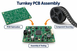
At EBest Circuit, we support the board surrounding these devices through PCB fabrication, component sourcing and PCB assembly services. The component part number, package drawing and circuit test requirements give our team the information needed to review the assembly.
FET Types: How Do JFETs and MOSFETs Differ?
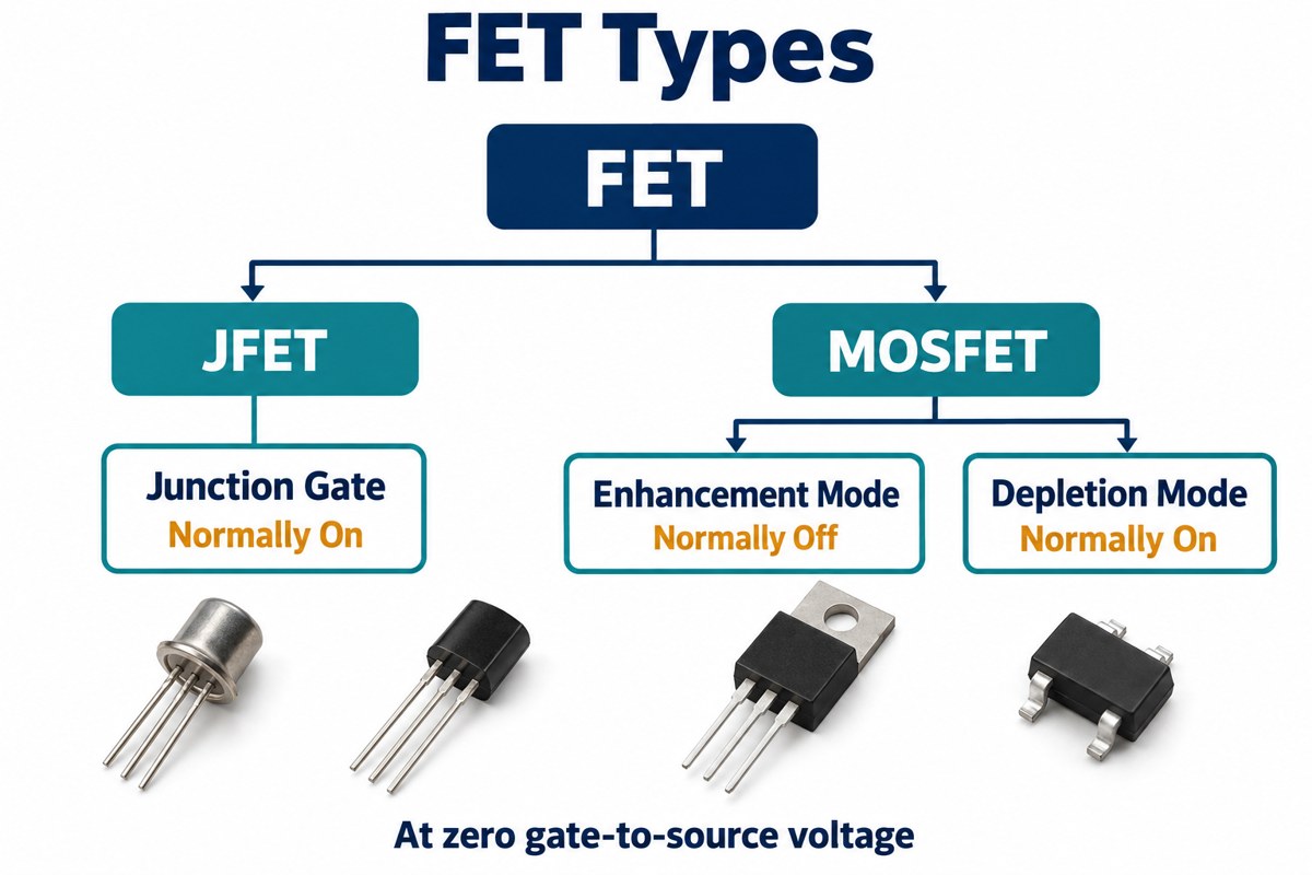
JFETs control a conducting channel with a reverse-biased junction gate; MOSFETs use an insulated gate. This difference changes their input behavior, bias requirements and common applications.
| Type | Gate structure | State at VGS = 0 | Typical use |
| JFET | PN junction | Normally on | High-input-impedance buffers, analog front ends, current sources |
| Enhancement-mode MOSFET | Insulated gate | Normally off | Load switches, converters, motor drivers, logic |
| Depletion-mode MOSFET | Insulated gate | Normally on | Bias circuits, startup circuits, current regulation |
These are common FET types, not an exhaustive list of every field-effect device. N-channel and P-channel describe channel polarity; enhancement and depletion describe behavior at zero gate-to-source voltage. They are different classification axes, not interchangeable names.
How Does a FET Work?
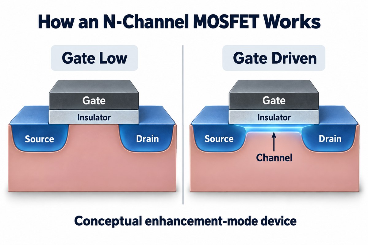
A FET works by changing its channel conductivity in response to gate-to-source voltage. The gate controls the channel; it does not supply the load current.
For an enhancement-mode N-channel MOSFET, the FET working principle can be followed in three stages:
- Gate held at the source potential: the intended channel is off, although leakage and body-diode conduction still need consideration.
- Positive VGS applied: an electric field establishes a conducting channel. Near threshold, only the specified small test current is assured.
- Adequate gate drive applied: the channel can reach low resistance under the datasheet conditions, allowing efficient switching within the device limits.
A conventional N-channel JFET behaves differently: its channel conducts at VGS = 0, and a negative gate-to-source bias narrows the channel until it approaches cutoff. Amplifier circuits bias either device in a suitable operating region rather than simply switching between on and off.
What Is MOSFET, and Why Is Gate Drive Important?
MOSFET means metal-oxide-semiconductor field-effect transistor. Its insulated gate draws little steady-state current, but a driver must charge and discharge the gate capacitances when switching.
This is why a microcontroller pin may switch a small signal MOSFET slowly yet be unsuitable for a larger device at high frequency. Total gate charge, switching frequency and the required transition time determine the driver demand. Gate leakage is not the same as switching-drive current.
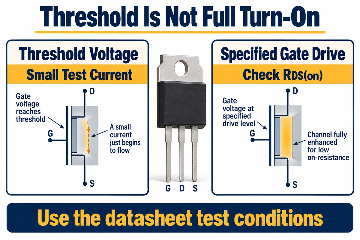
VGS(th) is not a recommended full-load drive voltage. For example, onsemi’s 2N7002E datasheet specifies a 1.0–2.5 V threshold range at just 250 µA. Its maximum on-resistance is specified separately: 3.0 Ω at VGS = 4.5 V and ID = 50 mA, or 2.5 Ω at VGS = 10 V and ID = 240 mA, at 25°C under the stated pulse-test conditions.
Those values do not establish a guaranteed maximum RDS(on) at 3.3 V. For a 3.3 V control output, choose a device with an appropriate guaranteed resistance specification at that drive level or lower, or provide a suitable gate driver. Also keep VGS within its absolute maximum rating during ringing and transients.
How Do N-Channel and P-Channel FETs Differ?
N-channel devices use electrons as their majority carriers, while P-channel devices use holes. For enhancement-mode MOSFET switching, an N-channel device needs positive VGS; a P-channel device needs negative VGS.
- N-channel low-side switch: commonly placed between the load and ground. A ground-referenced source makes gate drive straightforward.
- N-channel high-side switch: usually needs a driver that raises the gate above the moving source potential.
- P-channel high-side switch: can turn on by pulling its gate below the source, provided the circuit limits VGS correctly.
The polarity rule alone does not apply unchanged to every JFET or depletion-mode circuit. Check the exact device type before interpreting gate voltages. Package shape also does not identify channel polarity or pin order.
What Is the Difference Between a FET and a BJT?
A FET controls conduction through a gate electric field; a bipolar junction transistor uses base-emitter bias and carrier injection, normally requiring continuous base-drive current. Both can switch or amplify signals.
| Feature | FET | BJT |
| Main terminals | Gate, source, drain | Base, emitter, collector |
| Control interface | Gate-to-source voltage | Base-emitter bias with base current |
| Input loading | Typically high input impedance | Depends on base current and bias network |
| Switching-drive concern | Gate charge and voltage | Base-drive current and stored charge |
A MOSFET is often attractive for efficient power switching, but a BJT may suit a low-cost signal stage or particular analog requirement. Neither device is universally quieter, faster or cooler; compare the actual parts and their operating conditions.
Where Are FETs Used on PCBs?
FETs are used on PCBs to switch power, amplify signals and control current in converters, drivers and input circuits.
- DC-DC converters: MOSFETs switch energy into inductors and can provide synchronous rectification.
- Motor and LED drivers: power MOSFETs control load current, often with pulse-width modulation.
- Load switches and battery circuits: devices connect or disconnect power paths; reverse blocking may require paired MOSFETs.
- Analog inputs: JFETs and FET-input amplifiers reduce loading on high-impedance signal sources.
- Level shifting: selected small-signal MOSFET circuits translate logic levels when their topology and speed suit the interface.
The onsemi 2N7002E is a 60 V N-channel MOSFET in SOT-23, with low-side switching and level shifting among its listed applications. It is a small-signal example, not a substitute for a power MOSFET sized for a multiamp motor load.
Which FET Parameters Matter for Selection?
For a switching MOSFET, start with voltage stress, available gate drive, operating current, switching losses and thermal conditions. Then verify that the package and safe operating area support the intended duty.
| Parameter | Selection check |
| VDS rating | Account for supply voltage and measured or predicted overshoot. |
| RDS(on) | Use the guaranteed value at the available VGS and allow for temperature rise. |
| Gate charge, Qg | Match the driver to switching frequency and transition-time requirements. |
| Safe operating area | Check startup, inrush and linear-mode stress, not only steady current. |
| Thermal data | Use conditions relevant to the actual PCB, copper, airflow and heatsink. |
| Package and pinout | Match the exact manufacturer land pattern and terminal assignment. |
For a simple conduction-loss estimate, P = I² × RDS(on). An illustrative 2 A current through 50 mΩ produces 0.20 W while conducting continuously. This excludes switching and other losses; the resistance must reflect operating temperature. A large current number on a datasheet front page is not a guarantee for a small copper pad on your board.
What PCB Layout and Assembly Checks Matter for FETs?
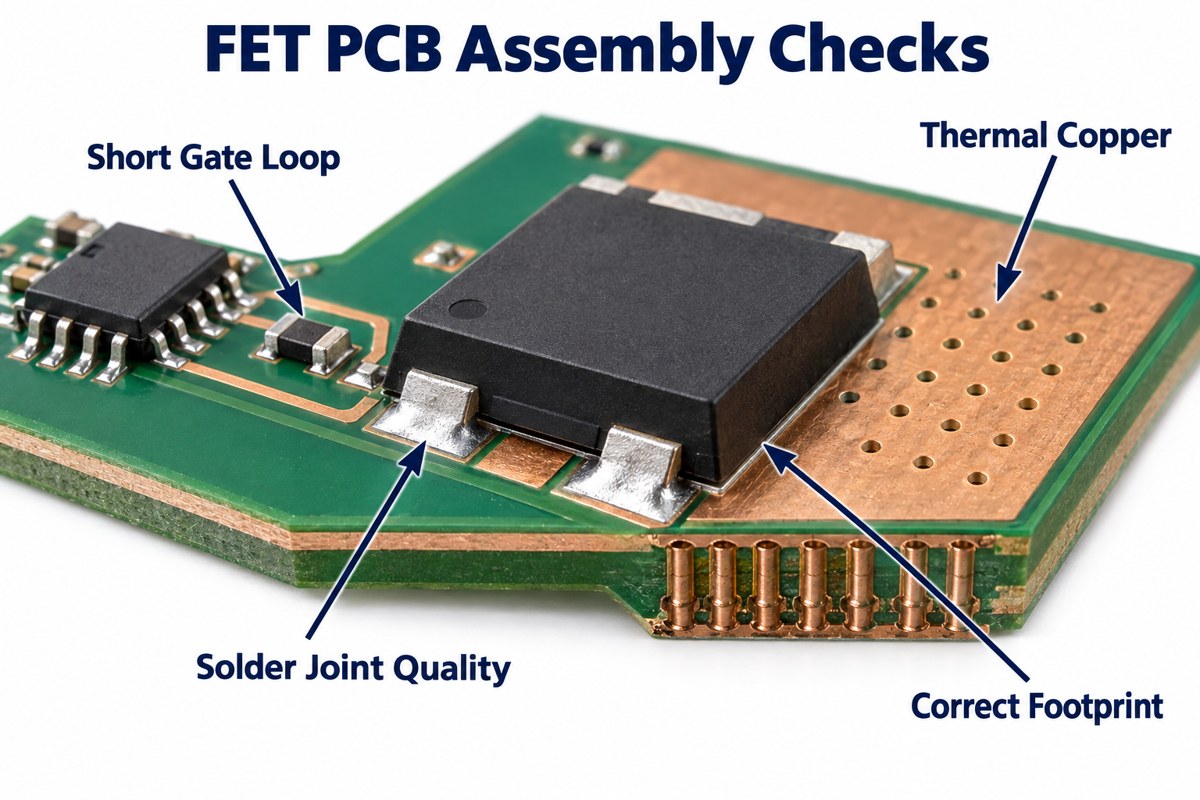
The most important board-level checks are the correct pinout, a compact gate-drive loop, a viable heat path and verified solder connections. Each addresses a different failure mechanism.
- Footprint and orientation: match the approved ordering code and package drawing. Similar SOT-23 or power packages can have different assignments.
- Gate loop: keep the driver, gate resistor and source-return path compact. Avoid sharing a sensitive gate return with a high-current path when the device provides a separate source-sense connection.
- Thermal connection: follow the package guidance for exposed pads, copper spreading and thermal vias. Do not connect a drain pad to ground simply because it is a thermal pad.
- Solder deposition: review stencil openings and paste volume for the actual package. Excess paste, insufficient wetting or hidden-pad voiding may impair assembly quality.
- Verification: combine appropriate visual/AOI or X-ray inspection with electrical testing. Measure gate drive and temperature under the specified load; a good-looking joint does not prove correct switching.
Before production, a PCB prototype build can help validate footprint fit, accessible test points and assembly behavior. The illustrations here explain concepts; they are not fabrication drawings or universal package pinouts.
FAQ About FETs
Can a FET conduct current in both directions?
An enhanced MOSFET channel can conduct in either direction, but a conventional discrete power MOSFET also has a body diode. Consequently, turning the gate off does not provide blocking in both directions. Bidirectional isolation often uses back-to-back MOSFETs with a suitable control circuit. Verify the topology rather than treating one transistor as an ideal relay.
Does “FET” always mean MOSFET on a schematic?
No. FET is the broader device family. Informal power-electronics discussions often shorten MOSFET to FET, but a schematic may use a JFET or another field-effect device. The part number, symbol and datasheet—not the abbreviation alone—identify its technology, polarity, operating mode and terminal connections.
Why can a FET turn on when its gate is disconnected?
An insulated MOSFET gate can retain charge or pick up coupled noise when left floating. A gate-to-source pull resistor can establish a defined state, with its value chosen for leakage, noise immunity and driver loading. Keep unpowered devices under proper ESD handling; a floating gate is not a reliable off command.
Can a multimeter confirm that a MOSFET is good?
A multimeter can reveal some shorts or a body-diode path, but it cannot prove rated-voltage blocking, correct gate charge, full-load resistance or switching performance. In-circuit parallel paths can also mislead readings. Disconnect power and discharge stored energy before basic checks; use an appropriate controlled test setup for functional verification.
Can one FET replace another with the same voltage rating?
Not automatically. The replacement must also match channel type, operating mode, footprint, pinout and gate-drive requirements. Compare on-resistance, gate charge, safe operating area and thermal behavior. Changes in switching speed or capacitance may affect ringing and EMI even when the new part has a higher nominal current rating.
Need Support Building a FET-Based PCB?
At EBest Circuit, we have supported PCB and PCBA projects since 2006. We can coordinate bare-board fabrication, component sourcing and assembly for your approved FET-based design, with inspection and test requirements agreed for the project.
Send your Gerber files, BOM with exact FET part numbers, assembly drawings, quantity and test requirements to sales@bestpcbs.com. Include the load current, gate-drive voltage and any thermal requirements so we can review the board and assembly needs before quoting.